
|
|
| Elliott Sound Products | Audio Designs With Opamps - 3 |
Copyright © 2006 - Rod Elliott (ESP)
 Main Index
Articles Index
Main Index
Articles Index
Probably the best known common mode circuit is the single opamp balanced receiver circuit. While it has a number of perceived problems in real life, it is nonetheless a good place to start. The problems with the circuit are normally not a limitation. The schematic is shown below, and there are two circuits shown. The first shows the circuit the way it is normally used, with the input (source) connected in differential mode to the opamp inputs. The second circuit shows how the circuit connects to the input for noise input - it is coupled (ideally) equally to both inputs at once.
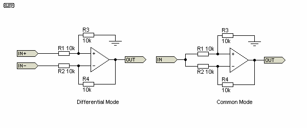
Figure 22 - Differential Input Opamp Circuit
While the wanted signal is passed directly through to the output (but is now a simple ground referenced signal at that point), any noise is presented to both inputs at equal level. This causes the cancellation of the noise, while allowing the signal to pass without alteration. This is shown in Figure 23, where we have a microphone with 10mV (differential) output, in the presence of a 100Hz 1V common mode noise signal. This is a ratio of 1:100 of signal to noise (or 100:1 noise to signal).
Although the results I obtained are simulated, the reality is not much different. At the output, the interference signal was measured at 27µV, while the signal level remains at 10mV. This means that the wanted signal is 51dB greater than the interference after the opamp, where the external noise level is 40dB greater than the signal at the input. The common mode rejection is therefore 91dB (1V common mode input, 27µV noise output). This is under ideal conditions, but in practice it is usually possible to get performance that exceeds the ability of the cable to maintain a perfect balance.
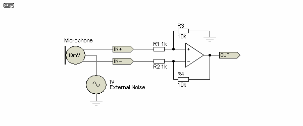
Figure 23 - Microphone Input Amplifier Circuit
Although there are a number of claimed problems with this circuit, in reality it works very well. There are better alternatives (especially for microphones), and these are well represented on the ESP site. The general principle of all balanced circuits remains the same as that shown above.
The biggest limitation of the Figure 23 circuit is that the input impedance for common mode (noise) signals is only equal if the signal applied to each input is equal. This is often claimed to cause major deficiencies in use, but in reality the common mode noise signal usually is very close to equal levels at each input, so the circuit works as described. The greatest limitation of this circuit for microphone use is opamp noise and reduced performance for high frequency common mode signals. For example, at 10kHz, the common mode rejection ratio is 6dB worse than at 100Hz.
Resistor tolerances, cable asymmetry and internal wiring will generally cause more error than the circuit limitations will impose. For optimum CMRR, the resistors should be 0.1% tolerance, and these may be selected from a batch of 1% components.
Although these are discussed in depth elsewhere on the ESP site, a brief look at these essential circuits is worthwhile here. Since we have balanced input circuits, it makes sense to have a matching output circuit, allowing equipment to provide a balanced output to other (often remote) gear. The basic circuit shown below is the starting point, and is the basis of all other (often much more complex) circuits.
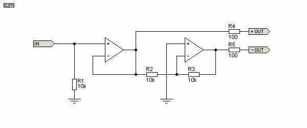
Figure 24 - Balanced Line Driver Circuit
The general idea is quite simple. A single-ended (unbalanced) signal is applied to the input, and it is buffered by the first opamp, and inverted by the second. You should recognise the inverting buffer from Part 1 of this series. The tolerance of the resistors around the inverting stage is again critical, and they should be as closely matched as possible to ensure that the two output signals are exactly the same, but with the signal from the second opamp inverted.
This is a true balanced output, but it has an inferred reference to ground. It behaves like a transformer with a grounded centre tap. While it is possible to approximate a fully floating output, in general it is not necessary to do so. It is usually essential to place a small resistance (typically around 100 ohms) in series with each output to prevent oscillation - R4 and R5. The cable connected to the opamp output acts as an unterminated transmission line at high frequencies, and this can cause the opamps to become unstable because of the reactive load. By including a resistance, the opamp's output is isolated from the reactive load and stability is usually unaffected, regardless of load.
While there is a small error caused by operating two opamps in series (therefore adding the propagation delay of each opamp), the circuit still maintains extremely good balance well above the audio band. Operating the inverting and non-inverting buffers in parallel (the inputs of both joined together), this gives a much lower input impedance and improves performance so marginally that it's not worth doing (IMO).
Note that the information is (deliberately) simplified. I strongly suggest that you read the article Balanced Inputs & Outputs - The Things No-One Tells You, as this tells you the things that are usually avoided in most discussions and articles.
Summing amplifiers are based on the inverting buffer. Although we examined this earlier, one aspect of the circuit that was not covered at the time was just how it works. The inverting buffer is also called a virtual earth (ground) circuit, and is very common in mixing consoles and analogue computers of old. When it was described earlier, we worked in terms of voltage, but the virtual earth amplifier is really a current to voltage converter.
Figure 25 shows the general idea. If a voltage of 1V (AC or DC) is applied to the input, that will cause a current of 0.1mA to flow through R1. Remembering the first Rule of opamps, the opamp itself will attempt to maintain both inputs at the same voltage. Since the positive input is earthed (ground, zero volts), the negative input has to stay at the same potential to satisfy the first Rule. This means the output will have the same voltage as the input, but with the opposite polarity. This is necessary because R2 must also pass exactly 0.1mA to maintain the +ve input at zero volts.
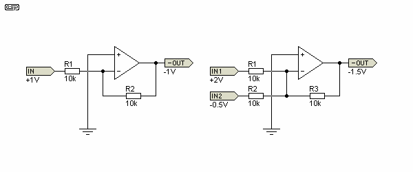
Figure 25 - Summing Amplifiers
By changing the value of R2 (relative to R1), we can modify the gain, making the output voltage larger or smaller in absolute magnitude than the input. It's all done with current - no smoke or mirrors required. Now, if we add another input as shown in the diagram to the right, we can apply another signal, and the opamp will give us a result that is the sum of the two input currents (or voltages, if fixed value resistors are used).
As shown, if one input has an instantaneous voltage of 2V, and the other is -0.5V, the output voltage will be the (inverted) sum of the two - in this case -1.5V. If both inputs were the same voltage and polarity, they are simply added together. At the other extreme, two input voltages of equal magnitude but opposite polarity will result in an output voltage of zero.
There is a drawback to this circuit though, and it is important to understand what happens when you have a large number of inputs. Think back to the inverting amp as originally described. The voltage gain is described by the formula ...
Av = RFB / RIN
We may decide to use several (let's assume 10 for the moment) inputs, all 10k, and all being fed with voltages from different sources (think in terms of a multi-channel mixer). For each input individually, the voltage gain is as described - i.e. -1 (unity, but inverted). What does the opamp see though? The total value of RIN is 10 x 10k resistors in parallel ... 1k. The opamp therefore acts exactly as if it had a gain of 10, so input transistor noise is multiplied by 10, offset current is multiplied by 10, and bandwidth is reduced accordingly.
A small DC voltage shift caused by input offset current (the difference in current needed by each opamp input), is fine for audio. Any DC error is easily removed by adding a capacitor in series with the output. For instrumentation, the DC value may be critical, and this is why some opamps have 'offset null' pins. The designer can use a pot to adjust the offset to ensure that any DC error is 'nulled' out.
While 10 inputs is not going to cause a major problem in most cases, there is often a need for a great many more - a 32 channel mixer will need to be able to sum 32 channels, so the opamp will have a 'noise gain' of 32, even though the gain for each input individually is -1. Note that there is no polarity for noise gain - noise is random in nature, and not correlated to the input signal. Noise is noise.
The opamp also acts as if it were operating with a gain that is equal to the noise gain, even though each input individually has unity gain. As a result, the bandwidth may be (apparently) inexplicably limited, but by knowing the noise gain, we can treat the circuit as if it has a voltage gain that equals the noise gain - and indeed, this is exactly the case.
The inverting amplifier stage is actually noisier than a non-inverting stage with the same gain. For a non-inverting amplifier, the noise gain is equal to the voltage gain, but with an inverting stage, noise gain is equal to voltage gain + 1. When a large number of inputs is needed, a summing amplifier needs to have very low noise and wide bandwidth, or performance will not be as expected.
Because filters are so important in audio, it is necessary to examine a few more variations. Two additional functions will be examined - integration and differentiation. Although Part II did not make it clear, these are the building blocks of some of the most interesting filters that can be made using opamps. A simple integrator (low pass filter) and differentiator (high pass filter) are shown in Figure 26. These are conceptual - the real world nature of opamps means that neither will work as a 'perfect' device, but must be limited to a defined frequency range. In reality, this is rarely an issue, since ideal versions of the circuits are not needed to cover the audio bandwidth.
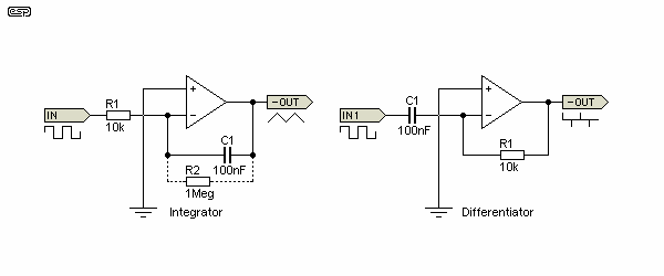
Figure 26 - Ideal Integrator and Differentiator
The differentiator will actually work as shown (albeit with less than ideal performance), but the integrator will not. The reason is simple - it has no DC feedback path, and will drift towards one supply or the other (depending on the opamp characteristics). To combat this, a resistor is needed in parallel with C1 (R2, shown dotted), with a value sufficiently low to provide DC feedback, but not so low as to cause the lowest frequency of interest to be affected. As always, compromises are a part of life.
With an input waveform of a square wave as shown, an integrator provides an output that is dependent on the input current (via R1) and the value of C1. Over a useful frequency range, the output of an integrator is an almost perfect sawtooth waveform with a squarewave input. The DC stability resistor (R2) ultimately limits the lowest usable frequency. While there are methods to get around this limitation, this level of complexity is not normally needed for audio.
The differentiator as shown is also supplied with a squarewave. The output is now based entirely on the rate of change of the input signal, so a squarewave with relatively slow rise and fall times will give a lower output than another with very fast transitions.
The integrator is a low pass filter, with a theoretical 6dB/octave rolloff starting from DC (where it has infinite gain). The 6dB/octave rolloff continues for as far as the opamp characteristics will allow. At an infinite frequency, gain is zero.
A differentiator is the exact opposite of an integrator. It has zero gain at DC, and an infinite gain at an infinite frequency. The filter slope is again 6dB/octave. With ideal opamps, if the two circuits were connected together the output is a squarewave - identical in all respects to the applied signal. With the values shown, the unity gain frequency is 159Hz ( 1 / 2π R1 C1 ).
To see integrators at work in a real circuit, you need look no further than the Project 48 subwoofer equaliser. Differentiators abound in all audio circuits, but in a rather crude form. Every capacitor that is used for signal coupling is a very basic differentiation circuit, in conjunction with the following load impedance. Note that the frequency where coupling circuits will actually function as a differentiator is well below the lowest frequency in audio.
A rather annoying problem exists with integrators. Opamps have input current (even those with FET inputs), and the circuit cannot tell the difference between an actual input current and that caused by the opamp's input stage. Left to their own devices, all integrators will suffer from drift, which is usually temperature dependent. This issue was 'solved' in Figure 26 by the addition of a resistor (shown with dashed connections). However, this is only a partial fix, and if you need a true integrator you'll need to apply a reset at regular intervals. In this case, the reset is achieved by discharging the capacitor. This can be a physical switch, a JFET used as a switch, or some other mechanism. It will usually be triggered by a level detector.
This means that the process of integration is often a very basic analogue to digital converter, with the frequency of reset pulses providing the information about the input current. High input current (or voltage if fed via a resistor) causes rapid resets, and low currents cause them to be less frequent. Opamp selection is critical, and there are highly specialised devices that are designed to provide usable performance. Without a reset, all integrators will eventually drift to one or the other supply voltage. This may take minutes, hours or days, depending on the opamp and capacitor. Even PCB leakage can cause issues when trying to create a long-term integrator operating from low input currents.
In contrast, differentiators are usually well behaved, provided the input rate-of-change (ΔV/ΔT or DV/DT) is within the bandwidth of the opamp. If you have a very fast voltage change, the opamp also needs to be very fast to keep pace with the signal. If the input changes faster than the opamp's reaction time, then the output is inaccurate, and fails to show the rise/ fall time of the input signal.
These functions are mentioned here only because a basic understanding of the principles is a part of understanding filters - most are based on one or the other function, and bandpass filters use both integration and differentiation. Integration in particular is used in the State-Variable filter (described next), and the problem of drift is solved by the nested feedback loops. This isn't normally applicable for 'true' (or stand-alone') integrator circuits.
The State Variable filter is probably one of the most interesting of all opamp filters. It uses nested feedback loops and a pair of integrators to define the filter Q, frequency and gain. Gain and Q are independently adjustable in the version shown - changing R1 will change the Q, but leave the overall gain unchanged. The gain from the bandpass output does change with the Q, something that must be taken into consideration for high Q implementations. A standardised version is shown in Figure 27, and with the values shown, passband gain is unity, Q is 0.707 and the centre frequency is 159Hz (set by R6, C1 and R7, C2). There is a complete article discussing this topology - see State Variable Filters.
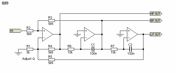
Figure 27 - State Variable Filter
As shown, the filter outputs low pass, band pass and high pass responses simultaneously. R1 sets the filter Q and the amplitude of the bandpass output, and is selected as ...
R1 = 4.98 k (Butterworth - Q = 0.707)
R1 = 11.2 k (Linkwitz-Riley - Q = 0.5)
To calculate for a different Q, use the formula ...
D = 3 × ( R1 / ( R1 + R5 )) where 'D' is damping
Q = 1 / D
The damping is set at 1.414 in Figure 27, giving a Q of 0.707, so the filter response is Butterworth (maximally flat amplitude). The frequency is changed by varying R6 and R7, or C1 and C2. A very common use for the state variable filter is in parametric equalisers, where a filter with variable frequency and Q is a requirement. The state variable filter allows the gain to be changed without affecting Q (and vice versa), so it is an ideal variable filter for audio use. Filter Q remains constant with frequency, so altering the frequency has no effect on the filter's overall (summed) response. Note that the high and low pass sections have opposite polarities, with the high pass shifted by -90° and low pass shifted +90° at the tuned frequency (fo). The bandpass output is in phase with the input at fo
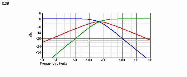
Figure 28 - State Variable Filter Frequency Response
The red trace is the band pass response, the blue trace is low pass, and green is the high pass. Remember that all of these are reproduced simultaneously, thus making the state variable filter on of the most interesting and versatile applications available. The standard state variable filter is second order, having rolloff slopes of 12dB/octave. It is also possible to make these filters with third order (18dB/octave) or fourth order (24dB/octave) response, but that is beyond the scope of this article. A first order state variable filter is also possible, but as far as I'm aware I have the only published version of this circuit (see State Variable Filters). The only other version I know of is from THAT Corporation, who published a voltage controlled version - VCA-Controlled 1st Order State Variable Filter, using the THAT2180 VCA (voltage controlled amplifier).
A variation of the state variable is called a Bi-Quad (aka biquad or bi-quadratic). The difference between the two is subtle. With a bi-quad, as frequency changes, the bandwidth remains constant, which means that the Q must change. As you change the frequency, Q increases as frequency increases and vice versa. Outputs are low pass and bandpass (no high pass), but the Q can be be higher than available with the state-variable. It's not as useful as the state-variable filter and is not shown here.
The bandpass version of this class of filter has its own page on the ESP site - see Multiple Feedback Bandpass Filter for more information about this category. There are also low and high pass versions of the MFB filter, and these will be covered briefly here. The chief advantage of the MFB filter is that the opamp's gain bandwidth product (GBP) is relaxed somewhat compared to the Sallen-Key topology. This is not normally a problem at audio frequencies and for audio applications, because very high Q values are rarely used.
Where the Sallen-Key filter requires a minimum open loop gain of 90Q² at the filter frequency, the MFB version requires only 20Q². To put this into perspective, a Sallen-Key filter with a Q of 0.707 at 20kHz requires an opamp open loop gain of at least 75 at 20kHz, while the equivalent MFB filter only needs a gain of 17 (close enough). While these figures are easy to obtain at low Q values, they become difficult or impossible if a high Q filter is needed.
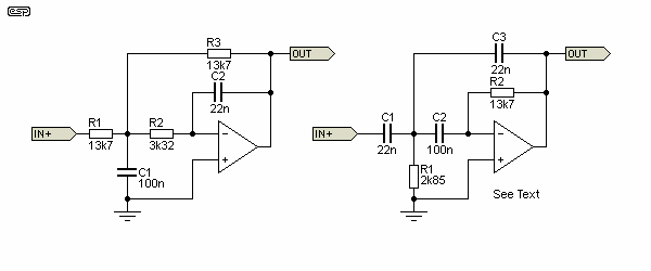
Figure 29 - Low-Pass and High-Pass Multiple Feedback Filters
The first thing to notice with these filters - the resistor (and to a lesser extent the capacitor) values are decidedly non-standard. The design formulae are also rather complex, and I eventually settled on the values shown based on a simulation. The calculations are tedious, and will invariably yield non-standard values. Simple parallel or series connections often cannot be used to get the values you need (based on others in the circuit).
There are several articles on the Web covering the low pass multiple feedback filter, but few that cover the high pass version. As a result, I didn't even try to calculate the values, but figured them out based on the low pass version. As shown, the low pass filter has a cutoff frequency of 503Hz, and the high pass filter has a cutoff frequency of 538Hz. Both have a Q of 0.707 (Butterworth response) and unity gain in the passband.
However, the high pass multiple feedback filter has a fatal flaw, and it's very hard to recommend it for anything. The input impedance is capacitive, which may cause many source opamps to oscillate. In addition, the capacitive load on the inverting input can give rise to instability of the filter opamp. One solution is to add resistance in series with C1 and C2, but this needlessly increases the component count for a circuit that's already only marginally useful. See Active Filters, Section 4 for a more complete description of the issues created by the high pass MFB filter.
As filters, they function exactly the same as any other topology with the same cutoff frequency and Q, but as noted above are less demanding of the opamp performance (low pass only!). Whether this ever becomes a problem for most audio frequency circuits is debatable. Note too that they are inverting, so if absolute phase is your goal, you will need to re-invert the outputs.
There is an almost infinite range of filter types, some are useful, others less so. An interesting idea was described in an online design website. The article, entitled "Bandpass filter features adjustable Q and constant maximum gain" showed an active notch filter followed by a difference amplifier (balanced input stage). The original used to be available on the EDN website but the original link was broken. (There is now a PDF version here). The circuit detail is reproduced below.
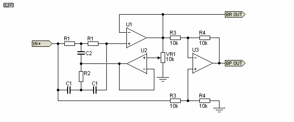
Figure 30 - Notch Filter Followed By Difference Amp
Note that all resistors and capacitors with the same designation are the same value. The 'BP' output is bandpass, and the 'BR' output is band reject (notch).
The notch filter is formed by R1, R2, C1 and C2, where R2 = R1 / 2 and C2 = C1 × 2. The output is buffered by U1, and U2 provides a low impedance feedback path to the notch filter, based on the level set by VR1. U3 is a conventional balanced amplifier, in this case being used as a difference amp. By subtracting the notch signal from the input signal, the result is a bandpass response. The output of the filter can never reach the same Q as the notch however, because phase shift reduces the attenuation of out of band signals.
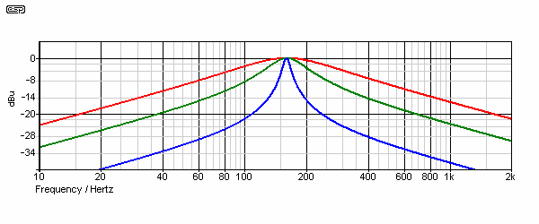
Figure 31A - Bandpass Response
The response with the pot (VR1) set at three levels is shown. The red trace shows the response with VR1 set to 80%, green at 90% and blue at 98%. Useful values of Q (for this type of filter) are only available with close to maximum feedback, but the circuit works as described.
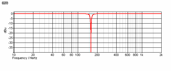
Figure 31B - Band Reject (Notch) Response
The notch filter response (shown in Figure 31B) is as one expects from the twin-tee circuit when feedback is applied. The notch itself is almost infinitely deep, and extremely narrow because of the feedback. The response shown was taken with VR1 set to 98% of its travel - almost maximum feedback applied. Applying more feedback is rather pointless, and the simulator decides that it cannot resolve the notch at all at higher pot settings. The extreme sharpness of notch (band stop) filters in general cannot easily be matched by band pass types. This is largely due to the laws of physics and the way phase shifted signals add together.
The above is another example of the huge range of possibilities for filters - there are obviously a great many more, but space (and usefulness for audio applications) preclude me from going any further in this direction. A web search will reveal many more, and there are also switched capacitor filters, digital filters and perhaps even others not yet invented.
Opamps have limited output current, usually only around 20mA or so. While this is usually more than enough for preamps and filters, a great deal more is needed to drive a loudspeaker. There are several power amplifiers that are configured in exactly the same way as an opamp, and these can be classified as 'power opamps'. While this is often a good way to get the extra current needed, in some cases it may not be considered appropriate or convenient.
Opamps also have a limited voltage swing, and operating them at the voltages typical for power amplifiers will cause failure. While there are already several opamp based amplifiers on the ESP site (as headphone amps, a small power amp, and two power opamps), the following design is different.
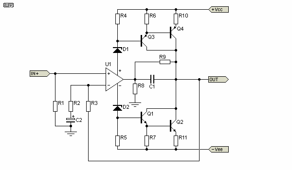
Figure 32 - Power Amplifier Concept
The circuit shown in Figure 32 is conceptional (that's why there are no component values). At one stage, this circuit was quite common, but had some major high frequency issues, as well as DC stability and a host of other problems. Although I do not recommend that anyone even attempt to build it, the circuit is nonetheless interesting. By using the opamp supply current to modulate the transistors base current, the opamp could operate with voltages well above the normal allowed supply voltages, because the zener diodes reduced the voltage to within the allowable range. R9 was included because many years ago (when I actually contemplated using the design), it was found to work better with this in place.
Although my simulator has difficulties with the circuit, it is possible to get it to run with low output voltages. It shows low distortion, but I know from experience that this is dubious - measured (versus theoretical) distortion is higher than expected, and if I recall correctly, somewhat load dependent. Bias current stability can be very poor. This can lead to thermal runaway in the output stage, and it is very difficult to ensure good thermal stability without additional circuitry.
For other power amplifier designs that do work, just look through the ESP projects pages.
All in all, the specifications for even a fairly basic opamp can be daunting. There are so many terms used that it is difficult to understand what they all mean. The easiest are the absolute maximum values - these are simply a set of parameters that should never be exceeded. Supply voltage, input voltage, operating and storage temperatures are just a few of the figures quoted.
Let's have a look at the data for the TL072, chosen because it is still a good general purpose opamp ...
| Abridged electrical characteristics, VCC = ±15 V, TA = 25°C | ||||||
| Parameter | Test Conditions |
|
Units | |||
| VIO Input offset voltage | VO = 0, Rs = 50Ω |
| mV | |||
| αVIO Temp. coefficient of input offset voltage | VO = 0, Rs = 50Ω |
| µV / °C | |||
| IIO Input offset current | VO=0 |
| pA | |||
| IB Input bias current | VO = 0 |
| pA | |||
| VICR Input common mode voltage |
| V | ||||
| VOM Maximum peak output voltage | RL = 10kΩ |
| V | |||
| AVD Large signal voltage amplification | VO = 10V, RL ≥ 2kΩ |
| V / mV | |||
| B1 Unity gain bandwidth | VO = 10V, RL ≥ 2kΩ |
| MHz | |||
| rIN Input resistance |
| MΩ | ||||
| CMRR Common mode rejection ratio | VIC = VICRmin, VO = 0, Rs = 50 Ω |
| dB | |||
| kSVR Power supply rejection ratio | VIC = VICRmin, VO = 0, Rs = 50 Ω |
| dB | |||
| ICC Supply current (each amplifier) | VO = 0, No load |
| mA | |||
| VO1/ VO2 Crosstalk attenuation | AVD = 100 |
| dB | |||
| SR Slew rate at unity gain | VI = 10V, CL = 100 pF, RL = 2 k Ω |
| V/us | |||
| tr Rise time overshoot factor | VI = 20mV, CL = 100 pF, RL = 2 k Ω |
| ||||
| Vn Equivalent input noise voltage | Rs = 20Ω, f = 10Hz - 10kHz |
| µV | |||
| THD Total harmonic distortion | VIrms = 6V, AVD = 1, RL ≥ 2k Ω, RS ≤ 1k Ω, f = 1kHz |
| ||||
Well, it certainly does look rather daunting, so we'll look at each parameter in turn to see what it means. It must be understood that there are many different ways to specify an opamp, and the table above is intended to be representative only.
VIO Input Offset Voltage This is a measure of the typical voltage difference that may exist between the inputs when the first Rule is applied. So, while an ideal opamp will try to make both inputs exactly the same voltage, in a real opamp it may differ by this amount. A TL072 connected as a unity gain buffer with zero input could have between 3 and 10mV between the two inputs (plus or minus). This is measured with zero volts at the output, and a source resistance of 50 ohms.
αVIO TempCo of Input Offset Voltage All real devices are affected by temperature, so the input offset voltage may vary by the amount shown as the operating temperature changes. This figure can be ignored for most audio applications. It is important for instrumentation amplifiers, high gain DC amplifiers and other critical applications.
IIO Input Offset Current The input current will change with temperature, and the two input devices may not match. Offset current is primarily caused by gate leakage. The value is very small for FET input opamps, having a maximum value of only 100pA for the TL072.
Ib Input Bias Current Even though the TL072 is a FET input opamp, it has some input current, primarily caused by gate leakage. The current is very small, ranging from 65pA to 200pA.
VICR Input Common Mode Voltage This is often an important parameter, and is very much so with the TL07x series. If exceeded, the output state becomes undefined. In the case of the TL07x devices, there can be a change of state of the output voltage if the input common mode voltage is exceeded. A signal that should just clip has a sudden transition to the opposite polarity during the period where the common mode voltage is exceeded. A few other opamps have a similar problem, but most do not.
VOM Maximum Peak Output Voltage Few opamps can swing their outputs to the supply rails, and the amount of current drawn from the output affects this further. This limitation is only apparent when using low impedance loads, although there is still some loss with no load at all. By using the highest (sensible) supply voltage, this is not normally a problem.
AVD Large Signal Voltage Amplification This is usually the open loop (no feedback) condition, and is a measure of the maximum gain of the opamp for high level outputs. At a minimum of 25V / mV, this represents a gain of 25 / 0.001 = 25,000 (it is typically as high as 200,000 or 106dB at low frequencies). This is rarely a limiting value in any audio circuit.
B1 Unity Gain Bandwidth The frequency at which the opamp's open loop gain falls to unity is the unity gain bandwidth. When feedback is applied, it is usually desirable to have at least 10 times the gain that you specify with the feedback components. This represents an error of ~10% at the upper frequency. Unity gain bandwidth limits the maximum gain you can use for a given upper frequency.
rIN Input Resistance The input voltage divided by the input current (Ohm's law). So with an input voltage of 1V and an input current of 65pA, the input resistance is 153GΩ. The exact derivation of the value claimed in the table is unclear, since the measurement conditions are unspecified. Many datasheets state the input resistance of TL07x series to be 1TΩ (1,000 GΩ)
CMRR Common Mode Rejection Ratio A measure of how well the opamp rejects signals applied to both inputs simultaneously. See the description of the balanced input stage for more information. Common mode rejection depends on the available open loop gain, and deteriorates at higher frequencies. This is graphed in most data sheets.
kSVR Power Supply Rejection Ratio All opamps can have some noise on the supply lines without serious degradation of the signal. PSRR is a measure of how well the opamp rejects (ignores) the supply noise or other unwanted signal(s) that may be carried by the supply buses.
ICC Supply Current (Each Amplifier) Needless to say, some current is drawn by all opamps. This is simply the typical current you expect to draw from the supply for each opamp in the package. At 1.4mA per opamp, a dual (TL072) will typically draw 2.8mA with 15V supplies.
VO1/ VO2 Crosstalk attenuation When there are two or more opamps in a package, it is inevitable that some signal will pass from one to the other. As specified, this will be -120dB if the amplifiers are operating with a gain of 100. In general, PCB layout and circuit wiring causes far more crosstalk than the IC itself.
SR Slew rate at unity gain The slew rate is simply how fast the output voltage can change. The specification says that this is measured with the opamp connected as a non-inverting unity gain buffer. In this case, the opamps is specified for a typical slew rate of 13V/us, meaning that in one microsecond, the output voltage can change by 13V. There are faster and slower opamps of course, but for audio work it is actually difficult to exceed the slew rate of any but the slowest opamps.
tr Rise time overshoot factor When any electronic circuit is subjected to a very sudden change of input voltage, the opamp will often not be fast enough to maintain control via the feedback loop. Once control is lost, there is a finite time before the opamp 'catches up' to the input signal. This causes the output to overshoot the steady state level for a brief period, and the overshoot is measured as a percentage of the voltage change.
Vn Equivalent input noise voltage This is a theoretical noise voltage that lives at the opamp's input. This noise is amplified by the gain that is set for the circuit. In this case, if the amp is designed to have a gain of 10, the output noise will be 40µV, over the frequency range of 10Hz to 10kHz. Noise is also expressed as nV√Hz (see separate article).
THD Total Harmonic Distortion This is pretty much self explanatory. The test conditions are not always representative of real world application, but in this case appear to be reasonably sensible. The use of a unity gain amplifier is not the choice I'd make, but I didn't design the test specification. 
The data above is based on National Semiconductor's data sheet and terminology. Other manufacturers may choose to use different terms for the parameters, use different test methods, or specify different operating conditions for the same test. The only way you will get to understand the terminology used is to read it - don't just look at it as gobbledygook and ignore it - you will never learn anything that way.
Comparators are so important in electronics that they have their own page on the ESP site. See Comparators, The Unsung Heroes Of Electronics for a lot more information on these essential building blocks. Note that comparators always follow my opamp Rule #2 (which states that 'the output will produce a voltage that has the same polarity as the most positive input'). If the inverting input is the most positive, the output will be at the negative supply voltage (which may be the same as earth/ ground - zero volts).
The poor comparator is the (almost) forgotten first cousin of the opamp. Although comparators are very similar to opamps, their design is based on the fact that they will never have negative feedback applied (although positive feedback is not uncommon!). Consequently, there are no constraints set by the necessity for stability with gain reduction caused by applied feedback. Although opamps can be used as comparators in low frequency applications, they are totally unsuitable at high frequencies. This is because of the frequency compensation applied in opamps, necessary to maintain closed loop (negative feedback) stability.
Because this restriction is removed for true comparators, they are able to be much faster than opamps, although it can still sometimes be a challenge to find a comparator that is fast enough if the operating frequency is high. Class-D amplifiers rely on a fast comparator to convert the analogue input signal into a pulse width modulated switching signal, and they need to be very fast indeed if timing errors are to be avoided.
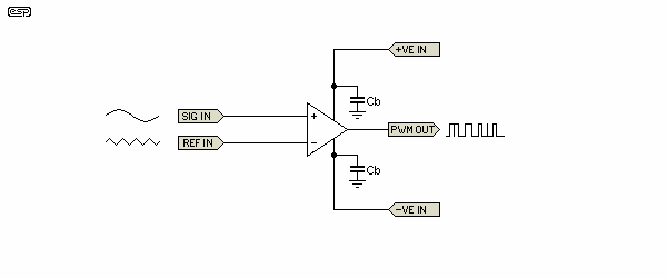
Figure 33 - PWM Comparator
Figure 33 shows the general idea for a pulse width modulator. The input sinewave is compared to the reference signal - usually a very linear sawtooth waveform. Since typical PWM amplifiers operate at a switching frequency of 250kHz or more, even a few nano-seconds switching delay becomes significant, but there are other applications where even faster operation is desirable.
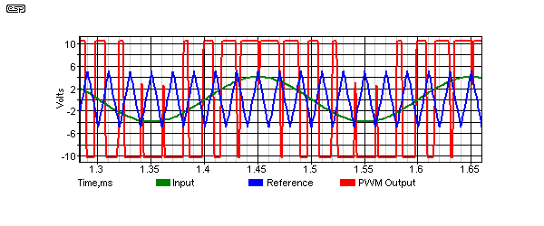
Figure 34 - PWM Comparator Waveforms
The PWM waveforms are shown above. A perfect example of the speed limitation is visible as the input signal approaches the peak value of the reference signal. The comparator is simply not fast enough to switch from one extreme to the other, resulting in the loss of pulses. This is a real phenomenon, and occurs with all PWM amplifiers as they approach clipping.
Achieving very high speed is a compromise, because high speed means that all circuit impedances must be low, thus increasing supply current. This means that the parts will get hot, unless the supply voltage is limited. For exactly the same reasons, microprocessor ICs are now using 3.3V instead of 5V, and high speed digital logic chips are all limited to 5V supplies. We can expect to see the voltage decrease even further as the speed of digital systems increases.
Needless to say, PWM amps are not the only place comparators are used in audio. LED meter ICs have a string of comparators, they may be used for basic (or precision) timing applications, clipping detectors, etc. Most analogue to digital converters use comparators as well. While you don't see them much in linear audio circuits, they are very common in industrial process control systems, and they are a very important 'building block' for many circuits.
Because they have no feedback, comparators always obey the second rule of opamps ... the output takes the polarity of the more positive input. Look carefully at the PWM waveform shown above, and you will see exactly that. Look closely - it is not immediately apparent, but it is visible.
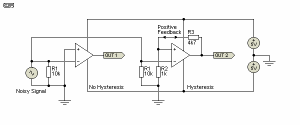
Figure 35 - Comparator Circuits
Comparators can be absolute, meaning that the output will change state whenever the signal passes the threshold. While this is needed for analogue to digital conversion and many other applications, it is often preferable to arrange the circuit so it has 'hysteresis'. This is a rather odd concept, but means that once the signal has caused an output change, it needs to change further (in the opposite direction) to cause a reversal. For example, a comparator may change its output state (e.g. from low to high) when the voltage reaches 5V, but it may have to fall to 4.5V before it changes state again (from high back to low). Hysteresis can be likened to the snap-action of most switches, and indeed, these use mechanical hysteresis.
Both circuits are shown above and the waveforms are shown below. Note that both comparators are shown as inverting, because this connection provides the highest input impedance when hysteresis is added. If a non-inverting connection is used the input would be applied to the +ve input, via R2 for the version with hysteresis, and the -ve input connected to the reference voltage - in both cases this is ground (zero Volts). In a non-inverting connection, the positive feedback will create distortion on the input waveform - this can be a problem if the signal is intended to be used as an analogue waveform elsewhere in the circuit.
The polarity of any comparator can be reversed with a digital logic inverter, another comparator, or the input can be buffered to prevent positive feedback artifacts from being added to the signal. As always, there are many, many ways to achieve the same result, and the final circuit depends on your specific needs.
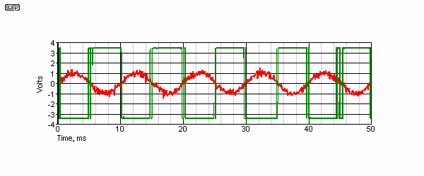
Figure 36 - Comparator Waveform Without Hysteresis
As you can see from the above diagram, if a noisy signal is applied to the input of an absolute (no hysteresis) comparator, the output shows multiple state changes as the input signal passes through zero. This happens because the noise amplitude is enough to cause the instantaneous input amplitude to pass through zero multiple times at each zero crossing of the input signal. This is usually undesirable, because comparators are commonly used to convert input waveforms into a digital representation, based on zero crossings of the input. Multiple triggerings as shown will cause an erroneous output. However, hysteresis is generally not used when converting a waveform to PWM, because the hysteresis may cause unacceptable distortion in the demodulated output waveform.
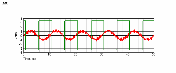
Figure 37 - Comparator Waveform With Hysteresis
Figure 37 shows the input and output waveforms of the comparator with hysteresis. The noise is ignored, because once the comparator changes state, the signal must go negative by more than the hysteresis voltage before it will change state again. The amount of hysteresis is determined by R2 and R3, and may be calculated to give a specific (and exact) level before the output will change state. This circuit is also known as a Schmitt (or Schmidt) Trigger, and is a very common circuit. It is used in the PCB version of P39 (power transformer soft-start) to ensure accurate timing without any possibility of relay chatter as the timing voltage reaches the trigger point.
Calculating the trigger voltages for the inverting case is easy (see below), but is somewhat more irksome for the non-inverting configuration because the input and output voltages interact, even when the signal source has very low impedance. Only the inverting is described here. R2 and R3 form a simple voltage divider. When the output is high (+3.5V), the voltage at the +ve input is ...
Vd = ( R3 / R2 ) + 1 = ( 4.7k / 1k ) + 1 = 5.7 (where Vd is voltage division)
Vin = Vout / Vd = 3.5 / 5.7 = 614mV
The signal therefore must exceed +614mV before the output will swing negative. When it does, the input then has to exceed (become more negative than) -614mV before the output will change state again, because the circuit is symmetrical. Any signal that does not reach the ±614mV thresholds will not cause the output to change state - such signals are completely ignored.
It is also possible (and not uncommon) to make the trigger thresholds asymmetrical, and I shall leave this as an exercise for the reader to work out how this can be done. (Hint - diodes are commonly used to do just this).
This is but a small sample of comparator applications. They may well be the almost forgotten first cousin of opamps for the beginner or novice, but are extensively used in all kinds of circuitry - not necessarily audio, but they are very common there too. Most comparator applications are easy enough to understand once you have the basics, and this section is intended to provide just that - the basics.
Although the three articles in this series have only scratched the surface, hopefully you will have sufficient information as to how opamps work to be able to analyse any new circuit you come across. There is no doubt that there will be some applications that will cause pain, and it is completely impossible to make it otherwise.
Even though there are three fairly large pages devoted to the topic here, there are countless other applications for opamps - not only in audio, but in instrumentation, medical applications, and any number of industrial processing systems. There is almost no analogue application these days that does not use opamps, although in many cases you may not be aware they are there. Opamps and/or comparators are embedded in many other devices, from analogue to digital converters (ADCs) and digital to analogue converters (DACs), digital signal processing (DSP) ICs, switchmode power supply controllers - the list is endless.
I have used various references while compiling this article, with most coming from my own accumulated knowledge. Some of this accumulated knowledge is directly due to the following publications:
National Semiconductor Linear Applications (I and II), published by National Semiconductor
National Semiconductor Audio Handbook, published by National Semiconductor
IC Op-Amp Cookbook - Walter G Jung (1974), published by Howard W Sams & Co., Inc. ISBN 0-672-20969-1
Active Filter Cookbook - Don Lancaster (1979), published by Howard W Sams & Co., Inc. ISBN 0-672-21168-8
Data sheets from National Semiconductor, Texas Instruments, Burr-Brown, Analog Devices, Philips and many others.
The TL07x data sheets from National Semiconductor was extensively referenced in the basic specifications section.
Cirrus Logic, Application Note 48
Bandpass filter features adjustable Q and constant maximum gain - EDN (Local Document)Recommended Reading
Opamps For Everyone - by Ron Mancini, Editor in Chief, Texas Instruments, Sep 2001
Main Index
Articles Index