

|
| Elliott Sound Products | FETs & MOSFETs |
 Main Index
 Articles Index
JFETs (junction field effect transistors) have been with us for many years now, and there was a time when there were many different types available, often with some very desirable characteristics. JFETs became readily available about 10 years after BJTs (bipolar junction transistors), and were quickly adopted for applications that required high impedance inputs. BJTs require an input current to conduct, and that means that they also require current from the signal source to change their output current. While the current is usually very low, it does cause problems in some cases. MOSFETs (metal oxide semiconductor field effect transistors) came along a bit later, and revolutionised high speed switching.
FETs (both JFETs and MOSFETs) are voltage controlled, and require no (static) current from the signal source. However this only applies with DC, because gate capacitance has to be considered for AC. All JFETs are unique amongst semiconductor devices, in that they conduct more-or-less equally in both directions (i.e. both 'normally' and with drain and source interchanged). A BJT will (perhaps surprisingly) work with emitter and collector reversed too, but the gain of modern devices is very low in this mode - sometimes less than unity. FETs can be thought of as a voltage controlled resistor, and this is exploited in many different ways.
Unfortunately, the resistance is not linear. It varies with current, and although the effective resistance can be changed by varying the gate voltage, that relationship isn't linear either. Claims that FETs are more linear that BJTs must be treated with suspicion, because in most cases it's simply not true. Similar claims are made for valves (vacuum tubes), and they aren't true either.
MOSFETs conduct in both directions too, but they have an intrinsic body diode that will conduct when the reverse voltage exceeds around 600mV peak. This means that they cannot be operated as a linear amplifier if the drain and source are interchanged. Nor are they useful as a voltage controlled resistor, because the body diode will conduct if the peak voltage exceeds 600mV. Even if the voltage is kept well below 600mV (peak - about 325mV RMS sinewave), linearity is very poor. However, MOSFETs can make very good audio switches if configured properly.
Unfortunately, the range of available JFETs has shrunk alarmingly in the last few years. Most of the devices that were used for very low noise circuitry are no longer available, and those you can still get from major suppliers are far less useful than the 2SK170 and its ilk. While you can (allegedly) get the 2SK170 or similar from ebay (mainly from Chinese suppliers), the chances of them being the real thing are not good. It's far more likely that you'll get something far more pedestrian, but re-labelled. The LSK170 (made by Linear Systems) is an equivalent, and is currently available, although distribution is patchy.
Some typical FET applications are as follows ...
These applications will be covered in more detail below.
Most of the JFET circuits and simulations shown here are based on the BF256B - not because it's anything special, but because it's still was readily available for a reasonable price. It's intended as an RF amplifier, but that doesn't preclude audio in any way. Like any active device, FETs work from DC up to a frequency determined by the specific characteristics of the device itself - whether by design or accident.
There are also a number of comparisons made between JFET/ MOSFET and BJT circuits. In many cases, this is not flattering to JFETs as their performance is often well below that for a circuit with similar performance based on common bipolar transistors. This is not intended to discourage the use of JFETs at all, nor to suggest that they are 'inferior'. They are different, and it's important to understand the differences between the two parts. However, if you don't need very high input impedance, BJTs will usually give better results than FETs.
One of the reasons that BJTs are so popular is that they have one parameter that is extremely predictable - the base-emitter voltage. This is normally taken to be 0.7V (sometimes 0.65V), and it's the same for small signal and power devices, and is still correct for PNP or NPN. This makes them very simple to bias, but more importantly makes it fairly easy to calculate the gain of a stage. Because BJTs have high transconductance and an exceptionally high collector impedance, it's possible to set the gain with only a pair of resistors. This isn't really possible with JFETs (it can be done, but the gain is not determined solely by the resistor values). It is almost possible with MOSFETs due to their much higher transconductance.
In the following article, only N-Channel JFETs and MOSFETs are discussed. P-Channel versions work in the same way, but naturally require the supply polarity to be changed. Fully complementary designs (including linear CMOS - complementary MOSFETs) are not shown, because they are a rather different application. Also, output coupling capacitors are not shown. These will be needed in most cases, but were not included for clarity. Input coupling caps are shown when they are required.
There is one other function that is potentially useful for MOSFETs. They make very good high power relays, and this is discussed in the MOSFET Relays article. This mode of operation is not covered here.
One of the things I won't do in this article is explain exactly how a JFET or MOSFET is made. The inner workings are explained on countless websites, and there's no point repeating what is readily available elsewhere. Nor will I go into any detail about how they work at the quantum level, as this is also available from manufacturers and physics sites. What I will do is point out that FETs are voltage operated, and apart from having to charge and discharge the gate capacitance, they do not draw appreciable current from the signal source.
The DC gate current of most FETs is typically measured in nanoamps, and usually can only be measured when the gate-source (or gate-drain) voltage is close to the maximum permissible. A typical figure is around 1nA at 25°C, but as with many other semiconductors it increases at elevated temperatures. The gate capacitance of the average small-signal JFET is around 5-30pF, depending on how the device has been fabricated and the intended usage. JFETs for RF applications will usually have lower capacitance than devices intended for low noise audio (for example). The capacitance is primarily due to the thickness (or otherwise) of the P-N junction that separates the gate from the channel.
Two of the most important parameters for small signal JFETs are the drain-source current (IDSS - current with gate shorted to source) and the 'cutoff' voltage, where the gate voltage closes the conduction channel so only a small defined current flows. This typically varies from 10nA to 100nA, but it depends on the device and the manufacturer. This is called the drain-source cutoff voltage (VGS (off)). You also need to know the maximum Drain-Source voltage (VDS), especially if you intend to run with supply voltages over 15V or so.
The gain/ transconductance of a FET (or MOSFET) is measured in Siemens, with most having rather low gain compared to a BJT. Transconductance is also referred to as 'Forward Transfer Admittance' (written as |Yfs| ) in some datasheets. Transconductance is the same gain terminology used with valves, which are also voltage controlled. It can be difficult to relate to the Siemens as a unit, and it is often easier to convert to mA/V. The early (during the valve era) way to specify transconductance was the 'mho' (ohm spelled backwards), and it's still seen in some FET datasheets. You may also see the mho as a symbol - ℧ - an upside-down Omega.
1 Siemens (1S) is equal to 1 Ampere per Volt, so 1mS is the same as 1,000µmhos, which is 1mmho or 1mA/ Volt. Transconductance of JFETs varies depending on the manufacturing process and the intended application. Typical values will range from around 1mS (1,000µmhos, 1mmho or 1mA/V) to 22mS (22,000µmhos, 22mmho or 22mA/V).
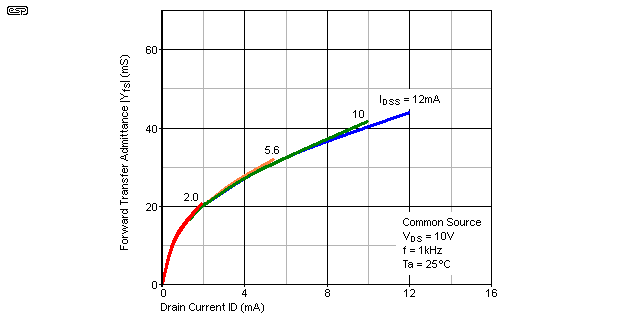
Figure 1 - Transconductance Graph For 2SK170/ LSK170
For reference, the above graph shows the transconductance (actually |Yfs| ) for the 2SK170/ LSK170 (from Linear Systems) low noise JFET. As you can see, the transconductance changes with drain current, so to get low distortion the current should remain constant. This is easily achieved in practice, and the linearisation effect of using a constant current load is also seen with other FETs, BJTs and valves.
Almost all JFETs are what's known as 'depletion mode' devices. This means that they conduct with no gate voltage (typically gate shorted to source or at the same potential). This is the maximum current region, and usually must be avoided for linear operation. The FET is biased off by applying a negative voltage to the gate with respect to the source, and they can be biased in exactly the same way as a valve.
The vast majority of MOSFETs are 'enhancement mode', meaning that a positive voltage is required on the gate (with respect to the source, for an N-Channel device)) to make the MOSFET conduct. There were quite a few depletion mode MOSFETs available many years ago, but they are less common today. They are recommended for constant current sources and MOSFET relays, although their power ratings are typically much lower and on-resistance much higher than enhancement mode MOSFETs. I will not cover depletion mode MOSFETs in any detail, as their usage is generally rather specialised. P-Channel MOSFETs are also predominantly enhancement mode, but depletion mode types are available (albeit fairly uncommon).
Like BJTs, both JFETs and MOSFETs change many of their characteristics with temperature. I'm not going to provide any detail on that, as it's all available in the datasheets. However, it is important to remember that when the temperature of any semiconductor changes, its normal operating conditions will be altered. A robust design ensures that no realistic temperature variation will cause the circuit to malfunction, so proper testing is essential. You don't need an environmental chamber, but you do need to test thoroughly.
Be particularly careful with MOSFETs, because RDS(on) increases as the device gets hotter. While this characteristic helps to force current sharing when MOSFETs are in parallel, it also increases the risk of thermal runaway. Make sure that MOSFETs that dissipate significant power always have a properly sized heatsink to ensure that the temperature can never reach a dangerous level.
One of the less endearing attributes of JFETs is their parameter spread. The IDSS (drain-source current, gate shorted to source) can vary widely, typically with a 5:1 ratio. This means that the same type of JFET could have an IDSS ranging from 1-5mA, with some having an even wider range. Even the somewhat revered 2SK170 has a quoted IDSS range from 2.6 to 20mA - a 7.7:1 ratio. This means that simple biasing techniques don't necessarily work, because all of the performance parameters have similar variations. VGS (off) is the voltage where the drain current is reduced to a specified value, and again using the 2SK170/ LSK170 as an example, this ranges from -0.2 to -1.5V for ID of 0.1µA (100nA).
What this means in a real circuit is that proper biasing can be difficult to achieve unless feedback is used. A JFET will probably work without you having to make circuit changes, but it won't be biased into its most linear point on the transfer curve. This may limit the dynamic range and/or distortion characteristics, so it's almost always necessary to provide at least some degree of adjustment to ensure the best linearity.
Transconductance also varies widely, although in most cases it doesn't change as much as the datasheets might imply. Because the gain of a single FET amplifier stage is far lower than that from a BJT, they are often operated with no local degeneration (as is usually provided by an un-bypassed source resistor). This means that the AC voltage gain varies with the transconductance. In theory, if a JFET has a transconductance of (say) 1mmho (1mS, or 1mA/V) a gate voltage change of 1V will cause the drain current to change by 1mA. Likewise, a change of 10mV will cause the drain current to change by 10µA. If the drain resistor is 10k, that's a voltage change of 100mV across the resistor - a voltage gain of 10.
If another FET of the same type but with a different transconductance is substituted, the gain will be different. These variations in all of the important parameters mean that it can be difficult to get a consistent gain from FET stages in production. This is not to say that it can't be done, nor is it necessarily a problem in reality, but it is important for stereo preamps where good channel balance is expected. These issues can be solved easily enough by using feedback (AC, DC or both).
The parameter spread is not just limited to the device itself. Manufacturers often don't use the same terminology, and some will specify forward transconductance, others show |Yfs| instead. Transconductance may be given in mS (milli-Siemens) or µmhos (sometimes mmhos - millimhos), but few use the more easily understood value in mA/V, which as noted above is the same as mS and mmhos.
In short, all FET parameters vary, some widely, and the designer has to be aware of this if a consistent design is expected at the end of the process. Regular readers will be aware that few ESP projects use discrete FETs. This is due to the likelihood of any given device disappearing from the market after publication, or because the most appropriate FET is simply no longer available. The inherent variability of the basic parameters is the final straw - I don't like to publish circuits that constructors will build, but that fail to work as intended without modification. Sometimes there are simply no alternatives, and the Project 16 - Audio Millivoltmeter is a case in point. There are several alternative devices suggested, and a note that the source resistor will likely need adjustment to set the optimum operating conditions.
This is all rather tiresome, and provided you don't need extended frequency response, a FET input opamp is a far better option if you need very high input impedance. It's also important to understand that despite claims to the contrary, FETs do not provide 'higher resolution' of audio signals, they don't 'sound better' and nor do they somehow (magically perhaps?) improve anything (bass, treble, midrange, 'air' or 'authority') compared to opamps or BJTs. When they are used as amplifiers, they amplify (and distort) just like any other active device, including valves (which are also bereft of 'magic'). Depending of the FET type and usage, there might be a difference (in either direction) in background noise level, but this depends on a great many factors and is not an intrinsic characteristic of FETs over other amplifying devices.
We seem to be operating in some kind of parallel universe sometimes, with some people claiming often huge benefits of one type of amplifying device over the others. Most of this is imagined or the result of personal prejudice, but even major manufacturers can (and do) postulate that their JFET opamp is somehow 'sonically superior' to others. If any amplifying device can amplify an audio signal by a given amount, it will be indistinguishable from any other with the same gain, frequency response, noise and distortion. To claim otherwise is akin to believing in fairies at the bottom of the garden. Some topologies are 'better' than others, but usually only in one or two major parameters. Other parameters may be worse.
I tested a pseudo-random batch of JFETs that had all been set up as constant current sources, with a design current of 4mA. They are 'pseudo-random' in that they all came from the same batch from the supplier, and were removed from the bag and installed with no attempt at grading them. The current was set using a trimpot for each FET. Based on the resistance needed to bias them, their gate-source voltage can be determined for 4mA drain current ...
| Resistance | VGS | Resistance | VGS |
| 662 Ω | 2.65 V | 896 Ω | 3.58 V |
| 644 Ω | 2.58 V | 648 Ω | 2.59 V |
| 633 Ω | 2.53 V | 644 Ω | 2.58 V |
| 665 Ω | 2.66 V | 655 Ω | 2.62 V |
As you can see, most are passably close, but one (yellow shaded cells) is well out of range of the others. This is why a simple biasing scheme can fall apart - the one device that's well outside the specs of the others will also cause its performance to be well outside reasonable bounds, so without making an adjustment the proper operating point will be unpredictable. Even those that are pretty close will create issues if you are building a discrete opamp with JFET inputs (for example). If you don't match the FETs, you could have a DC offset of as much as 1.05 volts with the worst two JFETs shown in the table. If you use the best two, there's no difference There are two with a VGS of 2.58V, but there is no guarantee that this exact match will apply at a different current (hint - it probably won't).
A JFET voltage amplifier stage is easily made, but as noted above the parameter spread can mean that the circuit may need to be tweaked to get the optimum operating point. The gain of a simple JFET amplifier stage is much lower than you can get from an equivalent BJT stage with a similar parts count. Of course, the JFET has a much higher input impedance, and this is often the main reason for using FETs over BJTs. The operating point is important when the minimum possible distortion is required, and simple resistor loading limits the maximum output voltage swing if distortion is to remain within acceptable limits.
With FETs and BJTs in simple circuits, second harmonic distortion is dominant, with lesser amounts of 3rd, 4th, 5th etc. For a given output swing and gain, FETs will almost always have higher distortion. With a BJT stage, the emitter resistor can often be left un-bypassed and the relative values of collector and emitter resistance set the stage gain. Because FETs generally have a much lower gain than BJTs, the source resistor nearly always has to be bypassed or you won't be able to get enough gain from the amplifier stage.
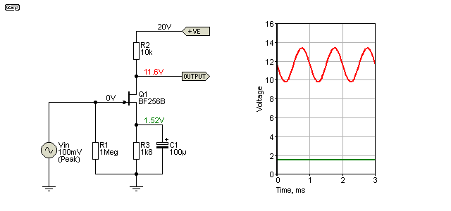
Figure 2 - Basic JFET Common Source Voltage Amplifier Stage
The circuit shown (according to the simulator) has a voltage gain of 17.4 (24.8dB), an input impedance of 1MΩ (purely due to the value of R1) and an output impedance of about 8.6k, a little less than the value of the drain resistor. With a 100mV (peak) input, output is 1.74V peak, and distortion is simulated to be just over 1.4%. If R3 is left un-bypassed (remove C1), the gain falls to 2.5 (8dB), but there will be a noise increase because of the thermal noise of R3 (which is amplified by Q1). C1 is selected so its reactance is no more than 1/10th of the resistance of R3 at the lowest frequency of interest. 68µF is the closest readily available value, but 100µF is preferred, and gives a low frequency -3dB frequency of 3.8Hz.
Note that the source voltage is +1.51V, so the gate is negative with respect to the source via R1 (which holds the gate at ground potential). This is the biasing voltage required to set the drain to somewhere near half the supply voltage. The biasing principles for a depletion mode FET are identical to those used for valves. The bias voltage needed depends on the FET itself - not just the type number, but it may need to be adjusted for individual FETs.
You might have noticed that the -3dB frequency is higher than expected. 100µF and 1.5k has a -3dB frequency of 1Hz, so you would expect that would be the -3dB frequency of the amplifier stage. However, the impedance of the source comes into play, reducing the apparent impedance that has to be bypassed to around 420 ohms. This is also the input impedance if the circuit is operated as common/ grounded gate (a mode that isn't covered in this article, other than in Section 8 below).
Based on the measured output impedance, the effective drain resistance (which is in parallel with R2) can be calculated at 61k. This value isn't useful, but I thought I'd mention it anyway. The DC (quiescent - no signal) operating voltages for the circuit are shown in the same colour used in the graph.
The DC operating point is not necessarily optimum for all parameters. By increasing the current slightly, distortion is reduced and gain is increased, but the drain voltage is reduced and the output will clip asymmetrically. For example, reducing R3 to 1k increases the gain to 19.4 (25.8dB) and reduces distortion to 0.43%. However the drain voltage is only 7.2V and the negative half cycles will clip well before the positive half cycles. This may not matter in a practical circuit of course, but it's a trade-off that you need to be aware of. Other JFETs may behave differently, and the only real way to know is to run tests.
While it is possible to calculate the gain of a simple JFET voltage amp stage, doing so is rather irksome. The process used to calculate the gain of a valve stage can be applied (see Biasing and Gain in the valves section), but JFET datasheets don't include the 'amplification factor' (usually written as µ or 'mu'), nor is the effective drain resistance (equivalent to plate resistance for a valve) specified. Determining the amplification factor is not as easy as it might be, because FET manufacturers don't provide the necessary data.
While it may look easy enough to use the transconductance figure to calculate the gain, it's not as straightforward as it may appear. If a FET has a transconductance of 1mS, this works out to be 1mA/V - meaning that the drain current will (theoretically) change by 1mA for each volt change at the input. While you might imagine that this can be used to calculate the gain, it usually doesn't work. Most of the time, the specific parameters that are needed to calculate the gain have to be measured, and if you set up to do that you can simply measure the gain instead. This is far easier than working out the parameters and calculating the gain, and the end result is also more accurate because you measured it with the device under normal operating conditions. Remember parameter spread - it is not your friend  .
.
To expand on the issue of gain calculation, you must be aware that the transconductance is not a fixed value. It changes depending on the drain current, so it will be quite different at (say) 100µA and 10mA. As an example, you might measure 2mA/V (2mS) at 1mA current, but at 7mA it might be 5.7mA/V (5.7mS). You can't make meaningful calculations with a moving target like that.
Because of the source resistor, there is some tolerance for differing VGS values. The DC operating point (measured at the drain terminal) will change proportionately to the difference in VGS, and it might be enough to cause the circuit to fail to work properly. This is especially true if the operating point is marginal to start with. The circuit will probably still amplify, but may have (perhaps grossly) excessive distortion.
Like all simple single transistor (JFET, MOSFET or BJT) gain stages, power supply rejection is minimal, so a very clean DC supply is essential. Power supply hum or noise will be coupled into the output signal with very little attenuation. The power supply rejection will typically be less than 3dB, so if there's 100mV of noise on the supply, you can expect at least 70mV at the amplifier's output.
Simple FET voltage amps are (or were) fairly common in undemanding applications, but in many cases something a little more refined is needed. A popular configuration is called a 'mu-follower', which uses a second JFET as a bootstrapped load for the amplifier. This improves linearity and increases the gain. There are many variations on the basic idea though, and there is no consensus as to which version is the 'true' mu-follower. While the gain is increased significantly by most of the common schemes, so too is output impedance. This means that the following circuitry must have a very high input impedance, or a voltage follower is needed to reduce Zout (output impedance) to something usable.
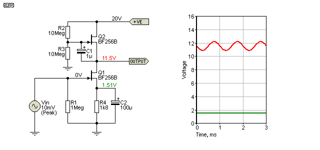
Figure 3 - Mu-Follower Voltage Amplifier
The DC operating conditions are not changed much with this arrangement, but the gain is considerably greater. It may not look like it based on the graphs, but the input is only 10mV peak, where the previous example used a 100mV peak input. Gain is now around 67 (36.7dB) and distortion is 0.78% when the output level is increased to be the same as the previous example (1.74V peak). So, while the gain has been increased significantly (3.8 times), the distortion is only reduced by a factor of 1.8 - worthwhile, but not dramatic. Output impedance is also increased, rising to about 30k. The following stage needs an input impedance of at least 10 times this (300k) or gain will be greatly reduced. Frequency response of the circuit as shown (at the -3dB points) is from 3.1Hz to 775kHz - more than enough for any audio circuit.
Output impedance can be reduced to something more sensible by adding a FET source follower, but a BJT emitter follower is likely to give better results. You may imagine that a MOSFET would be preferable, but it's not necessarily the case - while output impedance is lower than with a BJT, the distortion is higher. A reasonable sized power MOSFET is a little better than something like the 2N7000 (a low current N-Channel MOSFET), but a high gain, small signal BJT usually performs better.
A FET has an almost infinite current gain because the input impedance is so high. The only limitation is the fact that a resistor is needed so the gate is referenced to ground (or a suitable negative voltage with respect to the source). There's no reason that the resistor can't be as high as 1GΩ or more, although PCB leakage may become a problem with such extreme impedance levels. In most cases, an input capacitor is essential, because without it the FET's bias point can't be maintained (the gate would be at zero volts rather than around 8.4V or -1.5V referred to the source - FET dependent). If the source is a piezo-electric transducer a capacitor is not needed, because the piezo element is capacitive and doesn't pass DC. This can be useful for piezo accelerometers for example, but a FET input opamp will usually give better results.
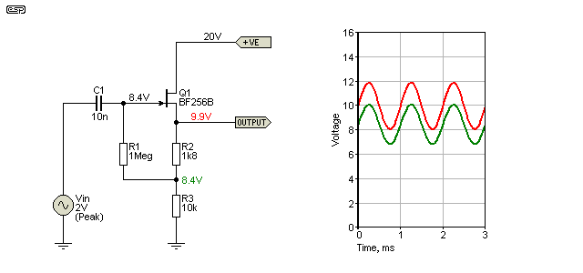
Figure 4 - JFET Source Follower
The overall performance of the circuit can be improved by using a constant current sink in place of R3. With all semiconductors, they are more linear in any topology if the current is maintained at a constant value. This applies equally to voltage or current amplifiers, and with BJTs, FETs (including MOSFETs) and valves. With low signal levels the gain is probably not worth the additional parts and cost, but it obviously depends on what you wish to achieve. As shown, the distortion with a 2V (peak) input signal is 0.05%, but is reduced dramatically with a FET current sink as the load. Performance is improved further with a better current sink, but the law of diminishing returns makes it uneconomical to add to a simple circuit that doesn't even equal a lowly TL071 for audio frequency distortion performance.
Input impedance of the circuit is around 5MΩ because R1 is partially 'bootstrapped' by being joined to the junction of R2 and R3. Input impedance can be increased further (to around 20MΩ) by bypassing R2 with a 100µF capacitor. Gain is not unity - it's about 0.94 due to the low transconductance of the FET. Output impedance is around 400 ohms.
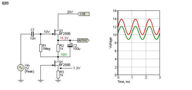
Figure 4A - Improved JFET Source Follower
As noted above, the circuit can be improved by using a second JFET as a current source for the active FET. This improves linearity, and if R2 is bypassed as shown, the low-frequency input impedance is increased to around 70MΩ. By the time the frequency is increased to about 3kHz, there's no difference to input impedance whether R2 is bypassed or not. According to the simulator, distortion is only 0.0064%, which is a very good result. The gain is also improved, with the above circuit having a gain of 0.987. Output impedance remains unchanged at approximately 400 ohms, but only when C2 is included. Operating current is 1.3mA as simulated, but parameter spread means that R2 and R3 may have to be different values unless the JFETs are matched.
By their nature, JFETs are variable resistors. By changing the voltage on the gate, the resistance can be controlled from the minimum (RDS(on)) up to several hundred k-ohms (at the minimum - some go much higher). The minimum possible resistance may require a positive voltage on the gate (N-Channel), and isn't often used. Unfortunately, the resistance is non-linear, and if used for audio signal attenuation (for example), the non-linearity causes distortion. It's generally necessary to limit the peak voltage to no more than around 100mV (70mV RMS), but for very low distortion it needs to be lower.
It has been known for many years that distortion is reduced if 50% of the signal at the drain appears on the gate. This causes cancellation of the even order distortion components (2nd, 4th, etc. harmonics), leaving the lower level odd-order harmonics (3rd, 5th, etc.). This is shown below. Doing this can introduce some side-effects, including a delay caused by the coupling capacitor (C1) having to charge. This is known to create (sometimes unacceptable) delays into peak limiters in particular, often accompanied by very obtrusive audible artifacts. There are ways around this, but they complicate the circuit.
Not only the drain-source resistance is non-linear. The resistance versus gate voltage is also non-linear, so a change of (say) 10mV will have a large effect when it transits the gate-source threshold voltage, but has (much) less effect beyond the threshold as the voltage is made less negative. Again, parameter spread means that the threshold is not predictable from datasheets, and in most cases a preset (trimpot) is needed so the threshold can be set accurately.
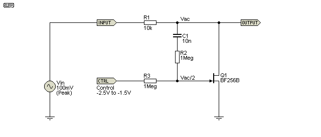
Figure 5 - JFET Variable Attenuator
The FET distortion is worst when there is a high voltage across the device, and can be made worse if the source impedance is low as this means higher current. This depends on the FET used - in the above circuit, distortion is actually worse if the value of R1 is increased. As shown, the maximum distortion is around 3.2%, when the peak output signal is at 80mV (56mV RMS). The control and output waveforms are shown below, but only the signal envelope can be seen because the time span is too great for a 1kHz signal to be visible. The control voltage varies from -2.5 to -1.5V across the span of the graph.
This general arrangement is used in countless audio peak limiters, but there is a hidden trap that is not immediately obvious. Imagine that the control voltage suddenly changes from -2V to -1V. The voltage at the gate of the FET will initially only change by 0.5V, because R2 and R3 form a voltage divider. With 10nF as shown, it takes over 80 milliseconds before C1 charges and allows the full 1V change (actually 990mV at 80ms) to reach the gate. This limits the basic circuit to relatively low attack times when used in a limiter, so many FET based commercial products use a more complex arrangement to ensure that the time constant does not cause problems. One solution to this problem is to make C1 much larger than necessary, so its influence is no longer relevant because the control voltage is always divided by two (or at least for long enough for the control circuit to correct for the change). C1 also couples a small control voltage signal through to the output, with the signal level depending on the circuit impedances.
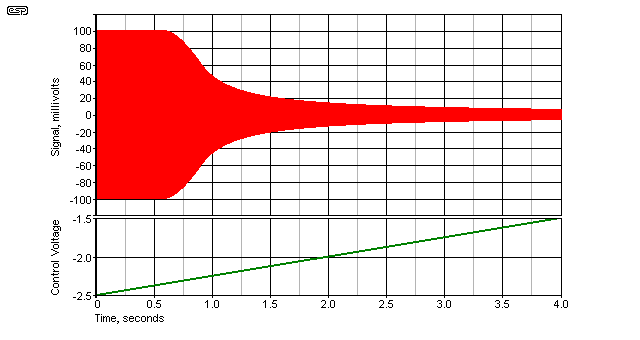
Figure 6 - JFET Variable Attenuator Waveforms
The red waveform is the signal envelope, and green is the control voltage. It's quite obvious that most of the control takes place over a rather limited control voltage range (between -2.35V and -2.1V). When the FET's gate is at 0V, the signal is reduced to 5.1mV peak, an attenuation of about 26dB. If the gate is made positive the FET will turn on a little harder, but the small amount of extra attenuation isn't worth the trouble (the attenuation is increased by a little under 9dB with +2.5V on the gate). The wider voltage swing is harder to accommodate with simple circuitry. It's also harder to ensure minimum control voltage feed-through (where part of the control voltage change appears on the signal line).
The distortion created by the FET is often very audible, so for low distortion compressors and peak limiters, the voltage across the FET must be kept to a minimum. This creates a conundrum though, because low signal voltages mean that more gain is needed after the gain control, increasing noise. There are many FET based limiters around (including one in the ESP projects page), and a few have achieved something akin to cult status amongst users. If the arrangement suits your needs, then there's no reason not to use it - compressor-limiters can be very personal choices.
It is not essential to use a negative control voltage. If the source is raised to around 3V above ground, the control voltage can then range from 0 to +1.5V and the result is identical to that shown above. However, there is now a DC voltage at the drain, so the input and output must be capacitively coupled.
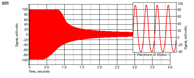
Figure 7 - JFET Attenuator Waveform Without 1/2 Voltage At Gate
For reference, the graph above shows the asymmetry created if the gate doesn't receive the 1/2 signal voltage. Where there is asymmetry, there is clearly a considerable amount of even-order distortion. The control voltage is identical to the example shown in Figure 6 and isn't repeated. The distortion reaches over 15% when the control voltage is -2.3V (850ms into the graph), just as the positive half cycles of the waveform start to be attenuated.
The inset shows a small part of the waveform. The distortion is clearly visible, with the positive peak at 92mV and the negative peak at 41mV. That is a completely unacceptable amount of distortion. It's primarily second order, and despite claims that this type of distortion sounds 'nice', it doesn't. Not even a little bit!
While you may imagine that a MOSFET could be used if the signal voltage is kept low, this is not the case. A MOSFET will create massive distortion, regardless of whether a 1/2 signal voltage is applied to the gate or not. Consequently, this option is not discussed.
The main things that you need to be aware of with MOSFETs is that they are primarily designed for switching, and that they have a very high gain compared to JFETs. They also have a comparatively high input capacitance, and this limits their frequency response with high impedance signal sources. Even small signal types (such as the 2N7000) have a gate-source capacitance of 20-50pF, which is around 10 times that of a 'typical' JFET. Where a JFET voltage amp stage might be perfectly happy with a 1MΩ source impedance, a similarly configured 2N7000 MOSFET will roll off the high frequencies from as low as 400Hz (-3dB).
The first MOSFET voltage amp shown below expects an input impedance of no more than 10k, and even then will have a -3dB frequency of less than 50kHz. As the source impedance increases, matters get worse. It can be helped by not bypassing the MOSFET's source resistor (R4 in Figure 8), which bootstraps the input capacitance and reduces its effect on frequency response. However, this will reduce gain and increase noise.
Because MOSFETs are designed for switching, they are not characterised for linearity or noise. The latter is important in low level circuits, and it's very difficult to find much real information on their noise performance. In general, I would expect them to be much noisier than JFETs and most BJTs, so using MOSFETs for amplifying very low signal levels is ill-advised, both for noise and input impedance.
Depletion mode MOSFETs are available, and these are 'on' with no gate voltage, in the same way as a JFET. A negative gate voltage is used to turn a depletion mode MOSFET off. However, these are relatively uncommon compared to enhancement mode devices, and consequently they are not covered in the descriptions that follow.
MOSFETs have much higher transconductance than JFETs, so more gain is available from a single stage. Because most common MOSFETs are enhancement mode, they need a positive voltage on the gate referred to the source to conduct. This means that a biasing scheme similar to that used for bipolar transistors is needed, and the inherently high impedance is not usually available because of the resistors needed for biasing and the input capacitance (which is a major limiting factor).
As with JFETs, MOSFETs have a fairly wide parameter spread, so biasing is again likely to be uncertain. As noted in the introduction, BJTs have the advantage that their base-emitter voltage is (comparatively) stable and predictable, but that does not apply to JFETs or MOSFETs. A MOSFET used as a voltage follower (source follower) is less of a problem, but voltage amp stages can be tricky to get right. For the most part, a JFET is a better choice for a voltage amp - especially if you need high input impedance.
In much the same way as a BJT is biased, a voltage divider is needed to set the gate voltage to that value necessary to maintain the MOSFET in its linear region. If it's saturated (turned fully on) or cut off (fully off) no gain is available. The gate potential is quite sensitive, because MOSFETs have a comparatively high transconductance, but an unpredictable gate-source voltage. This makes biasing without using feedback a somewhat tricky proposition. The use of a feedback biasing scheme ensures fairly stable operating conditions, but reduces the input impedance. A source resistor is also essential, as this provides another level of feedback. It can be bypassed so the feedback affects DC conditions but not AC gain.
Don't expect low distortion from a MOSFET voltage amplifier unless you add a current source in place of the drain resistor. Most MOSFETs are optimised for switching, and linearity is generally worse than JFETs, which in turn are usually worse than BJTs. This doesn't mean that you can't get good results, but it takes more effort. When you compare the results from any of the simple discrete devices to a decent opamp, there is simply no doubt that the opamp will outperform all of them other than for specific tasks (such as RF applications).
The same conventions as used for JFETs have been applied here. The gate-source voltage is +2.56V (note that it is positive, not negative as with JFETs). The input signal is 10mV peak, and the peak output is 2.33V - a voltage gain of 233 (47.3dB). However, the gain for the negative-going output signal is 240 - the difference is a clear indication of even order distortion, measured at 2.65%.
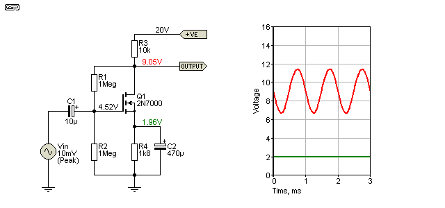
Figure 8 - MOSFET Voltage Amplifier
An unexpected result of using R1 joined to the drain is that it creates a negative feedback path. This reduces input impedance drastically. Rather than the 500k you might have expected, it's only 5k. The bias network can be connected as shown in Figure 8A, to remove the AC feedback. While the gain is impressive, distortion is over 2.6% - not so impressive. While the distortion is mainly (supposedly 'nice') 2nd harmonic, there's simply too much of it. If C2 is omitted, gain is reduced and input impedance becomes a more acceptable 300k.
There are a few things that can be done to make a MOSFET voltage amplifier somewhat more 'friendly'. However, it adds more parts than would be needed for an opamp doing the same job and still won't even come close in performance. No matter, as the next circuit shows what can be done to make the stage behave better. Because it has lower gain, the signal voltage has been increased to 1V peak (707mV RMS). There is no longer any AC feedback from the drain to the gate, so input impedance isn't compromised.
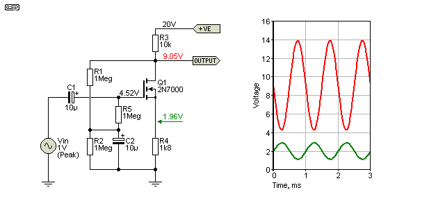
Figure 8A - Improved MOSFET Voltage Amplifier
The 'improved' version shown above has an input impedance of 1MΩ, but retains the DC negative feedback to stabilise the operating conditions. C2 removes the AC negative feedback. Because R4 is not bypassed, gain is reduced (and noise is increased), but it partially bootstraps the gate capacitance, and can provide passable frequency response with signal source impedances up to 100k (20kHz is less than 0.5dB down with a 100kΩ source). Gain is only 5.3 (14.5dB) and noise will be higher due to the noise contribution of R4, which is amplified by Q1 ... this always happens when a source or emitter resistor is not bypassed. Distortion is reduced greatly (to less than 0.1%, even at the much greater level), so it may be a worthwhile compromise.
To see how well (or otherwise) the simulation stacked up against reality, I built the Figure 8 circuit, but left R4 un-bypassed. DC conditions were quite close to the predicted values, and performance was acceptable. The circuit didn't add any audible noise to my workshop system, and distortion at 1V RMS output was below 0.1%. The -3dB frequency was over 400kHz when driven from a 50Ω signal generator - this is somewhat less than the simulation claims, but is still far more than necessary for audio.
It is possible to use a simple voltage divider to provide the bias, and that also avoids the feedback problem. However, it also means that the bias stability is poor because of the wide variation of gate-source voltage for different devices - even from the same batch. The datasheet says that the 2N7000 has a VGS threshold voltage for a 1mA drain current ranging from 0.8 to 3 volts. Most others are similar ... parameter spread strikes again.
In the same way (well, almost) as with a JFET, MOSFETs can be used as a mu-follower. The gain is a very impressive 6,4000 times (76dB), and output distortion with a 3V peak signal is 0.34%. However, there's a downside (but you knew that already  ). Input impedance falls dramatically, and for the circuit shown below it's only about 300 ohms. Meanwhile, output impedance is increased significantly to 200k - that's higher than many valve stages.
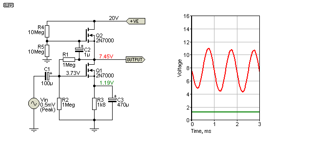
Figure 9 - MOSFET Mu-Follower Voltage Amplifier
Best you don't ask about frequency response. As shown, the response at the -3dB points is from 200Hz to 4.8kHz - telephone quality at best. Without feedback, the circuit has no practical value, and even with feedback its usefulness is doubtful. However, there may be a place for it in something, but I have no idea what that might be. Still, this article is about looking at the options.
A small signal MOSFET makes a rather good follower. Output impedance is low, and because of the relatively high transconductance the output voltage is not reduced as much as with a JFET. With 2V peak input, the output will be around 1.95V peak, and the output impedance of the circuit shown below is only 40 ohms, and distortion with no load is less than 0.001%.
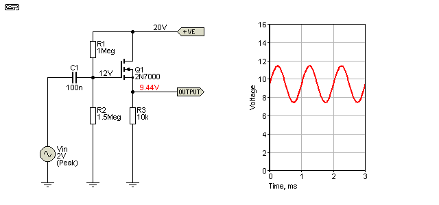
Figure 10 - MOSFET Source Follower
Unfortunately, the input impedance is much lower than for a JFET, because of the requirement for the two biasing resistors (R1 and R2). Input impedance is the parallel combination of the two, 600k as shown. This can be increased by using a bootstrap circuit (or a separate bias supply and feed resistor as used in Figure 8A), and an input impedance of over 50MΩ is possible, but high frequency response is poor with high impedance sources. If the gate is direct coupled to the preceding stage biasing is not required, and this makes it easy to provide low output impedance from JFET, MOSFET or valve (vacuum tube) voltage amplifier stages.
Use as a direct coupled follower is probably one of the best options, and although direct coupled BJT followers are common, the MOSFET is a better option where minimal loading of the previous stage is needed. You do need to allow for the voltage difference between gate and source, but for circuits operating with reasonable supply voltages (12V or more) it's easy to compensate for the ~2.5V offset that exists.
High voltage MOSFETs can be used to replace triode cathode followers in valve (vacuum tube) amps. They will provide a much lower output impedance, and outperform the cathode follower in all respects. Unlike a cathode follower though, there will be very little added distortion. The large gate capacitance is pretty much negated by the local feedback, so there will be no loss of high frequencies. There may be a small risk of damaging the gate's insulation if a protective zener diode (typically 12V) is not used between gate and source, but in most cases this is very unlikely. The MOSFET has an additional advantage of not needing any heater current (unlike a valve), and indefinite life.
In valve power stages, there is a lot to be said for using MOSFET followers to drive the output valves. This lets you use lower value grid resistors, ensuring much more stable operating conditions for the power valves, without excessive loading or loss of gain from the phase splitter. Few 'purists' will like the idea of course, even if it does improve performance and reliability. The IRF840 is a 500V MOSFET that is well suited to use as a follower in valve designs. There are also TO92 versions, such as the ZVN0545A or SSN1N45BTA, but their dissipation is limited to around 700mW. The STQ3N45K3-AP is rated for 3W and has internal zener protection for the gate, and at less than $1 no valve can come close. When TO92 MOSFETs are used like this, limit the current to no more than 2mA to keep the dissipation low (2mA at 200V is 400mW - adjust as needed for the voltage across the MOSFET).
You do need to be aware that the output of a MOSFET source follower will jump to the full supply voltage when used after a valve amplifier stage. This is because the valve does not conduct until the cathode warms up, and the sudden high voltage output may damage following stages unless protective measures are taken. Project 167 describes a suitable design, including protection circuitry.
MOSFETs can be used as signal switches, in a 'solid state relay' configuration. This works well, but there are a few things that have to be considered. The article MOSFET Solid State Relays covers most of the applications, but not signal level (100mV to ~10V RMS, low current) usage. There are two ways that a MOSFET 'solid state relay' can be used - either short the signal to ground or connect the signal through the relay. The latter does work, but the residual when the signal is off may be higher than expected, and distorted. With a 2V RMS source and a 2.2k load, expect an output of perhaps 2-4mV RMS, but very distorted (perhaps 10% THD or more as simulated - reality may be different). Consequently, the normally open (series) connection isn't recommended, with the preferred option being to short the signal to ground. However, this isn't without its limitations either.
One of the main issues (for both series or shunt operation) is that the gate supply should be floating. If it's not, you must use resistors to allow the gate to be biased, and that creates unwanted (and undesirable) interactions with the signal. Having a floating supply for each switch is a serious (and costly) nuisance to incorporate into the circuitry. There is a way around it though, which is to use a commercially available MOSFET relay that uses light activation. An example is the CPC1014 (made by IXYS) or similar. This not only has the switching function, but offers full isolation of the LED and switch, rated for 1,500V DC. There are many similar devices from other makers, but they may be more expensive than electro-mechanical relays and usually don't work as well. No matter, as they are interesting and useful.
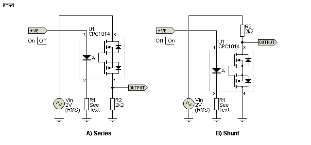
Figure 11 - MOSFET Relay (CPC1014 Example)
The series and shunt circuits are shown. In each case, a CPC1014 or similar is indicated. These are opto-isolated MOSFET relays, and are available from a variety of suppliers. They are available with voltage ratings from around 60V up to 250V or more, and all use a LED to turn on a pair of light-activated MOSFETs. By default, the gate-source region is completely isolated, so there's no need to mess around with a floating supply. It's certainly possible to make small signal (low current) MOSFET relays using discrete parts, but the end result will be far more costly than the IC.
The shunt connection will normally be the preferred option, because when used in series, the off signal may be rather badly distorted. It's a very low level (depending on the device itself), but the signal may still be audible and will not sound very nice at all. The shunt circuit's output level when on (signal shorted to ground) depends entirely on the on-resistance of the MOSFETs. The CPC1014 has an on-resistance of 2 ohms, so a 1V signal through a 2k2 resistor will be attenuated to less than 1mV (-60dBV). In reality the off level may be somewhat higher than 1mV, but it depends on the device characteristics. Note that the series circuit provides an output when the DC supply to the LED is on, and the shunt circuit provides an output when the LED is off.
You can operate these relays in a series/ shunt configuration, so when the series relay is off, the shunt relay is on. This shorts out any residual signal that may sneak through, and should be easily capable of providing more than 100dB of isolation. Obviously it's more expensive than a single switch, but it will work well. You'll probably find it hard to justify the cost compared to an electro-mechanical relay though, since a single DPDT relay can switch both stereo channels at once for less than $5.00 or so.
The LED current has to be kept below the rated maximum, and for most of these ICs, around 10mA is about right. The LED is infra-red, and these have a typical forward voltage between 1.2V and 1.4V. The details for the device you intend to use should be checked to make sure that all limits are observed. R1 is selected to provide enough LED current to ensure reliable operation, based on the datasheet suggestions and the available switched supply voltage.
As noted, the CPC1014 is only one of many similar devices. MOSFET relay ICs are made by many different companies, but the operating principles are identical. They are acceptably fast, with typical switching speeds being in the order of 3ms or less. Another option is the IR PVT422, which is a dual relay (two independent relays in a single 8-pin DIP package). On resistance is 35 ohms which is a limitation (but it's rated for ±400V). There is also the Omron G3VM-351, available in SMD and through-hole packages. However, it's on resistance is considerably higher than the CPC1014 because it's rated for a higher voltage. The Omron G3VM-21 types have an on resistance of only 40mΩ - a search will help you choose the right device for your needs. Note that these devices are very different from standard LED/ photo-transistor opto-couplers, and the standard types cannot be used in this role.
These devices are certainly interesting, and are definitely something that you should know about. In electronics, the most obvious choice is not always the most ideal. Most of the time, a conventional electro-mechanical relay is a better choice, but knowing that alternatives exist is always helpful. Prices range from less than AU$3.00 to AU$15 or so, depending on brand, type and package style.
One application where these devices would be very well suited is 'combo' guitar amplifiers. Standard relays can cause problems due to the vibration, but MOSFET relays are not affected. It's unlikely that too many commercial amps will use MOSFET relays due to the cost, but DIY amps are less of a problem because their builders are far more interested in getting everything right than saving a few dollars/ pounds/ euros etc.
The cascode topology is rarely (if ever) needed for audio, but it's common with RF, and was originally used with valves. This hasn't stopped people using cascode operation in audio of course, and in some specialised cases it may be worthwhile. The increased high frequency performance is due to the greatly reduced voltage swing at the output 'port' of the lower amplifier stage, so internal capacitance has less influence. If a voltage doesn't change (or only a little), the capacitance doesn't need to charge and discharge, so HF response is no longer affected. Essentially, a common emitter (or source) amplifier is direct coupled to a common base (or gate) amp stage, resulting in very high isolation from output to input, and much higher frequency response than can be obtained from a common emitter/ source amplifier. The primary reason to use a cascode circuit is when very high input impedance is needed, along with extended high frequency response.
Common gate amplifiers were not covered above because they are fairly uncommon as a stand-alone circuit. The upper FET (Q2) in the circuit below is operated in common gate mode, because the gate is connected to ground for AC. You may notice the similarity of the cascode circuit to the mu-follower. It appears (to me) that the mu-follower may have been a development from the cascode, but whether that was by accident or design is not known. Cascode circuits (with valves) date back to the 1930s.

Figure 12 - JFET Cascode Voltage Amplifier
The (simulated) -3dB upper frequency of the circuit shown is 154MHz, with a gain of 3.8 (11.6dB). The upper response can be extended further by using a small inductor in series with R5, which increases the load impedance at high frequencies. There is little or no need for cascode circuits in audio, but there are still people who insist that there are audible benefits. While I find this highly unlikely, as long as no-one claims 'magic' properties it's just harmless fun.
Cascode amplifiers can be made using any available amplifying device, and there's no reason not to mix two different types, such as a valve and MOSFET, JFET and BJT, etc. The biasing methods may change, but the basic idea isn't altered. Unless you are working with RF, it's unlikely that you'll need a cascode amp. There are countless examples on the Net if you want more ideas. Audio doesn't need response to several MHz, and it can also make interference from AM transmitters a great deal more difficult to suppress.
It's doubtful that this article has answered all questions, but hopefully it will set you off to find more information. There's a great deal of data and many circuits that you can play with, and you should now have an appreciation of some of the compromises that affect the designs you might come across. All circuits involve compromise, and there is no one amplifying device that is ideal for everything. We are spoiled for choice with opamps, BJTs, JFETs and MOSFETs, with the discrete devices available for either polarity, so spare a thought for the early designers who had a single choice - which valve to use for this or that application.
There is usually no good reason to use discrete parts instead of opamps in most audio circuits, despite claims that opamps somehow sound 'bad'. For some applications there may be no choice, especially when very high bandwidth is needed. I've (mainly) only shown the basic circuit arrangements here, but for RF work (in particular) the cascode circuit topology is very common because it provides a wide bandwidth and high input impedance with any given device (or combination thereof).
There are no recommendations, and note that the schematics are shown for reference - these are not construction projects, but are simply to demonstrate the different circuits available. All results and waveforms are based on simulations, but parameter spread means that real-life circuits will almost certainly need to be tweaked to get similar results. One point is very important though - the power supply has to be as clean (noise-free) as possible, because most of the circuits shown have very poor power supply rejection.
Failure to provide a clean supply will inject noise into the audio path, including hum, buzz and wide-band noise. A resistor/ capacitor filter following a 3-terminal regulator works very well, and I'd suggest somewhere between 10-100 ohms in series with the supply, with no less than 1,000µF (and preferably more) to ground. The 20V supply shown is simply a suggestion. Normally, anywhere between 15V and 30V will be alright, with higher voltages providing more leeway to account for parameter spread.
As already noted, the choice of JFETs is far more limited than used to be the case. Most of the very low noise types such as 2SK170 have gone. The LSK170 is an equivalent that is (allegedly) available, but I couldn't find it listed by any major distributor. Many others are still current, but often only in SMD versions. This makes them far less useful for DIY because of the tiny package and the requirement for considerable skill mounting tiny parts. A fairly large proportion of JFETs you can get easily (e.g. J105, 107, 109, etc.) are designed primarily for switching, so they are not optimised for linearity or noise. The BF256B (TO92) is at least a partial exception - it's an RF device but will still work fine at audio frequencies.
1 JFET and MOSFET Datasheets - BF256, 2N7000, 2SK170, etc.
2 CPC1014 and other MOSFET relay datasheets
3 Cascode - Wikipedia
4 Web search of 'mu-follower' schematics (many circuits found, not all are useful)
 Main Index
 Articles Index