
|
|
| Elliott Sound Products | Bootstrap |
 Main Index
Articles Index Main Index
Articles Index
|
It's unclear when (or by whom) the term 'bootstrap' originated, but a web search will (as always) provide numerous answers, most of which are likely to be wrong. It's often described as the rather unlikely situation where a person lifts him/herself off the ground by pulling on his/her bootstraps (a loop at the back of boots to help pull them on). This is not a scientific description by any means, but it does paint an amusing mental picture. 
Bootstrap circuits are often misunderstood, partly because they are a bit weird, and partly because there are several different types with very different functions. They are unique to electronic circuits, and while it may be possible to create a mechanical bootstrap 'machine', I can't think of a use for it. There is some mention on the Net about a 'bootstrap' system for air-conditioning systems used in aviation, but that's not relevant here.
'Bootstrap' also refers to an open-source web development framework [ 1 ]. It's intended to make the web development process of 'mobile-first' websites easier, by providing a collection of syntax for template designs. It (apparently) helps web developers build websites faster as they don't need to worry about basic commands and functions. It consists of HTML, CSS, and JS-based scripts. This article does not cover this.
In the field of electronics, bootstrap circuits are used to increase input impedance, create 'constant current' sources (particularly [but not restricted to] audio power amplifiers), and to provide a voltage above the main supply rail (Class-D amplifiers, switchmode PSU controllers). A bootstrap system can also be used to allow an opamp to function over a wider than normal supply voltage range, effectively eliminate input protection diode capacitance, or even to make the capacitance of a cable 'disappear'. Unfortunately, the same term is used for all (bootstrap) and it can be difficult to know which is which unless you understand how each one works.
There's even a form of bootstrap circuit used for PCB design, to prevent leakage across the board from upsetting high-impedance circuits. In this mode, it's called 'guarding', and uses a small length of PCB track to encircle a high impedance point. The guard is hooked up to a low-impedance point with the same potential as the input. This is the one application of bootstrapping circuits where it can be used for DC. The guard ring prevents leakage currents from upsetting the circuit's operation, but it doesn't change the input impedance. It's arguable if this really qualifies, but it is a form of bootstrapping IMO.
There are many examples of bootstrap circuits on the ESP website, especially for creating 'constant current' to linearise an amplifier. One thing that's a bit limiting is that all common bootstrap circuits only work with AC. DC operation is not possible because the bootstrap device is a capacitor. Always. If you need a constant current source that works to DC then it must be active (i.e. using an IC, transistor, JFET, etc.). For linear AC, adding bootstrapping usually involves the addition of one resistor and one capacitor. With switchmode converters you add a diode and a capacitor.
There is information on the Net covering bootstrap circuits, but a great deal of it is overly simplistic, explained poorly, or just wrong. Some is seriously wrong, despite lengthy descriptions and scope displays. I don't link to material that's not accurate. There's also a fair bit of other information that's correct, although in some cases it's highly specific to a particular application. In some cases, it looks like authors have made assumptions, but never verified that what they describe is real. This isn't helpful to anyone.
To understand the two most basic (and earliest) forms of bootstrapping, we don't have to delve into complex maths or anything else that's 'challenging'. A simple mental exercise is pretty much all that's required. This can be augmented with a simulation or a bench test (if you have the necessary equipment). At it's heart, bootstrapping ensures that the AC voltage appearing across a resistor remains constant. If the voltage across a resistor doesn't change, then the current through it doesn't change either.
This applies whether the circuit is configured for boosting the input impedance or providing a constant current. The two are fundamentally equal in all respects. The goal is to make a resistor appear to have a value that's many times its actual value. As shown below, we can make a 5k resistor behave as if it were over 100MΩ, by ensuring that the AC voltage across the resistor is constant. As noted above, if the voltage across a resistor is constant, then the current through the resistor must also be constant. Ohm's law shows this to be true.
In the examples shown, the voltage source can swing below ground, as would be the case with a transistor (for example) with both positive and negative supply voltages. We need only consider positive transitions for basic analysis. The only part of this that may be a bit confronting is that the impedance (apparent resistance) is different for AC and DC. However, inductors and capacitors are similar, in that AC and DC conditions are very different.
Bootstrapping is an AC process, and while it can (in some cases) be adapted for DC, there are other topologies that achieve a result that's superior and easier to implement. Consequently, only AC applications are considered throughout this article and in (most of) the examples that follow. The two primary applications are increasing the input impedance of a circuit, or providing a constant current to obtain higher gain and linearity from an amplifying device. These are explained in detail below. These two processes are essentially identical, as both rely on making a resistor appear to have a much greater value than its physical resistance (technically, this is impedance, not resistance). In the drawing I've shown a simple voltage generator, but in practice it will be a transistor (BJT, JFET or MOSFET) or even a valve (vacuum tube). The principles are unchanged, but the effect can never be as good in reality as it can with 'perfect' parts.
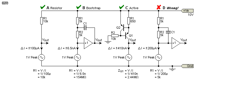
With an ideal current source, only the voltage changes, but the current remains the same. Predictably, the 'ideal' doesn't exist, but we can get fairly close. In the drawing ('A'), a voltage source is shown, with a resistor supplying the DC current needed for operation. This can range from nA to mA in 'typical' circuitry, but in this case it's 1mA. If the source voltage varies by ±1V, the current through the source must vary by ±100µA (Ohm's law). If the voltage is increased to 5V peak, the current varies from 0.5mA to 1.5mA. A calculation will result in an answer of 10k at any voltage.
In the second circuit ('B'), a buffer is used to isolate the source (the buffer cannot be left out!). C1 couples the output of the buffer to the junction of R1 and R2. This forces the voltage across R2 to remain constant. In all cases, Vout is assumed to be a high impedance (1TΩ was used for the simulations - that's the input impedance of a TL07x JFET opamp). The buffer stage can be an opamp, a BJT emitter follower or even a MOSFET source follower. The gain is expected to be unity, but it will never be exactly 1 - somewhere between 0.999 and 0.98 is generally normal. It must be less than unity - if it exceeds unity you'll be applying regeneration (positive feedback) that boosts the gain, and it may oscillate.
Ohm's law lets us determine the effective resistance (impedance) for each condition shown. The AC values shown are peak. Predictably, the resistor in 'A' can be calculated to be 10k. In 'B', R1 is bootstrapped, and with a unity gain buffer (and allowing for the impedance/ reactance of C1), the effective value of R2 becomes 154MΩ. The current through the source varies by only ±6.5nA (ΔI means change of current). If all parts were 'perfect' (and assuming C1 to be infinitely large), the effective value of R2 becomes 'infinite'. This does not (and cannot) apply to any real circuit.
Circuit 'C' shows an active current source, configured for (close to) 1mA DC as with the others. The output impedance measured at the collector of Q1 is 2.44MΩ (close enough). A bootstrap circuit using real parts can be slightly better, but the difference is usually negligible. However, the active version does something that a bootstrap circuit cannot - it works to DC. This is important for some applications, but not for others.
You may initially wonder why the buffer is so critical, so consider condition 'D' (perhaps that should have been 'F' for 'fail). I (almost) never show something that's so obviously wrong, but it's a circuit you'll see on many websites and it's claimed to be 'bootstrapped' (it's not). It doesn't work, it can't work, and even the most rudimentary analysis proves this to be true. The capacitor simply shorts R2 for AC, at a frequency determined by R2 and C1. The source 'sees' 10k for DC and 5k for AC at some frequency. This is the opposite of bootstrapping! Although I generally avoid showing things that don't do what the 'author' claims, this had to be included because it's repeated so often, and it requires debunking!
Remember that bullshit is still bullshit regardless of the number of times it's repeated. Mindless copying on the Net is the source of more dis/mis-information than most mortals can handle.
The bootstrap process is possibly best known in a mode where it boosts input impedance. This can be very useful, because it's possible to get very high Z-in (input impedance) even with low-value resistors. Normally, the input impedance of an amplifier stage is determined primarily by the biasing resistor(s), but if high values are used this will increase noise. Any resistor at a temperature of greater than 0K (-273°C) makes noise, as covered in the article Noise In Audio Amplifiers. This can be reduced by using lower values, and applying bootstrapping to obtain the desired input impedance.
One thing to be aware of ... bootstrapping involves positive feedback. Most people know that negative feedback improves the bandwidth of an amplifier and reduces distortion. Positive feedback can do the opposite. There may be a small increase in distortion (only for input bootstrapping), and the bandwidth may be reduced. Neither is guaranteed though, as it depends on the overall topology of the circuit. It will never normally be a problem.
The general idea is described in detail in the article/ project High Impedance Input Stages / Project 161, and that covers the bootstrap circuit in great detail. This is a very common application, and it can work very well. A small miscalculation can have unexpected ramifications though, so a full understanding is essential. When used to boost input impedance, positive feedback is involved, and that can lead to instability. The gain of a bootstrapped input stage must be less than unity. A JFET follower will typically have a gain of ~0.9, a BJT follower will be around 0.98, and an opamp buffer has a gain of 0.999... The gain of an opamp buffer is highest (closest to unity) at low frequencies, and it falls ever so slightly with increasing frequency (within the device's bandwidth).
Common circuits such as valve cathode followers or JFET source followers may end up with a bootstrapped input without you realising it. Two circuits are shown next, and both feature bootstrapped input resistors (R1 in each circuit). Most people will assume the input impedance is 1MΩ, but it's not. The 'lower' end of R1 in each case isn't at 0V AC, but is at an AC voltage of about VIn / 1.1 (i.e. about 0.9V for a 1V input).

The two circuits shown are more-or-less equivalent (inasmuch as a valve and FET can ever be), and both have an 'accidental' or perhaps 'incidental' bootstrapped input. They were simulated, and I made no real attempt to optimise either circuit. If the cathode/ source resistor (R2) is bypassed with a capacitor (C3, optional), the effect is improved somewhat. Without bypassing, the input impedances are 25MΩ (12AX7) and 5.9MΩ (JFET). The valve circuit benefits the most from a cathode bypass, with the input impedance increased to 54MΩ. There's a more modest increase with the 2N4584, to 22MΩ. The input impedance falls at high frequencies because the grid/ gate capacitance becomes dominant.
These aren't usually thought of as being bootstrapped, but they are whether you want it or not. There is no form of unwanted interaction - the input resistor is simply buffered by the cathode/ source. The application of 'bootstrapping' occurs whenever you have a buffered version of the input signal applied to the 'other end' of the input resistor. In an ideal case, the voltage at both ends of R1 would be equal, meaning that there can be no current, and the resistor no longer exists (for AC) as seen by the source. It still passes DC bias current though.
Everything changes when you use an opamp, because when configured as a unity gain buffer, the output level is almost identical to the input. With valves, JFETs or transistors this is not the case (their gain is always slightly less than unity). Provided there are no added filter poles, simple bootstrap circuits as shown in Fig. 2.1 are completely benign, despite the use of positive feedback.
Unlike positive feedback that may be used to boost gain (as was common in very early 'regenerative' radio ['wireless'] receivers), the positive feedback doesn't increase the gain or become unstable at high frequencies. Instead, it causes low-frequency problems, where the circuit may end up functioning a little like a high-pass filter (of obscure lineage). This is explained in detail in the referenced ESP article, but is generally not discussed elsewhere. The 'filter' action can create low-frequency boost, and it's important to ensure that it doesn't cause problems within the frequency range of interest.
The bootstrap circuit can be added to a follower or a gain stage. Both are shown below, and the relative responses are almost identical. The gain stage simply elevates everything by 20dB, since it's configured with 20dB of gain. The added bootstrap components (R2, R3 and C2) increase the gain very slightly (0.06dB) as the network is effectively in parallel with R6 (200Ω).
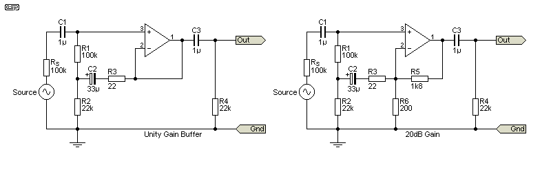
The circuits shown above have an input impedance of more than 10MΩ from 20Hz to just under 20kHz, and the upper frequency can be raised by using a faster opamp. The 1µF cap (C3) is deliberately selected to roll off frequencies below 7Hz to reduce the amplitude of the low-frequency peak. Without that, there's a peak of 3dB at 0.7Hz, caused by the interaction of the source impedance (100k), and the value of C1 and C2. These form a complex relationship, with R1, R2 and R3 forming a peaking filter. If the source impedance is changed, so too is the peak frequency, but fortunately not by a great deal - provided it remains high. If the source impedance is reduced to (say) 10k, the peak increases to 7dB! There's an impedance dip at the 'resonant' frequency, and with the circuits shown it falls to 124kΩ at 0.7Hz.
R3 is included to suppress the peak, and it's only ever needed when you bootstrap an opamp. It's 'implied' with a BJT (bipolar junction transistor) or JFET (junction Field effect transistor), because they have a gain that's less than unity. The Fig. 2.2 circuit still works without R3, and the input impedance is increased a little - except at the peak frequency of 0.7Hz. The amplitude of the peak is greater without R3, as you'd expect.
One thing you discover quite quickly is that simulations and 'real life' can be quite different. The circuit of Fig. 2.2 (Unity Gain) may simulate perfectly, but in my opamp test board (using NE5532 opamps), there is noticeable rolloff at high frequencies when the source is 1MΩ. A -3dB frequency of 25kHz isn't much good for audio, but very few signal sources have such a high impedance, so it's usually not going to cause any problems. The rolloff is caused by stray capacitance and the input impedance of the opamp. It's generally better to use a high input impedance opamp (e.g. TL072, OPA2134, etc.) if you need to cater for high impedance sources.
With the Fig. 2.2 circuits, you could be excused for thinking that the rolloff (before C3) would only be 6dB/octave, since it's controlled by the value of C1 and the effective value of R1 (say 10MΩ). However, the rolloff below the cutoff frequency is 12dB/octave (second-order) because of C2. Knowing this tells us that we have created a filter, accidentally or otherwise. The response eventually levels out to 6dB/octave, but only at unrealistically low frequencies (~100mHz or 0.1Hz). You may find this discussed in books covering analogue electronics, but it's usually never mentioned. As a result, a bootstrap circuit that uses (what appear to be) sensible component values (e.g. 10nF for C1 and 10µF for C2) causes low-frequency boost that may be most unwelcome. With the combination of 10nF and 10µF, there would be a peak of 20dB at ~6Hz. This can be mitigated to a degree by including the high-pass filter at the output.
Understanding the implications of each value is important, otherwise you can face problems, and not know why it's happening. Since we now know that we've created a filter, it should also be apparent that like all filter circuits, the source impedance will affect its performance. The filter may not be a common type (e.g. Sallen-Key, Multiple Feedback, Fliege, etc.), but it most certainly is a filter, and as such should be designed for the expected source impedance. If the source is capacitive, that complicates the process. Most capacitive sensors need a high impedance preamplifier, but the total capacitance has to be used for the design - this includes the capacitance of the cable.
When a capacitive sensor is used (typically a piezoelectric device), its output is reduced by cable capacitance. A 1nf sensor with a 1nF shielded cable (perhaps 5 metres of cable at 200pF/ metre), the output level will be half that expected. The piezo/ cable circuit is a capacitive voltage divider, which works in the same way as a resistive divider. In this case, the capacitive load 'seen' by the input bootstrap circuit is 2nF, as the two are effectively in parallel. You can design for flat response with this arrangement, but if the sensor or cable is changed, the circuit has to be changed to suit.

The graphs were made using the circuits in Fig. 2.2, and only C1 was altered. It makes very little difference if the circuit has gain or not, as the effect is almost identical. Four response curves are shown, using four different values for C1. As the value is made larger, the peak moves to a lower frequency and becomes better damped. If R3 (22Ω) is omitted, the 6Hz peak is increased by about 1.5dB, with less effect with higher capacitance. Once the input cap is large enough, there is no peak, as shown for 10µF. Of these, 1µF is the optimum choice, but only for a 100k source impedance. If that changes, so does everything else. The response shown is without the final high-pass filter (C3, R4).
All amplifying devices can use a bootstrapped input. It works with valves (vacuum tubes), BJTs, JFETs, MOSFETs and opamps. With any device that doesn't have almost perfect unity gain (i.e. anything that's not an opamp), the input impedance isn't increased as much, and the chance of a high-Q bandpass filter (the red trace for example) is minimised. R3 tames the peak to some extent, but it also reduces the effective input impedance.
The theory behind this is quite simple. C2 passes the buffered input signal to the junction of R1 and R2. R2 is only present to ensure there's a DC path to ground so the opamp will function. The voltage across R1 does not vary with the input signal because of C3, and if the same (AC) voltage appears at both ends of a resistor, there can be no current flow. If no signal current can flow through R1, then it must have a very high value (many, many, times the actual value. In this case, it becomes equivalent to at least 10MΩ, despite being only 22k. The bandpass filter is created by complex phase relationships, and I'm not going to try to analyse it because it's an unwanted complication. You only need to be aware of it so that your design isn't compromised.
I've left the simple emitter-follower circuit until last, because it's the least useful. This is due to the requirement for base current to bias the transistor. The input impedance of a transistor emitter follower circuit is far lower than that of a valve, JFET or opamp. The base requires current, and that has to be provided by the biasing circuitry and the signal source. The input impedance is also directly related to the output impedance. This includes the emitter resistor and the external load.
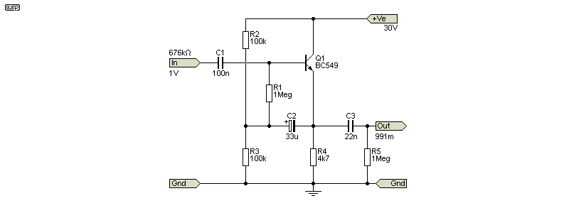
The simple circuit shown above has an input impedance of about 620k without C2, due largely to the input impedance of Q1 itself. The impedance at the base of Q1 is roughly equal to the load impedance (4.7k) multiplied by the hFFE of Q1, in this case about 350 (200 to 800 is 'typical' for a BC549). We have ~1.6MΩ for Q1 and 1MΩ for R1, and as they are in parallel, the result is ~620k. If R1 is bootstrapped with C2, the effective resistance of R1 is very high (> 100MΩ above 10Hz), but the transistor's input impedance is dominant. As there's also a small additional load on the emitter circuit, the transistor's input impedance is reduced a bit. The simulator tells me that ZIN is about 1.4MΩ for the circuit shown.
While bootstrapping certainly works with BJTs, it's not possible to get extremely high input impedances with a simple circuit. This limits the usefulness of the technique unless you're willing to add a more complex circuitry. A Darlington transistor can increase ZIN to over 10MΩ, but it's still not ideal. If you need ultra-high ZIN, then an opamp or a discrete JFET will almost always be a better proposition. This will be most of the time, since valves are very expensive (and may have limited availability), but suitable JFETs can be found (they are rapidly becoming difficult to find though).
The same circuit as Fig. 2.4 can be used with a small-signal MOSFET (e.g. 2N7000). While it will definitely work, MOSFETs are fairly noisy, so it's not a good solution for low-level signals. Because of the high transconductance of MOSFETs (at least when compared to JFETs), a resistor will almost certainly be needed in series with C2 to prevent peaking (as occurs with an opamp). If you simply substitute a 2N7000 for the BC549, use a 2.2k - 10k resistor which will minimise problems within the audio band. A higher resistance means a lower input impedance.
One thing to be aware of is the frequency dependence of the bootstrapped input. All circuits will show a reduction of input impedance as the frequency gets above (about) 5kHz or so (it depends on the device and the bootstrap component values). This may or may not be a problem, depending on the application. It's worth noting that most instrumentation systems that require a high input impedance use a high-value resistor (e.g. 1GΩ or more), and do not use bootstrapping. Frequency response issues and variable input impedance are unwanted effects for measuring instruments.
In Project 13, I showed a simple 2-transistor circuit that is quite extraordinary, despite its simplicity. It uses a bootstrapped current source (R2). The bootstrap capacitor (C2) ensures that the same voltage is present at both ends of R2, and logically, if the voltage across a resistor is constant, so too is the current through it. The nominal current through R2 is ~160µA, and with C2 it varies by only 74nA. With the values shown, the voltage across R2 is about 6.3V DC, but only 1.5mV AC (with a 1V output). The effective impedance of R2 can be as high as 10MΩ, simply due to the bootstrap capacitor. The result of this is that the gain of Q1 is increased by several orders of magnitude, and because the current barely changes, the linearity is much greater than you'd expect from a simple transistor stage. The effective resistance of R2 is greater than 4MΩ at 10Hz, rising to 12MΩ above 100Hz.
Without C2, the open-loop gain ('RG' open circuit) was simulated to be about ×260. When C2 is connected, the gain increases to over 600. Not only is the gain more than doubled, but distortion is reduced by ×1.5. That really is a win-win - more gain and lower distortion, with the addition of one resistor and one capacitor. At maximum output, the voltage at the junction of R2, R3 and C2 can exceed the supply voltage - this is true bootstrapping!
An active version is shown next. In theory, this should be 'better', but the difference is academic. There will always be differences between the two, but the differences between the transistor parameters used in any two 'equivalent' circuits will usually be far greater than any difference due to the topology. The results shown here have all been simulated, and simulators have identical transistors of a given type, and exact value resistors.

An active CCS (constant current source) is shown above for reference. Both bench tests and simulations show the two different versions to be virtually identical. There are differences of course, but nothing that will be audible, and even measurements may not reveal any change. There is a small difference due to the active CCS having slightly lower current and a higher impedance at low frequencies. This small advantage is only true up to ~2.5kHz as simulated. Real life will be very similar. Component parameter spread will cause greater differences than anything else.
One circuit that's quite common on the Net is supposed to be a linear 'time-base' sweep circuit. It uses bootstrapping to create a current source that charges a capacitor for a linear sweep. Whoever published it first neglected to point out its many failings, which make it pretty much useless (well ok, it's utterly useless). Predictably, it's not shown here because there is no point. It could improved quite easily, but I don't expect that it would be of much interest. If you're building a time base, you won't be cutting corners with sub-optimal circuitry that's been fudged to provide a not-quite-barely-acceptable result. I have no idea how/ why such flawed ideas get so much coverage on the interwebs.
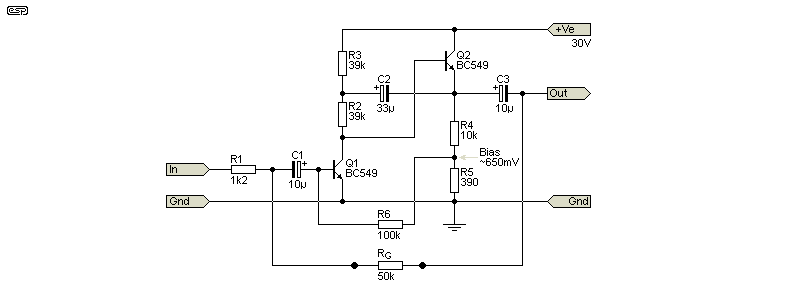
The same bootstrap arrangement seen in Fig. 3.1 is used for power amplifiers, and it's used in P12A (El Cheapo), P3A, P68, P101, P127 (The TDA7293 IC uses a bootstrap circuit internally), and P217 (low power 'practice' amp). In short, nearly all ESP power amp circuits. In these roles, the bootstrap circuit works in exactly the same way as described above, except the resistor values are lower because the Class-A amplifier stage (aka VAS - voltage amplifier stage) needs more current. The measured difference between an active current source and a bootstrapped current source is generally tiny (assuming an optimised design).
Using bootstrapping seems to have fallen from favour with most designers, and I don't know why. There's no doubt that an active constant current source works very well, but so does bootstrapping. There are (slightly) fewer parts, and the average current through the VAS will vary slightly as the supply voltage changes, but that usually makes little to no difference to the amp's operation (and it often happens with both methods anyway). Certainly, no-one has ever complained about the sound quality of any of my designs. Some early single supply amps made cunning use of the output coupling capacitor to provide bootstrapping - an example is Project 12.
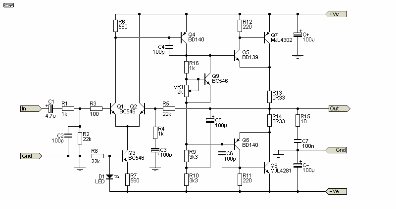
The bootstrap circuit uses R9, R10 and C5, forcing the voltage across R9 to be essentially constant. As already noted, if the voltage across a resistor is constant, so too is the current through it. Just like the previous example, the gain of Q4 is boosted due to the high impedance load, and linearity is greatly improved. An active current source makes surprisingly little difference to the gain or linearity of the VAS transistor (Q4), but there is a marginal increase in circuit complexity. I doubt that the performance difference would be audible (even tiny differences can be measured), but an extra active device (a current source transistor) might affect high-frequency stability. The transistor will always have a finite frequency limit, where the bootstrap circuit will work at almost any frequency. The only 'trap' is to make the value of C5 too low to ensure good linearity at the lowest frequency of interest (typically 20Hz, but most amps are expected to operate down to lower frequencies).
The effective impedance of R9 is around 170k. That's an increase of more than ×50, without upsetting the DC operating conditions. With the 100µF cap (C5), the effective impedance is greater than 50k at 10Hz, and is >100k at 20Hz. For an electrolytic capacitor in this role the ESR (equivalent series resistance) is irrelevant, as it's too low to cause a problem. The cap will generally last for 20 years or more, as the ripple current is very low. I don't recall ever having to replace a bootstrap capacitor.
For anyone who accepts the bogeyman stories about how 'bad' capacitors are, then the bootstrap circuit can't possibly be any good. More rational people understand that capacitors are perfectly fine when used appropriately, and there's no reason to lose sleep just because there's one extra cap in a circuit. I don't subscribe to these silly claims, as regular readers will know.
The bootstrap circuit can be replaced by an active current source as shown in Fig 2.2, but reversed polarity (it's referenced to the negative supply). That will add one or two transistors, two resistors, and perhaps a couple of diodes. The performance difference is generally small, so the bootstrap circuit wins for component count and overall cost. It's also an opportunity to use a very clever circuit. Despite the constant current supply to the VAS, its current still varies because it has to provide current into the driver and power transistors. This happens regardless of the type of current source - active or bootstrapped.
There is a limit though, and bootstrapping only works with AC. If you like listening to DC, then use an active current source. This will affect a very small number of listeners.

The 'amplification factor', (aka mu or µ) for a 12AX7 is generally taken to be 100. This is the maximum gain you can get from the valve, and it is rarely achieved in practice as it requires an impossibly high plate resistance. However, if the plate resistor (R3) is bootstrapped as shown above, it becomes (effectively) much higher than its physical value (over 4MΩ as simulated). The circuit has a gain of 39dB, just 1dB shy of the maximum (40dB). The distortion is also reduced dramatically, and with a 10V peak output (7V RMS) it's only 0.16%. This is a circuit that I've built and tested, although I used a 12AY7 in my original circuit, originally developed over 40 years ago.
Without bootstrapping (R2, R3 replaced with a single 200k resistor), the gain is reduced to 36dB, and distortion rises to 0.48% with only 4.7V RMS output. Predictably, the distortion falls with reduced level. The stage has enough gain to allow the application of feedback to get a reduced gain with even lower distortion. With a gain of 20dB (×10), the distortion is 0.0036% with 1.4V RMS output. This is almost unheard of for a valve stage.
You're unlikely to see this often. The technique (as near as I can tell) was first published in August 1947 in Wireless World (British publication), and was applied to a pentode. The general idea was published on the ESP site in 2009 (see Valve (Vacuum Tube) Preamps, but it existed on my site well before that. I constructed my first prototype in around 1980, independently of the original design (which I had not seen at the time). While it remains an interesting circuit that works very well, it's no longer viable due to the cost and comparatively poor performance of valves you can get today (and they are inordinately expensive).
Many people will have seen this final version of bootstrapping, but were unable to work out what it does. This is no surprise, as explanations in datasheets are generally lacking. You'll find info on the capacitor size needed and the requirements for any external diode (some are internal to the IC), but not much on how it works. This arrangement is most common in Class-D amplifiers, where the cap is indicated as 'CBOOT' or similar. You can probably work out how it functions if you read the datasheet thoroughly, but some are many, many, pages long, with bits of info scattered throughout.
It's debatable if this is a 'real' bootstrap circuit or a simplified charge-pump, but that's immaterial if you want to know how it works. A simplified diagram is shown next, with the essential parts being the output switching MOSFETs, CBOOT, DBOOT and VCC (a 12V supply rail). VDC (the input voltage that's switched by the MOSFETs) can be anywhere from 50V to 200V, sometimes more. Around 400V DC is common for a high-power SMPS (switchmode power supply) that operates from rectified mains voltage.
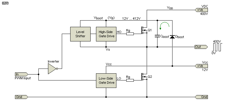
Unlike the previous forms of bootstrapping that worked continuously in the time domain ('pure' analogue), this type is periodic. CBOOT is charged only when Q2 turns on, pulling the output low or to ground. Current flows from VCC to CBOOT via DBOOT - the bootstrap diode. When Q2 turns off, Q1 turns on, and the gate driver uses the charge stored in CBOOT to provide the voltage and instantaneous current demanded by the MOSFET's gate. Without this bootstrap circuit, it would be necessary to provide an additional floating power supply to enable the gate voltage to exceed VDC, typically by 12V or so. This process is repeated at the switching rate, and can be anywhere from 50kHz to 500kHz.
I've kept the circuit as simple as possible to eliminate any confusion. The PWM (pulse-width modulated) input drives Q2 directly, via the 'low-side' gate driver. The 'high-side' consists of a level-shifter and the high-side gate drive. Both of these are supplied by Vboot, which will be 12V greater than the incoming DC (400V in this example). When Q2 turns on, the output is close to ground, so current flows from VCC (12V), through Dboot and charges Cboot to 12V. When Q2 turns off, the inverted input signal provides gate voltage to Q1 via the level shifter, using the 12V stored on Cboot, referred to the output. The current path when Q2 is turned on is shown by the green arrow.
Vboot is not a steady DC voltage - it varies from 12V (Q2 on) to 412V (Q1 on). There is additional circuitry (not shown) that prevents Q1 and Q2 from turning on at the same time (that would short-circuit the 400V supply). Every time Q2 turns on, the charge in Cboot is replenished. Without the extra voltage, Q1 would be unable to turn on at all, as there's no gate voltage available. The points marked as 'HO' and 'LO' simply mean 'high out' and 'low out' (gate drive signals).
Higher frequencies require less capacitance, but a faster diode. The bootstrap diode will always be a fast switching type - standard diodes (e.g. 1N4004 etc.) are too slow, and cannot turn off quickly. This arrangement is ubiquitous in switching supplies and Class-D amplifiers. There are quite a few circuits where the bootstrap system relies on some additional internal circuitry, and it's not always clear that it is bootstrapped.
Note that I haven't tried to explain the start-up process. Q2 must turn on first, otherwise there is no opportunity for Cboot to obtain a charge. ICs using this scheme are very common, and can be found in countless push-pull switching circuits. There are complete ICs that include signal conditioning, level-shifters, bootstrap connections and everything needed to switch a pair of MOSFETs.
It may seem like there's at least a bit of 'black magic' involved, but it's actually quite straightforward once you understand the concept. There are similarities between this and the power amplifier bootstrapping described above, but the difference is that the audio circuit has to operate over a wide range of output voltages (it's analogue audio), whereas for an SMPS the output is either 'high' or 'low' - 400V or zero for this example. The 400V supply can be replaced with any other (positive) voltage - even as low as 12V!
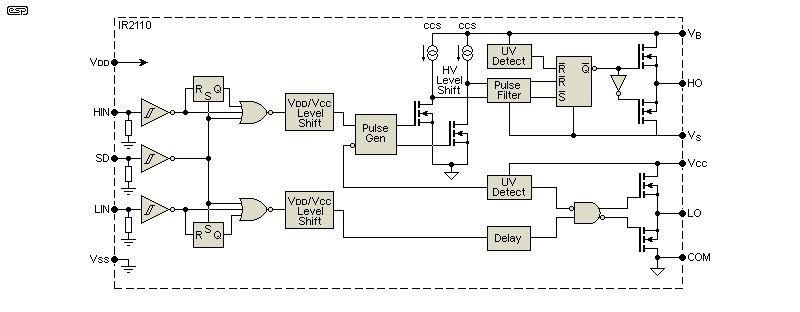
For this to make complete sense, it's useful to examine a typical MOSFET gate driver IC, in this case the IR2110/ 2113. The high-voltage supply is not connected to the IC. The 'VDD' pin is the logic supply for the IC. 'VB' is the bootstrap voltage. The entire high-voltage section (everything after the 'HV Level Shifter') has its reference voltage (Vs) switching between from 0V (GND) and +400V for this example. The level shifter is really the heart of the circuit, and it's another clever circuit (but outside the scope of this article). The upper MOSFET driver circuits (UV [under-voltage] Detect, Pulse Filter and other logic) have the supply voltage (VB) switching from 12V to 412V.

Another class of IC that can use bootstrapping is called a charge-pump. These often use a system that's very similar to that shown for the SMPS controller/ IRS2110, etc. There is only one voltage applied, and the charge-pump boosts the input voltage by two. This allows you to get a +10V supply when the only voltage available is +5V (or ~24V from 12V). An example is the Microchip TC7660, with the only real difference between that and the conceptual circuit being that it uses a synchronous rectifier (aka 'ideal diode') to improve efficiency. These are not high-current devices, and are generally limited to around 200mA or so maximum, with <50mA being more typical. There are variations designed to generate a negative voltage, and they're available from all the major IC manufacturers.
Q1 gets the high gate voltage needed (+24V) so it can turn on, and some of the charge on Cboot is passed to Cout each time the output switches high (Q1 on). One of the main reasons that the bootstrap circuits are so common is that N-Channel MOSFETs are more readily available and have better performance than P-Channel devices. The small extra effort of adding the bootstrap means that the entire IC can be built using N-Channel MOSFETs. While the circuit shown in Fig. 4.3 is conceptual (it has been simulated), if you were to build it, it would work as expected (use 2N7000 MOSFETs). The switching frequency will typically be at least 100kHz. The output voltage can be expected to be about 22-23V (perfect doubling isn't possible due to diode and MOSFET losses).
Like any switching circuit, a charge-pump generates EMI (electromagnetic interference), and there is no regulation. As you approach the maximum allowable output current, there may be substantial ripple superimposed on the DC. With the version shown (and a 100kHz oscillator) the ripple is 12mV p-p (about 3.5mV RMS) at 20mA output. This can be reduced with extra filtering, but then you lose the main advantages (low cost and small PCB real estate).
Most explanations of charge-pump circuits show a number of switches, that are used to a) charge the bootstrap cap, and b) connect it in series with the supply. These are quite valid, but they don't explain how the circuit actually works. Long before charge-pumps, there was the Cockroft-Walton voltage multiplier - if you don't know about it, look it up. Generally using multiple stages, these can generate very high voltages (kilovolts), but at low current. This isn't particularly relevant here, but it shows that voltage multiplication is not new.
Bootstrapping is one of those things that doesn't appear to make sense until you look into exactly how each version works. The techniques have been used for many years, and the term 'bootstrap' has even been applied to computer software (e.g. 'bootstrap loader'). The latter is a small piece of code that is executed when a PC or similar is powered on, and it loads the operating system. This technique is no longer used in most cases.
I've not been able to determine when bootstrapping was first used or in what form. No early valve equipment that I've come across used it (at least not that I can recall), and it seems to have appeared along with transistorised audio amplifiers. The Mullard 10-10 (published in the early 1960s) is one example, but many other amps of that era used the same idea. The most common usage is to create a constant current source, but bootstrapped inputs to get very high input impedance is also widely used.
I suspect that one of the reasons that bootstrapping has fallen from favour is due to many amps being designed to operate to DC. Since bootstrap circuits are AC only, that means that DC performance will be (marginally) degraded. I've never seen DC operation as a genuine requirement, and in general it's a very bad idea. This has been discussed at length elsewhere on the ESP site, but suffice to say that no music contains DC, no loudspeaker system can reproduce it, and we can't hear it anyway. To abolish a perfectly viable circuit technique to obtain amplifier operation to DC is pointless at best.
Unfortunately, searching for 'bootstrap circuit' (or pretty much any other similar search term) provides thousands of 'hits', but most are related to the HTML/ CSS application. Including '-html' (to remove references to HTML) gives mostly hits on gate drivers, without many references to the other forms. There are several references to one circuit that claims to be bootstrapped but is completely wrong. In all, it's not fun to try to get information on linear bootstrapping circuits.
This short article hopefully explains the three main types of bootstrapping in a way that's easily understood. The circuits shown have all been simulated to ensure they function as described, and several (particularly bootstrap drivers for audio power amps) have been with us for a long time. The 'accidental' bootstrap obtained with cathode/ source biased valves/ JFETs is one that you probably won't see described as such, but it's real.
Another ESP article I suggest that you read is Using Current Sources, Sinks & Mirrors In Audio, as that goes into greater detail on the improved linearity you can get with a current source/ sink as a load for most amplifying devices (although valves aren't covered).
| Main Index
Articles Index
|