
|
|
| Elliott Sound Products | Using Current Sources, Sinks & Mirrors In Audio |
 Main Index
Articles Index
Main Index
Articles Index
Integral to most amplification systems (including audio), the current source and current sink are indispensable. For the purposes of this article, sources and sinks shall be treated as being the same thing - which they are, depending upon how one views the circuit. In essence, the functionality (and purpose) are identical - force the current through another device to be constant, as long as the voltage is within the boundaries of the power supply (less some voltage drop across the source / sink).
Current mirrors have the ability to greatly increase open loop gain and linearity, giving better open loop performance, which translates to better closed loop performance. This short article looks at the various types, from the theoretical or 'ideal' device, through various practical examples.
Throughout this article, I have neglected the Early effect, where the gain of a bipolar transistor is affected by the emitter-collector voltage. Although this is very real and does influence real circuits to a greater or lesser degree, it needlessly complicates the descriptions and explanations. As a result of the Early effect (which is named after James M. Early), a basic theoretical analysis that does not include it will predict better performance than will be achieved in practice. While this could be a real problem with precision or instrumentation applications, it can largely be ignored most of the time. The effect on audio amplifier performance will generally be insignificant.
A perfect current source can be constructed very simply, requiring only an infinite voltage and an infinite resistance. Unfortunately, this will also provide an infinite current (which will be infinitely constant), but is (infinitely?) excessive for an infinite number of applications. 
Sorry, I was being facetious, but the principle is nonetheless sound. In reality, a sufficiently high voltage can produce a current through a varying resistance that is essentially constant, provided that the voltage swing on the resistance is a small fraction (<100th) of the supply voltage. This will provide an accuracy of 1% at 100:1 voltage ratio.
This is a method that was common years ago, and I still have (and use) a transistor tester that uses this method to provide a constant base current to the device under test. With a supply voltage of 250V feeding the base-emitter junction (0.65V typically) via switched resistances, the current is not affected to any significant degree by the variation in the base-emitter voltage under load.
The principle works well, but no-one wants to have to use such high voltages in equipment these days. However, the high voltage is also used to measure breakdown voltage, something rarely tested any more, although doing so can sometimes help identify fakes.
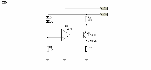
So why mention this method at all? Simply because the operation and characteristics of current sources are not well understood by most non-engineers (and quite a few engineers, too). Figure 1 shows a resistive current source that will maintain the set current of 1mA to an accuracy of within better than 1% over the range 0-10V.

The first thing that we need to be aware of is that the impedance is very high, and a perfect current source (as described above) does indeed have an infinite impedance. Although this is impossible to achieve in practice, impedances of many, many Megohms are quite possible, and are used regularly in many different circuit types. The actual impedance may be so high that PCB insulation resistance and transistor leakage current can become the determining factors. The values indicated with a * show the extreme case. With 1MV and 1GΩ, the current will be accurate (within 0.1%) with up to 1MΩ for R2. Few people will find this an attractive solution.
Simulators do have close to 'perfect' current sources, which are useful for comparing a real circuit with the ideal version, and they are commonly used to simplify complex circuits. Fortunately, real current sources are often close enough to being ideal in a real circuit that the difference is minimal.
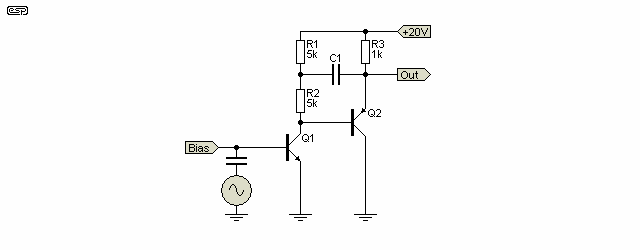
If we look at a simple common emitter transistor amplifier (Figure 2), the output impedance is equal to the collector resistance. This is a slight simplification, because the collector has a finite impedance as well, but for all intents and purposes the difference is tiny (less than 1% error in most typical circuits). The gain is roughly equal to the collector resistance divided by re - the transistor's internal emitter resistance. This is approximately equal to ...
re = 26 / Ie (in mA)
Naturally, re varies with the current, according to the above formula. Please note that biasing components have been omitted for clarity, but in reality they must be used because hFE is not a fixed number, and varies with current, collector-emitter voltage and temperature.
For all examples, a transistor with a current gain of 100 is used and the bias current will be set at exactly 100th of the expected collector current (using a simulated current source, naturally). In reality, a voltage divider or collector to base resistor is generally used to provide the necessary bias for simple single transistor circuits.
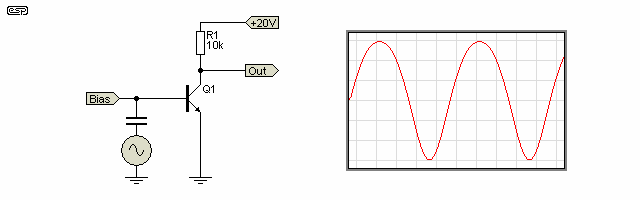
At low output levels, the gain should be 385, but as simulated is actually 333. This is well within the degree of accuracy we want to go to in this article, so practice correlates well with theory (one would hope so, or we would all be in trouble). With an output of 2V peak, the distortion is almost 5%.
As the transistors output voltage increases, the available collector current (and hence emitter current) falls, so re increases (and vice versa). The higher the output voltage (relative to zero volts/ ground), the less emitter current flows, and the lower the gain becomes. As the transistor turns on (reducing the output voltage), the exact opposite occurs, and the gain rises. This effect is immediately evident in the output waveform, which is distorted. This is shown in the oscilloscope trace in Figure 2, and the distortion is clearly visible, with the tops of the waveform flattened out, and the bottoms 'stretched'. This is typical of any transistor amplifier operating without feedback, and is also true of valves and FETs.
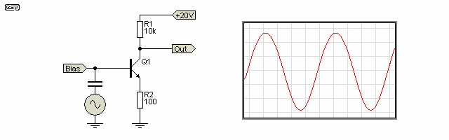
One method of reducing this distortion is to introduce a resistance into the emitter circuit (local feedback) to reduce the gain and swamp the variations in re. This works, and we still have a relatively low output impedance, but distortion is still evident - although much reduced. This is shown in Figure 3, where a 100Ω emitter resistor has been added.
A commonly held belief is that local emitter feedback (commonly known as degeneration) reduces the output impedance - this is simply not true - the output impedance of a common emitter amplifier is equal to the collector resistance, regardless of emitter degeneration. To reduce the output impedance, it is necessary to apply 'true' feedback around the entire circuit - from the output back to the input. The proof of this is outside the scope of this article, but it is nonetheless a fact.
With all this talk of distortion, I can almost hear all the thermionic valve (tube) enthusiasts cheering "I knew it - and here is the proof I have been looking for!"
Sadly, this is not the case. Valves do exactly the same thing, as do FETs of all types - the mechanism is different in each, but the result is the same. Gain varies with current in all known amplifying devices to a greater or lesser degree, so the principles outlined here are valid for any device. I am staying with bipolar transistors because they are the most commonly used of all the devices currently available. When 'trapped' inside opamps and other ICs you may not see them, but they are present nonetheless. Current mirrors can also be made using MOSFETs, but they must be carefully matched for Vgs or performance is rather poor.
In this case, the gain of the stage works out to be just over 76, and theory would predict a gain of 79, so again the correlation is very good. With an emitter current of 1.001mA (collector current plus base current), the value of re (literally 'little re') is about 26Ω, and this must be added to the external resistance Re. Remember that re still varies with current, and the external emitter resistor doesn't negate it completely. Distortion (again with 2V peak output) is reduced to 1.15%.
Since we have determined that the load resistance affects gain, and that variations of collector current (and hence emitter current) affect linearity, if a current source were to be used instead of the 10k resistor, we should get vastly more gain, and the distortion should be negligible. In this case, distortion (with no local feedback/ degeneration) is less than 0.5%.
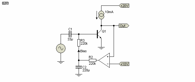
In reality, this is exactly what will happen, and Figure 4.1 shows a theoretical current source as the collector load. The current source is set to provide a current of 10mA (not 1mA as before). No oscilloscope trace is shown, because the linearity is so good that no distortion is visible, and a trace of an almost perfect sinewave gets tedious after a while. 

Figure 4.1 shows the circuit, which (theoretically) has a gain of about 3150. Naturally, real life will reduce this. Figure 4.2 shows the same circuit with a bias servo (which means that the chosen bias to maintain the desired collector voltage is retained). This form of circuit can no longer be biased using a simple voltage or current source, because the circuit gain is so high that even the smallest variation in transistor hFE, or the tiniest variation in a resistor value will cause the output to 'go to ground' or sit at the supply voltage.
Consequently, an opamp has been added to apply bias, otherwise the circuit is almost impossible to stabilise. The use of a bias servo in this manner is not too common, but it is used in a number of applications. Care needs to be taken to ensure that a low frequency phase shift oscillator is not created if you want to experiment with this idea.
Ultra-simple current sources (simply a transistor with the collector fed via a high value resistor from a high voltage) can work, but I'm not going to include one as they are not used in any sensible circuit. The current varies with voltage, temperature and depends on the transistor's gain. Now that the basic principles have been examined, we shall look at some real current sources (or sinks, depending on how you look at it).

| While a 'bias servo' is shown with these examples, when the high-gain circuit is subjected to global feedback, the feedback circuit provides the required DC conditions for correct biasing, and also provides AC feedback to allow the circuit to have predictable gain (set by the feedback resistors). The bias servo is necessary only when global feedback is not used and/ or for demonstration circuits such as those shown. |
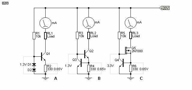
The two most common current sources are shown in Figure 5.1 (A & B), and are reasonably stable with transistor gains and temperature. Figure 5.1 (C) is shown simply because it may come in handy one day. While it does have extraordinarily high output impedance, MOSFETs are switching devices, and are not optimised for noise performance. Thermal stability is not wonderful either, because the BJT and MOSFET will never track each other. In audio work, absolute stability is not really necessary, since the feedback loop is used to ensure that bias voltages are maintained at the correct value. In some cases a DC servo circuit may be used (as shown in Figures 5.3 and 5.4), but this is not really necessary in the majority of cases. The DC servo is shown here because that's what was simulated, and it also helps to build an overall understanding of circuit techniques.
Figure 5.1 shows the two main variations used for current sources, with a MOSFET added for demonstration purposes. 'A' and 'B' are very common, and there are small variations as well. For example, a zener, LED or precision reference diode may be used instead of the two diodes. This may improve performance, but can also reduce the maximum voltage swing. Of the two, the dual transistor version is preferred by many (including me), as it has much better performance than the circuit using a diode reference. However, several projects have used an LED as the voltage reference because it takes up very little PCB real estate.
Note that in the following drawing, the load resistor is shown in bold, and this has been continued where appropriate. This makes it easier to differentiate between a 'functional' resistor (one that is necessary for the circuit to operate) and the load.
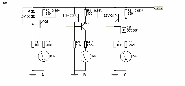
In each case, the 330Ω emitter resistor sets the current. Assuming that the diodes and transistors all have junction voltages of 0.65V, the theoretical current is ...
I = 0.65 / RE ( 0.65 / 330 = 1.97mA )
Where RE is the total emitter resistance - the internal re of the transistor plus the external resistance Re (the former was ignored for this demonstration, but the total resistance will actually be about 343Ω when re is included). In real circuits this is of little consequence, because the base-emitter voltage is not an exact figure. The reference current (via R1 or R3) should be between 10 to 20 times the expected base current to ensure stability. The MOSFET circuit is a little different in this respect, because the gate draws no current.
Both circuits have acceptable current stability as temperature changes, but both will change with temperature. The Vbe of a silicon transistor varies at about 2mV/°C, and this causes the current to vary accordingly. It's almost always a good idea to keep current sources well away from components that run hot, and especially so if the temperature is not consistent. I say 'almost' because sometimes you may want to use the variation to measure temperature for example (and yes, these circuits can work well as thermal sensors, although they are far from being precision devices).
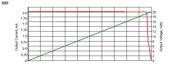
The above graph shows the current vs. output voltage, using the two transistor source shown in Figure 5.1 (B). Provided the output voltage is less than 19.2V (a resistive load of 9.8k or less), the full current of 1.97mA is available, and it falls off quickly with higher load resistors. This is to be expected because there's only a 20V supply for the current source, and it can't provide the full current into a resistor if the output voltage would equal or exceed the supply voltage (less the voltage across the current sense resistor R3 and at least some voltage across the transistor).
If operation into a higher resistance is necessary, then the current must be reduced or the supply voltage increased. One must always ensure that the combination of voltage and current (i.e. power) does not exceed the maximum rating for the transistor. It's obvious from the graph that the circuit continues to function even when the emitter-collector voltage across Q2 is almost zero. Almost the full current (1.89mA vs. 1.94mA) is available with only about 120mV across Q2.
The output impedances of the 'A' and 'B' versions of current source are tabulated below, over a wide range of load resistances. Temperature is assumed to be 25°C, and the current varies with temperature - even if the transistors are thermally bonded.
| Transistor + Two Diodes | Two Transistors | ||||||
|---|---|---|---|---|---|---|---|
| RL1/2 | Current mA | Voltage | Impedance | Current mA | Voltage | Impedance | |
| 0 | 2.3020 | 0 | n/a | 1.9516 | 0 | n/a | |
| 1 k | 2.2967 | 2.2967 | 433 k | 1.9506 | 1.9506 | 1,951 k | |
| 2 k | 2.2912 | 4.5824 | 833 k | 1.9496 | 3.8992 | 3,899 k | |
| 3 k | 2.2851 | 6.8553 | 1,124 k | 1.9484 | 5.8452 | 4,871 k | |
| 4 k | 2.2774 | 9.1096 | 1,183 k | 1.9471 | 7.7884 | 5,991 k | |
| 5 k | 2.2718 | 11.3590 | 2,028 k | 1.9457 | 9.7285 | 6,949 k | |
| 6 k | 2.2644 | 13.5864 | 1,836 k | 1.9442 | 11.6652 | 7,777 k | |
| 7 k | 2.2563 | 15.7941 | 1,950 k | 1.9424 | 13.5968 | 7,554 k | |
| 8 k | 2.2476 | 17.9808 | 2,067 k | 1.9405 | 15.5240 | 8,171 k | |
| 9 k | 2.1269 | 19.1421 | 159 k | 1.9383 | 17.4447 | 7,929 k | |
| 10 k | 1.9188 | 19.1880 | 92 k | 1.9205 | 19.2050 | 1,079 k | |
The average impedance (excluding the lowest and highest currents) is 1,432k for the diode referenced source and 5,895k for the two transistor version. Quite clearly, the two transistor current source has much better linearity over a wider range, but this level of accuracy is not usually necessary - although it doesn't hurt either. The primary benefit is that the impedance is a great deal higher - it remains above 1Meg at all output loads, right up to the point where there is only 0.15V remaining across the transistor (Q2). The circuits shown below use both types of current source.
I didn't include the MOSFET version in the above table, because for all intents and purposes its output impedance is infinite. According to the simulator, Zout is around 250GΩ, and while I don't necessarily believe the simulator implicitly, several different versions of the circuit were tested and gave similar results. You can reliably expect the output impedance to exceed 2GΩ under any realistic conditions. The BS250P shown is a small-signal P-Channel MOSFET, and is (roughly) the P-Channel equivalent to the 2N7000 (N-Channel). One disadvantage is that the voltage across the MOSFET needs to be a little higher than across a BJT. With less than 1V (drain to source) most MOSFETs will lose much of their gain (transconductance).
One may well ask the question: "How do you calculate the impedance of a current source?" The method is not immediately apparent, but it has nothing to do with the voltage across the transistor and the current through it. You may imagine that this would give you the answer, and while it does give an answer, it's wrong. You need to measure the voltage across and current through the load, then change the load slightly and measure again. This gives the 'delta' ( Δ means change ) of the two values.
As an example: If the load is 10k and the current is 1mA, there must be 10V across the resistor, assuming the values are exact. If you change the resistance to 9k, you expect 9V, but it will be ever so slightly higher because the transistor has finite gain. Let's assume that the voltage across 10k is exactly 10V, and the voltage across 9k might measure 9.005 volts. We use this difference to calculate the dynamic output impedance of the current source ...
ΔV = V1 - V2 ( 10 - 9.005 = 995mV ) ΔI = I1 - I2 ( 1.0006mA - 1mA = 600nA ) Zout = ΔV / ΔI Zout = 995mV / 600nA = 1.66 Meg
The output impedance (Zout) of the current source is therefore 1.66 MΩ. The calculations are tedious, even using a simulator which gives results that are more accurate than most normal test instruments. As you should expect, the voltage across a lower resistance is ever so slightly higher than it should be, and vice versa. A perfect current source would show identical current through the load resistance, regardless of value. This calculation is only an example, and is not related to the figures shown in the above table. However, now you know how the values in the table were determined.
As a further example, imagine an 'ideal' 2mA current source, a device that exists in most simulators, but not in real life. The voltage across a 1k resistor will be exactly 2 volts. With a 900Ω load (for example) the current is unchanged, but the voltage is now 1.8 volts. We have ΔV (200mV), but no ΔI, therefore the above calculation will produce a 'divide by zero' error, and the answer is infinity (∞). This is obviously not possible in the 'real world', even if the current source were derived from a very good opamp. I've shown an example circuit in Figure 5.2.1.
The change in load resistance must be appropriate for the current source being measured, to ensure that the load voltage is well within the allowable range for the circuit being measured. Ideally, the voltage across the load will be roughly half the supply voltage for both parts of the test described.
5.01 - Current Sinks
There is no real difference between a current source and a current sink, other than terminology. We tend to think of a current sink as being connected to the common (zero volts/ ground) and 'sinking' current from the supply. The circuits shown in Figure 5.1 can simply be inverted (and semiconductor polarities reversed) to obtain the equivalent current sink. The nominal current is set by R2, R4 or R6, and is about 1.97mA (assuming 0.65 base-emitter voltage). It varies with temperature, and this needs to be considered in some cases. Figure 5.1 is no different in this respect.
It's clear that there is no real difference in the circuits themselves, other than the polarity reversal. The load is referenced to the positive supply rather than ground, but otherwise performance is identical, at least in theory. There's no point showing the impedance table, as it's very similar to that shown in Table 1. There will be some small variations because NPN and PNP transistors are always a little different - even when indicated as complementary. This is rarely a problem in normal circuitry.
Using a current source as the load for a transistor (or JFET) increases gain and improves linearity. It's a surprisingly common technique, but it's not always obvious that there is a current source or it's purpose. Current sources can also use an opamp, especially if a particularly accurate current is needed. The gain of the opamp ensures that the current is very stable, and with low input offset opamps (or with offset trimming) the current can be very accurate. An example is shown below.
These both include a 'DC servo' (see DC Servos for more information). This is included because without feedback, the gain is so high that no 'normal' biasing scheme will be stable enough to keep the output at (roughly) half the supply voltage.
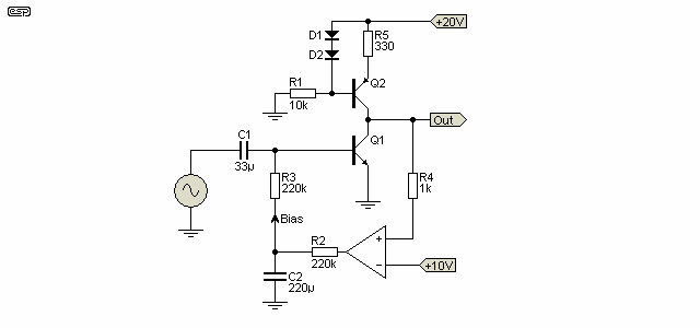
The voltage drop across the two diodes remains relatively constant (ignoring thermal effects). This means that the collector current of the current source is determined by the base-emitter voltage. 0.65V exists across R5, and this sets the collector current. The formula for setting up both current sources is shown below.
The gain of Q1 is relatively unaffected by the change in the configuration of the current source. In either of these cases, the inclusion of an emitter resistor in the gain transistor (Q1 in each drawing) reduces the gain, but the change is far less than would be the case with a resistive load. Remember that the output impedance of the current source is extremely high, so adding emitter resistance has far less effect than with a 'conventional' single transistor amplifier stage.
The two transistor current source is one of the most commonly used, and has acceptable stability. Thermally bonding the transistors doesn't help a great deal. High stability is not needed for most applications, since as mentioned previously, absolute current accuracy/ stability is not (or should not) be a requirement for an audio amplifier.
This is a very simple circuit, but will give very good results wherever it is used. Current is calculated by (approximately) ...
I = 0.65 / Re
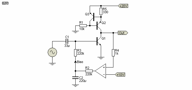
In this case, the internal emitter resistance (re) is not an issue, since the second transistor (Q3) allows only that exact amount of base current for the current source (Q2) to develop 0.65 Volt across the resistor. Should the current try to increase, Q3 simply turns on harder, and steals more of the base current. The current through Q3 should be at least 10 times as great as the expected base current of Q2 (the current source).
With all the circuits shown, output impedance is very high, and by my tests is about 8.2k. Inclusion of the emitter resistor (providing local feedback) has only a very small effect on the output impedance - it primarily reduces the gain.
It is not uncommon to see a single reference transistor (Q3 in Figure 5.1.2) controlling two or more current sources (which may be supplying different currents). The reference should always control the current source transistor that has the most stable current. For example, if there were a current source for the input stage and the Class-A amplifier, the reference should always be taken from the source used for the input stage. This minimises any possible cross-coupling between the two current sources.
For many precision measurement applications, a very tightly regulated current is often needed. It will typically also be calibrated to ensure that the current (with load resistances within its range) does not vary by more than perhaps 0.1% or less. The best way to achieve this is to use an opamp.
In the following drawing, you may be puzzled by the secondary supply for the opamp. This was used because most opamps cannot cope with the input being so close to the supply rail. They show their displeasure by not working well (if at all), and the auxiliary supply ensures that there is more than enough voltage between the two inputs and the opamp's supply to ensure reliable operation. If you wish to experiment with this circuit, you must include the auxiliary supply!
It's unlikely that you'll need anything like the precision that the above circuit can provide, but it has performance that will exceed that of the simple transistor or transistor/ diode versions, depending on the implementation. The current with the circuit shown (using a TL071 opamp and a BC559C transistor for the simulation) varies by 30nA when the load resistor is changed from 2k to 2.2k, and using the formula shown above that means that output impedance exceeds 14 MΩ. The circuit shown is significantly better than the two transistor version described above, but there is still some variation. The culprit is the transistor's base current, because even though the voltage across R2 barely changes at all, the base-emitter junction provides a little more current through R2 as the load changes. Best results are obtained when the transistor's hFE is as high as possible. A PNP Darlington is recommended for the highest possible output impedance (well over 100 MΩ is possible).
Alternatively, a P-Channel MOSFET can be used, and the output impedance will be immeasurably high - even with the simulator ! It's doubtful if you need to ever go that far, but I have used a similar arrangement in the Project 168 - Low Range Ohmmeter article. Rather than diodes, a precision voltage reference diode is used in the project article for improved stability, along with a low-drift opamp. As shown, the use of diodes as a reference detracts from the 'precision' description, because their voltage drop varies with temperature.
The final (and least understood) of all the current sources is the so-called 'bootstrap' circuit. While not as good as an active current source, its performance is still more than acceptable, and in the example shown in Figure 5.1.1 manages to provide a gain of 8,860. This is at a current of only 1mA (some of the other circuits shown use 2mA), so the gain is reduced a little. However, this circuit is not in the same league as the gain of millions from the current source, but in real terms its performance is more than enough for the Class-A amplifier / driver stage of a power amplifier.
There are some advantages and disadvantages to this circuit, and it is dependent on the application whether it will be suitable. Where a true current source has the same (more or less) impedance at all frequencies right down to DC, the bootstrap circuit has a low frequency cut-off point determined by the resistance and capacitance used. This makes DC biasing easier (since the gain is quite low at DC), but since it reduces gain (and global feedback) slightly at DC, there may be a little more DC offset at the amplifier's output as a result.
Distortion will also increase at very low frequencies, since the constant voltage across resistor R2 will not be maintained as phase shift (and LF rolloff) start to take their toll. If the bootstrap capacitor (C1 in the circuit below) is made large enough, the low frequency performance is not compromised to any measurable degree.
One of the benefits of the arrangement is that the voltage at the junction of R1 and R2 can exceed the supply voltage. This is especially useful if the circuit is driving MOSFETs, as it can provide the necessary extra voltage to drive the gates without an auxiliary supply. Unfortunately, this little trick only works with one polarity unless a 'double bootstrap' circuit is used. . The other benefit is simplicity - passive components that are operated well within their ratings have an indefinite life. It is extremely rare for a bootstrap capacitor to fail - I have even seen a circuit where the cap was installed with reverse polarity, and the amp was working fine. Where current sources can be damaged if an output device fails, the bootstrap circuit won't.
Since it is so misunderstood, it is worth a few words of explanation. R1 and R2 supply a nominal current of 1mA (resistors are 5k each). Under normal (i.e. quiescent) conditions, there will be 5 Volts across each resistor. As the output varies, the capacitor couples the output signal back to the centre tap of the two resistors, and if the emitter follower were a perfect buffer amplifier, this would exactly equal the input. As a result, the voltage across R2 is kept constant - if the voltage across a resistor is constant, then it follows that the current through the resistor must also be constant. The current through R1 varies considerably, but R2 maintains a constant current over the full output operating range.
Small differences in voltage (due to the loss through the emitter follower) or in phase (due to the capacitive reactance starting to become significant with decreasing frequency) both cause the bootstrap current source to reduce its effectiveness, so impedance and gain drop, and distortion increases. In a well designed circuit, these effects are minimal at all normal operating frequencies, but cannot be discounted. This circuit has been used in several ESP power amp designs, all of which have proven to sound very good in the roles for which they were designed. Project 3A and Project 101 are examples of true hi-fi designs that use this technique. Despite claims that it's not as good as a 'real' current source, it's highly unlikely that anyone could pick the difference in a blind test.
Note that the bootstrap circuit requires some form of unity gain output stage to function. It cannot be made to work with a single stage. An example of a simple preamplifier using the bootstrap technique can be seen in Project 13, and I designed the circuit many, many years ago as a microphone preamp. It's still a viable proposition, despite the proliferation of low noise opamps.
Where the requirements are not too demanding, a junction FET (JFET) can be used as a current source. Although the performance of the JFET itself is quite good, there is a significant variation between FETs in the all-important gate-source voltage. This means that if a fixed resistor is used as shown in Figure 5.4.1, the current will vary depending on the FET characteristics. Depending on the circuit, this may or may not be a problem.
For circuits that have some kind of feedback to stabilise the DC operating conditions, current variations are relatively unimportant, but when a specific current is needed, R1 must be a trimpot or be selected to provide the current required. Most JFETs are limited to relatively low currents - typically no more than about 5mA, but that depends on the type of FET and the allowable dissipation. A simulation using BF245A/B/C JFETs with R1 set at 560Ω gave currents of 1.38, 2.03 and 4.46mA respectively, demonstrating that the part number suffix is significant.
The dynamic resistance is calculated quite simply, by measuring the change (Δ) of voltage and change of current. If the voltage is varied over a range of (say) 10V and results in a change of current of 100µA, the dynamic resistance is 100k.
RD = ΔV / ΔI
RD = 10 / 100µ = 100k
Some FETs can be used with no resistor at all. The current is then 100% dependent on that particular FET's characteristics, and can vary widely even with the same type of FET from the same manufacturing batch. Despite the apparent disadvantages, there are many uses for JFET current sources and they provide acceptable performance for many applications. In most cases (but by no means all) the dynamic resistance is improved (made greater) by using a source resistor. The best performance is achieved when the programmed current (I D) is much less than the maximum (I DSS). Fig. 5.4.1 is an example only, and the dynamic resistance and current are from a simulation.
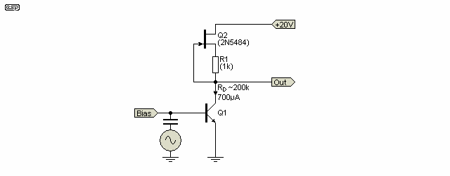
Q1 is shown as a BJT, but it can be a JFET, MOSFET or even a valve (vacuum tube) if the voltage is within the range of the JFET. The performance of the current source shown above is best described as 'respectable', rather than good or excellent. Provided there is enough voltage across the JFET the current is reasonably stable, but it falls rapidly if there isn't enough voltage for the FET to bias itself. The voltage across R1 depends entirely on the FET, and may be anywhere from a couple of hundred millivolts to a volt or more. Output impedance ('dynamic resistance') depends on the transconductance of the JFET, but you can expect it to be better than 100k. This isn't even close to the transistor versions, but it does have the benefit of relative simplicity.
One of the reasons you don't see discrete JFET current sources/ sinks used very often is their extreme variability. Unless the design is either very tolerant or warrants a trimpot to allow the current to be set for a specific value, a JFET is generally unsuitable. Most are also fairly low voltage (30-40V is common), and are unsuited to high voltage circuits. While high voltage JFETs may be available, they will be significantly more expensive and harder to get than bipolar transistors which will give better performance anyway. The range of suitable JFETs has diminished considerably in recent years, with some of the better ones having gone completely (they are now obsolete, and those you buy from Asia will probably not be anything like the originals). There are still a few linear (general purpose) types available in SMD packages. These are hard to work with if you're experimenting.
Common switching JFETs such as the J111/2/3 can be used as 'constant current' sources. I've not verified it, but the simulator claims that high-frequency performance extends to at least 10MHz. These are some of the very few through-hole types that remain readily available (and cheap) from most suppliers. Being switching FETs, they are characterised by their 'on' resistance (RDS (on)), and while their other parameters are provided, they're not particularly useful for this application.
There are several 'current diodes' available (some are referred to as a CRD - current reference diode or CLD - current limiting diode) that can be used where the current is not particularly critical. They aren't really diodes at all, but are a basic current regulator using a JFET, in a diode or 2-pin TO-92 package. Unlike the JFET current sources described above, CRDs are 'batched', so are tested for their current and marked according to the current passed at the test voltage (typically 10-25V). Like a JFET, their performance varies with applied voltage and temperature. They are available from a number of manufacturers, but they are not precision devices.
The LM334 (or 134/ 234) ICs are a better option where precision is required. These are 3-pin devices, with a 'current set' pin that allows the user to preset the current required using a resistor or trimpot. The datasheet shows the formulae needed to determine the current. Because these are ICs, they come with many of the issues faced with any IC, such as an absolute maximum voltage (30-40V) and a limit on the slew rate they can handle, which is quite low (1V/ µs at 1mA). This means that they are (generally) not suitable anywhere that there are fast transitions. However, for static applications they are much more accurate than current diodes or most other techniques.
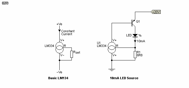
There are tricks that can be used with these devices, as shown above. The device current is defined as a ratio between the required current and Iset (the current drawn from the 'set' pin). The nominal value is 18 - the output current is 18 times the set current, but this varies with the set current and temperature. The LM334 has a fairly significant temperature dependence, approximately 227µV/°C. This is a nuisance, but the datasheet shows how it can be mitigated by adding a diode and resistor. The datasheet even includes an application using the LM334 as a thermometer.
Not quite so obvious from the datasheet is that the voltage at the set pin (relative to the V- pin) is about 68mV. Knowing this allows you to use the device in 'interesting' ways, as shown in the datasheet, and in the second drawing of Figure 5.5.1 (attributed to Bob Pease). Note that if (when) you see on-line videos covering the LM334, many of them are misguided, and one person (apparently) had the audacity to claim that Bob Pease was wrong. That's always a big call, but the commentator was wrong, bot Bob. You may well ask why the extra transistor has been included, but it's to keep the current through the LM334 to the minimum, meaning that there's almost no self-heating.
All current sources/sinks require a voltage reference, with the exception of those based on a JFET. While most discrete circuits use a diode, transistor junction or a LED as a voltage reference, these all have (often significant) variations with temperature. Most of the time, this actually doesn't matter much - an audio amplifier is not a precision instrument, and the variations experienced will rarely cause any problems (I have never seen an issue with a current source in any audio application). The LM358 or TL071 are generally suitable, and they are inexpensive (less than AU$1.00) but have very good performance (especially at low frequencies).
Current 'diodes' use a JFET, and the voltage reference is the gate-source voltage. This isn't particularly accurate and is temperature sensitive, but in many applications this doesn't matter. If all you need is a high impedance current source/ sink, but the actual current doesn't matter too much, then they are fine. For precision, a better (and more predictable) voltage reference is needed.
ICs, and especially those used for voltage regulators or other precision applications, generally use a band-gap reference (see Reference 1). While these can be made using discrete devices, their performance will never be very good. Because the transistors in an IC are all on the same substrate, and are generally well matched (and thermally coupled), the performance of IC references is far better than you will obtain from discrete circuits. Since absolute accuracy is never needed for audio applications, use of discrete band-gap voltage references is not recommended. If you do need that degree of accuracy, use a commercial IC voltage reference IC - it will be far better than one you build using separate transistors.
Now that we have looked at the various types of current source (there are many more, but the others will not be examined here), we can examine where they are best used, and why.
I have always been interested in audio amplification, and will therefore concentrate on this aspect of the use of current sources and mirrors. There are naturally countless other applications, but I will leave it to the reader's imagination to explore the additional uses. A few common uses include timers, power supplies (discrete), instrumentation amplifiers (which often operate within the audio range), and industrial process controllers, but this is a small subset of the uses. Almost every linear IC ever made uses current sources/ sinks extensively.
One of the most irksome loads for any amplifier is one that has inherent non-linearities, and the output stage of an audio amp definitely fits this description. Consider the worst case, where there is no forward bias applied to the output devices, which are operating in Class-B. The global feedback in an amplifier is generally considered to the be main saviour, by reducing the distortion components by using the input stage as an error amplifier.
This is actually only a small part of the story - a properly designed Class-A amplifier will have both high gain and high output impedance, both of which are useful in reducing the otherwise inevitable crossover distortion. Consider Figures 6.1 and 6.2, showing the same output stage delivering the same peak output voltage to the same resistance.
The first is using a low impedance amplifier (an opamp) with unity gain as shown, but will normally be adjusted to give the required output, while the second uses a high impedance source having a impedance output, but still providing the same output voltage. The amplifier stage in Figure 6.2 (Q3) has considerable gain, but this is not important for the demonstration.
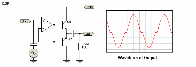
The load for each amplifier is 100Ω, and it is clear from the first figure (6.1) that crossover distortion is gross. Figure 6.2 shows how the high impedance drive to the output stage overcomes the crossover distortion - the output waveform is not shown, because there is virtually no distortion visible in the oscilloscope trace, so it looks just like a sinewave. This doesn't mean that it has no distortion though - it's just not visible in a trace.
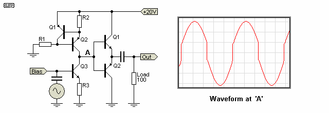
Remember that this is with no feedback whatsoever - the addition of feedback will reduce the distortion even more - as will some biasing on the output stage. Neither of these were included to show the effect more clearly. Note that the settings on the oscilloscope were not changed between these simulations, to ensure that the full effect was not obscured (or accentuated) for each example.
The inescapable conclusion is that the high impedance drive will greatly assist in overcoming non-linearities in the output stage, even those as nasty as a completely unbiased complementary pair as shown. Naturally other non-linearities are also negated (to some degree) by these techniques, which are pretty much universal in modern amplifier designs. Using the high impedance Class-A stage with feedback cannot eliminate crossover distortion though! When the output transistors are not conducting, there is no feedback. This happens because non-conducting transistors have no gain, so the overall gain of the amplifier will be extremely low. Feedback can only work when the amplifier stage has overall gain!
None of the above should be taken to mean that we no longer need negative feedback - the idea is to make the amplifier as linear as possible before feedback is added. This makes a good amp better - feedback will never make a bad amp good !
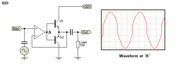
If an opamp is used with the feedback taken from the output, it's effective output impedance is extremely high, and it works exactly the same as the circuit shown in Figure 6.2. The waveform at point 'A' is the same, and the opamp's high gain allows the circuit to work better than expected. However, the performance at high frequencies will be poor, and this is a case where adding feedback does not make a 'bad' amp into a 'good' amp.
Of particular concern is that when the two output transistors are biased off, the circuit has no (or very little) gain. If a circuit has no gain, it stands to reason that it also has no feedback, so this scheme can never provide acceptable performance. Biasing the output devices are essential to ensure that they always have enough gain to get a linear output. Many modern transistors have very good gain linearity even at low current, so it's not hard to get the output stage to work with reasonable linearity.
The next item is current mirrors, another little understood circuit. These are extremely useful in amplifier design, and in this section I will show where they can be used, and the benefits that can be obtained.
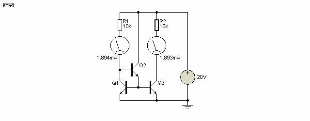
The basic current mirror is shown in Figure 7.1, and it can be seen that whatever current is injected into the left side is mirrored, and the right hand side is a constant current source (sink) reflecting the injected current. Should the input current at change, so will the output current, but it will remain constant, regardless of the actual voltage (provided it remains within the supply limits of course).
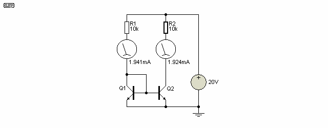
The problem with this circuit is that the current in the two halves is different - the mirrored current is too low, differing by 19µA (it is actually 20µA, but the simulation accuracy used was not great enough to show this). If we check, we will find that the emitter currents of both transistors are identical, so the 20µA that 'disappeared' is the base current that must be supplied to each transistor (10µA each).
Adding emitter resistors does absolutely nothing to alleviate this, but is useful if the transistors are not matched. Even then the resistors do not really do a lot of good, unless the voltage developed across them is significant (at least 100 mV, and preferably more) but it helps a little bit.
A better solution is to use a buffer as shown in Figure 7.2. This removes the base current component of the error, and makes the current mirror matching a lot better. This simple addition has reduced the error dramatically, but it can be improved even more. While not generally needed for audio amplification, improved performance is essential for test and measurement, or other critical applications.
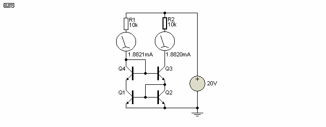
As you can see from the above, Figure 7.3 [ 1 ] is almost perfect - the current balance is extremely good. While this arrangement is used in analogue opamps and other circuits requiring high precision, there would be no advantage using it in a power amplifier. There simply is no need for such precision. It will not generally improve distortion, bandwidth or dynamics, but may give a marginal improvement in DC offset (which can be up to 100mV without causing any problems whatsoever in most power amps used for audio). All we need to do now is find a use for these circuits.
Note that I have shown current mirrors with extremely good matching, but this depends on the transistors being matched as well. With discrete circuits, matching to the required levels is somewhat tiresome, and unless you are building a precision circuit (which will typically use a transistor array to ensure matching and thermal coupling), it usually doesn't matter. The simple mirror shown in Figure 7.1 is perfectly fine for most applications.
Consider the differential pair (aka long tailed pair or LTP). Most of the time, we are losing half the gain of the circuit, since the output is taken from only one collector as shown in Figure 8.1. This configuration also suffers from linearity problems, unless the output is current only - as is the case when driving the base of a transistor (this is shown further below).
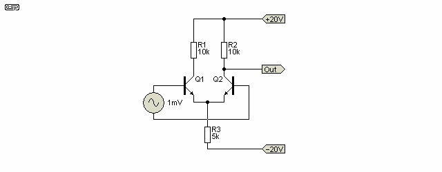
The circuit as shown (without the essential biasing components, which were omitted for clarity) has a voltage gain of 285 (again using transistors with a hFE of 100), and is quite linear at low output voltages. The linearity will suffer badly as the level increases, and even with the ±20 volt supplies used is not satisfactory (10% THD) as a voltage amp for outputs greater than 1.35 Volts RMS (this is at an input voltage of 5 mV).
Using a current source / sink in the 'tail' is very common in amplifier circuits, and this variant is shown below. It is commonly (but entirely mistakenly) assumed that this increases the gain (in the circuit shown, gain is reduced to 168), but the real purpose is to improve the common mode capability of the circuit. Common mode signals are those that are applied to both inputs in the same polarity, and are generally required to be rejected. Using a simple resistive tail severely limits the common mode voltage that can be accommodated before severe distortion occurs, and indeed the common mode rejection of the circuit is almost useless.
In the example above, the common mode rejection is well under 1dB but with a current sink tail the rejection is almost 65dB. In most amplifier circuits common mode signals (of the undesirable kind) are not an issue if the input stage is properly designed. Although a high common mode ability is usually considered necessary, this is not always the case. For a typical power amplifier, the common mode voltage cannot exceed the input voltage for full power. There are other good reasons to use a current source/sink though, one of which is to ensure that circuit stabilises at a low voltage, eliminating (or at least minimising) switch-on / off thump.
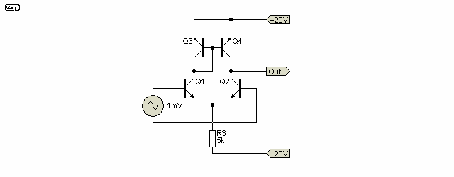
If a current mirror is used as the load, gain is increased by a very useful amount, and Figure 8.2 shows the arrangement used. The stage gain is now 850 and the use of a current sink as the tail has no effect (provided that the current is maintained at 4mA). This circuit is shown in Figure 8.2, and although useful in certain applications, it is not suitable to drive the output stage of a power amplifier.
If we really wanted to get silly (and I have seen it done), we can put all the bits together in one place, and finish up with an input stage + Class-A driver, with a total open loop gain (i.e. without feedback) of 33,800 or 90dB (but still loaded with 100k). This will not increase dramatically when the output is buffered - the output impedance is actually reasonably low, at about 4k. The buffered current mirror does not help the gain, but reduces output offset. The complete circuit is shown in Figure 8.3, and is a useful example of the techniques discussed in this article. Open loop distortion is about 5% at 6V RMS output, but will fall dramatically when feedback is applied.
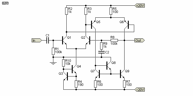
This circuit uses an input LTP that drives a secondary LTP as the Class-A amplification stage. The load for this second LTP is a current mirror, and this arrangement has excellent linearity. I suspect that it could be a cow to stabilise in a real amplifier circuit, and quite frankly, I do not see any reason to go this far. Many amplifiers have been designed using this arrangement, and it's very common with MOSFET output stages. Initial measurements on a MOSFET amp using this drive stage show that stability is not as good as I would like to see (there are traces of oscillation at some output levels), but overall stability seems to be acceptable. I expect that the wide bandwidth of the MOSFET output devices might make this arrangement a little more tractable than would be the case with bipolar transistors. I have not found it to be necessary though, and the P101 MOSFET amp does not use this input/driver stage combination.
At this stage, I suspect that I have either cleared up some degree of confusion, or created even more. There are so many choices, and so many reasons to use (or not use) any one of them. This article is meant only to describe and explain - you can see where my own preferences lie from the circuits published in the projects pages. I happen to be a strong supporter of the KIS principle (keep it simple), and in my own designs have not found it necessary to make the circuit any more complex than is needed to make it work and provide good performance, worth of the term 'hi-fi'. Listening tests bear this out, and IMO I do not believe that the difference between a highly complex amp and a simple one (provided that both are well designed) is audible under any listening conditions.
This being the case, I cannot think of any good reason to go for the complex solution, especially since it will almost certainly be much harder to stabilise (I happen to think that this is extremely important), and will use more parts. Granted that the additional cost is minimal in the greater scheme of things, but sound for sound, simple and reliable has to win out.
As a final point, with the LTP configuration and current mirrors, it is often beneficial to match the transistors, so they have gains that are approximately equal, and emitter-base voltages that are as closely matched as possible. It is also useful with both of these configurations and two transistor current sources to thermally bond the two transistors to prevent mismatch due to thermal effects.
Remember that the emitter-base voltage of a transistor falls at a rate of 2mV / °C, so even a small temperature difference will change the DC offset performance of a long tailed pair or current mirror quite dramatically. Thermally bonding the transistors minimises the offset, but does not affect any current variation caused by the change of temperature. The current is usually not critical, so a small variation is usually of little or no consequence for audio applications. Test and measurement systems generally require much greater performance, otherwise they may provide results that aren't useful.
For more information on the design of amplifier stages, please refer to the Amplifier Design page.
Most of the circuits shown are reasonably generic, and although I obviously found them somewhere, it was a very long time ago. As a result, most of the material isn't referenced to anything in particular, as it can be found in many books, websites, existing circuits, etc.
Main Index
Articles Index