
|
|
| Elliott Sound Products | Project 3A |
 Please Note: PCBs are available for the latest revision of this project. Click the image for details.
Update - 25 June 2009 - Although the last update highly recommended the latest OnSemi power and driver transistors, they remain hard to get in most countries. As a result, the recommended power transistors are now the much more readily available MJL21193/4. While in theory these are not quite as good as the latest versions, they are still excellent devices. It is extremely doubtful that anyone would ever pick any difference with test instruments, and there will be no change that is audible.
Much the same applies to the driver transistors. Although the BD139/140 devices are not considered to be the 'finest' audio transistors available, they work very well indeed, and have been used in all of the P3A amps I've built for my own use or as part of a system. Again, it is highly unlikely that there will be any meaningful measurement that will show these transistors to be inferior to 'audiophile' parts.
24 Jul 2003. - OnSemi released a new range of transistors, designed specifically for audio applications. These new transistors have been tested in the P3A, and give excellent results. As a result, all previous recommendations for output transistors are superseded, and the new transistors should be used ... if you can get them. Several years after release, the new devices may still not be readily available.
The output devices are MJL4281A (NPN) and MJL4302A (PNP), and feature high bandwidth, excellent SOA (safe operating area), high linearity and high gain. Another output transistor option is the 200W NJW3281 (NPN) and NJW1302 (PNP). These also have excellent specifications. You can use 2SA1943-O(Q) (PNP) and 2SC5359-O(Q) (NPN) transistors, but only if purchased from a major distributor. If you get them from eBay or the like they will almost certainly be fakes. Driver transistors are MJE15034 (NPN) and MJE15035 (PNP). All devices are rated for at least 250V, with the power transistors having a 230W dissipation (except 2SA/SC devices, 150W) and the MJL drivers are 50W. BD139/140 transistors are rated for 8W.
For a budget system, you can use TIP35C (NPN) and TIP36C (PNP) output transistors. If you can get the 'full-pack' TO-247 case versions they can be mounted under the board in the same way as the MJL devices. These are limited to 125W dissipation (25°C case temperature), but despite that apparent limitation they can still drive a 4 ohm load from ±35V supplies. In theory the peak dissipation may be exceeded, but these are extremely rugged transistors and handle abuse with ease. Don't push your luck though - the maximum unloaded supply voltage is ±35V!

| Note that there is a major reason that P3A is different from most amp projects you will see on the Net - it uses complementary feedback pairs (aka Sziklai pairs) for the output stage, and quiescent current is controlled by the driver transistors. If the bias servo is mounted on the heatsink, it will provide over-compensation and crossover distortion will result. |
The basis for this amplifier was originally published as Project 03, and although the base design was developed over 40 years old, as an amplifier it remains an extremely good amplifier. It is simple to build, uses commonly available parts and is stable and reliable. The design featured is a full update on the original project, and although it has many similarities, is really a new design.
This new amp (like the original) is based on an amp I originally designed many years ago, of which hundreds were built. Most were operated as small PA or instrument amps, but many also found their way into home hi-fi systems. The amp is perfectly capable of driving 4 Ohms, provided the supply voltage is maintained at no more than ±35V.
This amplifier, although very simple, is capable of superb performance. This is not an amp to be under estimated, as the sound is very good indeed, and this is due (in part, at least) to the inherent simplicity of the design. The amp is exceptionally quiet, and is reasonably tolerant of difficult loads. It is an ideal amplifier for biamped systems, and may be operated in bridge mode (BTL) if you use the recommended output transistors (which have the necessary power ratings).
The design has had the benefit of many, many years of consistent use, and this version is the best of all - the refinements ensure minimum 'switch-on' or 'switch-off' noise, and the availability of really good output devices has improved on a known and very stable design.
I have heard nothing but praise from those who have built this amplifier - all feedback I have received has been very positive indeed. It is highly recommended, based on the reports from countless people who have built it. Considering that the design has been available for 20 years with almost no changes (other than output transistor changes due to availability), it's safe to say that it has stood the test of time. It makes no pretense at being 'better' than anything else, but the results of several thousand constructors is testament to its inherent reliability and sound quality.

Photo Of Completed Revision-C Amplifier
The photo above shows how the board mounts to the heatsink and clamps the output transistors beneath the PCB. This is the latest Revision-C version of the PCB, but the general arrangement hasn't changed very much over the years. It's always been possible to cut the topmost section of the PCB so the output transistors can be mounted vertically, and the board can also be cut in half so each amp can be on its own heatsink or even in a separate enclosure. You may notice that the photo shows 0.22 ohm emitter resistors and the schematic shows 0.33 ohms. The higher value is recommended as it improves bias stability.
For those who want to build a Class-A power amp, see Project 3B. It is virtually identical to the design shown here, but needs a far more robust power supply to accommodate the high quiescent current. Although most people seem to think that Class-A is 'better' than Class-AB, it's not really the case. P3B has performance that's really no better than the P3A, but has far less power and develops a great deal more heat.
Note that like the original, there is (still) no output short circuit protection, so if speaker leads are shorted while the amp is working with a signal, there is a very real risk of the transistors being destroyed. I suggest and recommend the use of Speakon connectors both at the amplifier and speaker ends. The specifications are very similar to those of the original project, but the use of a current sink in the differential pair input stage means that there is virtually no thump at turn on or off.
I have also added the ability to adjust the quiescent current, and with the transistors specified the amp will provide 100W into 8 ohms, at a maximum supply voltage of ±42V. This supply is easily obtained from a 30-0-30V transformer. Consider that increasing the supply voltage from 35V to 42V represents an output power increase of only about 1.6dB, but the potential for output transistor damage is almost doubled. IMO, it's just not worth it.
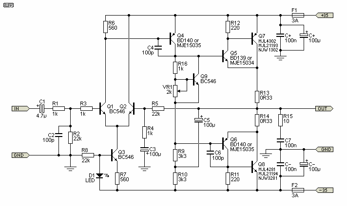
Figure 1 - Amplifier Schematic
As can be seen, it is not a complex amp, but the performance is excellent. Part of the design was to ensure that it will work with a variety of transistors without other modifications. This can only be achieved with a simple design - the more complex the design, maintaining stability (freedom from oscillation) becomes much more difficult, and it will only work with the exact transistors specified. This is not suitable for DIY because transistor availability can be highly variable (particularly power transistors).
For use into 4 ohms (including bridging into 8 ohm loads), do not exceed ±35V (from a 25-0-25V transformer). Most applications will be satisfied with the lower voltage, and the reliability of the amp is assured with almost any load. In bridge mode, this amp will happily produce 200W into 8 ohms, and will do so reliably even for continuous high power levels. Never attempt to operate the amp in bridge mode into 4 ohms, as this represents an equivalent load to each amp of 2 ohms. The amp was not designed to handle this, and will fail. ±42V is the absolute maximum voltage, and should only be used where 4 ohm loads will never be applied.
D1 is a green LED, and should be a standard type. Don't use a high brightness LED, or change the colour. This is not for appearance (although the green LED looks pretty neat on the board), but for the voltage drop - different coloured LEDs have a slightly different voltage drop. The aim is to have a voltage across the LED of around 1.9-2V. This may seem to be on the low side for typical green LEDs, as they are normally rated at 2-2.2V (although some are much higher and cannot be used). However, a nominal 2.2V LED will have the right voltage across it at low current - only 1.6mA is provided by R8 with a ±35V supply.
VR1 is used to set the quiescent current, and normally this will be about 30-75mA. The amp will work happily at lower current, but the distortion starts to be noticeable (on a distortion meter monitored by an oscilloscope) at less than around 20mA (the recommended minimum quiescent current). The Class-A driver (Q4) has a constant current load by virtue of the bootstrap circuit R9, R10 and C5. Stability is determined by C4, and the value of this cap should not be reduced. With fast output transistors such as those specified, power bandwidth exceeds 30kHz.
With the suggested and recommended 35V supplies, Q4 and the output drivers (Q5 and Q6) will normally not require a heatsink. With 4 ohm loads, you may find that a heatsink for Q5 and Q6 is needed, but my experience is that these transistors should not get hot under most operating conditions.
If using the amp at ±42V, a small heatsink should be used for Q4, as the dissipation will be quite a bit higher and the device will get very warm.
Although I have shown MJL4281A and MJL4302A output transistors, these have been available for over 6 years and are still hard to get. The recommended alternatives are MJL21193 and MJL21194, or NJW3281 (NPN) and NJW1302 (PNP). See the details above for a more complete listing.
Note: It is no longer possible to recommend any Toshiba devices, since they are the most commonly faked transistors of all. The 2SA1302 and 2SC3281 are now obsolete, and if you do find them, they are almost certainly counterfeit, since Toshiba has not made these devices since around 1999~2000. There may be exceptions if they are purchased from a major distributor (RS, Farnell, Mouser, Digikey, etc.).
Before applying power, make sure that VR1 is set to maximum resistance to get minimum quiescent current. This is very important, as if set to minimum resistance, the quiescent current will be very high indeed (almost certainly enough to blow the output transistors!).
Since I have boards available for this amp, I obviously suggest that these be used, as it makes construction much easier, and ensures that the performance specifications will be met. Note that the layout of any power amplifier is quite critical, and great pains were taken to minimise problem areas - if you make your own PCB, it is unlikely that you will be able to match the published specifications.
All resistors should be 1/4W or 1/2W 1% metal film for lowest noise, with the exception of R9, R10 and R15 which must be 1/2W types, and R13, R14 must be 3-5W wirewound.
The bootstrap capacitor (C5) needs to be rated for at least 25V (preferably 35V), but the other electrolytics can be any voltage you have available. The trimpot (VR1) should ideally be a multiturn, but an ordinary single turn pot can be used (but is not recommended). Setting the current will be a little more difficult with a single turn pot, and they are not as reliable.
A pair of these amps will be quite happy with a 0.5°C/W heatsink for normal hi-fi use if the quiescent current is maintained at the minimum recommended of 20mA. You will probably be able to get away with a smaller heatsink if the supply voltage is reduced to ±30V, but you have to ask yourself if it's worth it. For higher quiescent current or if you expect to push the amp, use a larger heatsink. Consider using a fan if you are going to push the amp hard. Remember - there is no such thing as a heatsink that is too big.
The following shows the basic measurement results ...
| Parameter | Measurement |
| Gain | 27dB |
| Input Impedance | 24k |
| Input Sensitivity | 1.22V for 100W (8 ohms) |
| Frequency response 1 | 10Hz to 30kHz (-1dB) typical |
| Distortion (THD) | 0.04% typical at 1W to 80W |
Power (42V supplies, 8 ohm load) 2 | 90W |
| Power (35V supplies, 8 ohm load) 3 | 60W |
| Power (35V supplies, 4 ohm load) | 100W |
| Hum and Noise 4 | -73 dBV unweighted |
| DC Offset | < 100mV |
Notes
Four of these amps in a biamped arrangement will give you prodigious SPL, and is similar to the arrangement I am using. Coupled with a Linkwitz-Riley crossover, the amplifiers can be mounted in the back of the speaker box, so only signal and power are needed for a complete system that will leave most commercial offerings for dead.
Make sure that the amp board is mounted to a heatsink before applying power. Operation without a heatsink is possible, but only if you know exactly what you are doing, run the amp from a lower than normal supply voltage, maintain zero quiescent current and do not connect a load. Any attempt to run the amp 'normally' without a heatsink may result in almost instantaneous failure of output transistors and in some cases driver transistors as well.
If you do not have a dual output bench power supply - before power is first applied, temporarily install 22 Ohm 5 W wirewound 'safety' resistors in place of the fuses. Do not connect the load at this time! When power is applied (typically ±35V), check that the DC voltage at the output is less than 1V, and measure each supply rail. They may be slightly different, but both should be no less than about 20V. If widely different from the above, check all transistors for heating - if any device is hot, turn off the power immediately, then correct the mistake.
If you do have a suitable bench supply, the initial test is much easier! Slowly advance the voltage until you have about ±20V, watching the supply current. If current suddenly starts to climb rapidly, and voltage stops increasing then something is wrong, otherwise, continue with testing. Note: as the supply voltage is increased, the output voltage will decrease - down to about -2V, then quickly return to near 0V. This is normal.
Once all appears to be well, connect a speaker load and signal source (still with the safety resistors installed), and check that suitable noises (such as music or tone) issue forth - keep the volume low, or the amp will distort badly with the resistors still there if you try to get too much power out of it.
If the amp has passed these tests, remove the safety resistors and re-install the fuses. Disconnect the speaker load, and turn the amp back on. Verify that the DC voltage at the speaker terminal does not exceed 100mV, and perform another 'heat test' on all transistors and resistors.
When you are satisfied that all is well, set the bias current. Connect a multimeter between the collectors of Q7 and Q8 - you are measuring the voltage drop across the two 0.33 ohm resistors. The most desirable quiescent current is around 50mA, up to 75mA, so the voltage you measure across the two resistors should be set to 33mV or 50mV ±5mV. The setting is not overly critical, but at lower currents, there is less dissipation in the output transistors. Current is approximately 1.5mA / mV, so 33mV will represent 50mA quiescent current.
After the current is set, allow the amp to warm up (which it will), and readjust the bias when the temperature stabilises. This may need to be re-checked a couple of times, as the temperature and quiescent current are slightly interdependent. When you are happy with the bias setting, you can seal the trimpot with a dab of nail polish if you wish.
|
If the temperature continues to increase, the heatsink is too small. This condition will (not might - will) lead to the destruction of the amp. Remove power, and get a bigger heatsink before continuing. Note also that although the power transistors are mounted to the board, never operate the amp without a heatsink - even for testing, even for a short period. The output transistors will overheat and will be damaged. |
When all tests are complete, turn off the power, and re-connect speaker and music source.
Before describing a power supply, I must issue this ...
 | WARNING: Mains wiring must be done using mains rated cable, which should be separated from all DC and signal wiring. All mains connections must be protected using heatshrink tubing to prevent accidental contact. Mains wiring must be performed by qualified persons - Do not attempt the power supply unless suitably qualified. Faulty or incorrect mains wiring may result in death or serious injury. | |
A simple supply using a 25-0-25 transformer will give a peak power of about 75W into 8 ohms, or 60W or so continuous. This is influenced by a great many things, such as the regulation of the transformer, amount of capacitance, etc. For a pair of amps, a 300VA transformer will be enough. The 4,700µF caps shown should be considered the minimum, and in general I suggest that you use two in parallel for each supply (providing 9,400µF). Feel free to increase the capacitance, but anything above 15,000µF or so brings the law of diminishing returns down upon you. The performance gain is simply not worth the extra investment.

Figure 2 - Recommended Power Supply
For the standard power supply as noted above I suggest a 300VA transformer. In 230/240V countries, use a 3A fuse or the value suggested by the transformer manufacturer. For 115V countries, the fuse should either be 6A or as advised by the manufacturer, and in all cases a slow blow fuse is required because of the inrush current of the transformer and capacitors. The fuse rating may need to be increased slightly if you use more than the suggested capacitance. C3 is an X2 mains rated capacitor. When placed in parallel with the transformer secondary it reduces RF interference (conducted emissions) by a useful amount. It's not essential, but is recommended.
Although not strictly required for a 300VA transformer, you can minimise inrush current using the Project 39 inrush current limiter.
The supply voltage can be expected to be higher than that quoted at no load, and lower at full load. This is entirely normal, and is due to the regulation of the transformer. In most cases, it will not be possible to obtain the rated power if the transformer is not adequately rated.
The bridge rectifier should be a 25A or 35A type, and filter capacitors should be rated at a minimum of 50V for ±35V supplies. Wiring needs to be heavy gauge, and the DC must be taken from the capacitors - not from the bridge rectifier.
 Main Index
Projects Index
Main Index
Projects Index