
|
|
| Elliott Sound Products | High Impedance Input Stages / Project 161 |
 Main Index
Articles Index
Main Index
Articles Index
Contents
High impedance inputs are commonly needed for capacitor (aka 'condenser') microphone capsules, piezo vibration sensors and also for biological monitoring systems such as ECG and the like. In many cases, the impedance only needs to be perhaps 10MΩ or so, but if you have a sensor that has a capacitance of (say) 250pF or so and you need to monitor to 1Hz, then the impedance has to be very high indeed.
The circuit described here is primarily intended for use with piezo sensors, as typically used for vibration, noise, and other physical phenomena that involve movement. These sensors are often used in geophones, seismometers, hydrophones and accelerometers, combining relatively high output levels and a wide response range. However, they are unable to provide a static output because they are capacitive, so only AC signals can be passed. There's no reason that the techniques described can't be used anywhere that a high impedance input is necessary. The circuit is not intended for DC applications, as that requires careful DC offset adjustment, something that has not been provided for.
It's expected that the most common use for a very high impedance preamp such as this will be along with a PIC, Arduino or similar based digitiser, and used to detect vibration or low frequency noise. The circuits described were developed for testing ground-borne low frequency vibration caused by nearby industrial activity. There are many application for vibration monitors, and they are fairly popular topic on forum sites. Another use is to build a piezo accelerometer that can be used to detect panel vibrations in a speaker box (I have one that's been in use for many years, but it's a different design).
Although the circuit shown here will work with a capacitor ('condenser') microphone, you'd need to add the high voltage power supply and a high value resistor to polarise the capsule. Note that the circuits here are not intended to be used with pre-polarised (electret) mic capsules, because they already include an internal FET impedance converter. A typical piezo-electric (PE) sensor that would be used with this circuit is shown below.
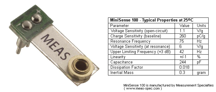
Figure 1 - MiniSense 100 Piezo Accelerometer/ g-Sensor
The sensor shown above has a capacitance of only 244pF, so to get response down to 1Hz you need to use a 1GΩ input bias resistor. You can buy 1GΩ resistors (1,000Meg) for less than $2.00 (at the time of writing) but the amplifier itself must have a very high input impedance and extremely low input current, or it will load the sensor and you won't get any useful output at low frequencies. If an input stage has an input current of just 0.1uA, that creates (or attempts to create) a voltage of 100V across a 1GΩ resistor, so you must use a device with less than 1nA (1V across 1GΩ) input current. Many FET input opamps are specified for input bias currents in the pA (pico-amp) range. 65pA is typical for a TL072 for example, and that will cause an input offset of 65mV.
Bipolar transistors are not really useful because it's extremely difficult to keep the input current low enough, although it is possible to use them with careful design. The design effort isn't worthwhile though, because there are much easier ways to get sub 1nA input currents. A FET (or small-signal MOSFET) needs almost no input current at all and the design is a great deal easier. However, it may not be that simple, because all active devices have some input capacitance, and that needs to be considered as well.
There is another common circuit that's used with capacitive sensors, and that's called a charge amplifier. When used with low capacitance sensors they typically need an extremely high resistance, and the resistance is increased further if gain is needed. I don't intend to cover charge amps here because they are a rather specialised case, and don't have many particularly desirable features compared to more conventional techniques (especially if you need gain from the input amplifier). However, a charge amp is not affected by the cable or other stray capacitance because its input is a very low impedance. They are certainly interesting, but are harder to implement that the circuits described. There's plenty of information available for anyone who wants to build a charge amplifier, and a web search will provide many examples.
This article discusses the various options that can be used, and the circuit shown in Figure 9 is the only one that should be constructed if you need a nigh-impedance test amplifier. Feel free to experiment though, as that's the great joy of DIY electronics. There's always more that you can learn, and the ideas covered here are interesting to play with.
The final circuit (Figure 11) is different - it's a 'charge amplifier', which has the distinct advantage of having a very low input impedance. While not useful as a general-purpose test amplifier, if you do need to condition the output of a piezo transducer, a charge amp offers a significant advantage. Because of the low input impedance, it's immune from cable capacitance and, more importantly (and usefully) it picks up almost no hum!
Noise is potential problem - high impedances cause thermal noise in resistors that can be well above the level you are trying to amplify. See Noise In Audio Amplifiers for more info about noise, how it's measured and calculated. Voltage noise is worked out by ...
VR = √ ( 4k × T × R × f )
Where ...
VR = resistor's noise voltage
k = Boltzmann's constant (1.38E-23)
T = Absolute temperature (Kelvin)
R = Resistance in ohms
f = Noise bandwidth in Hertz
In high impedance circuits, noise current becomes the dominant problem.
IR = √ ( 4k × T × f / R )
Where IR = resistor's noise current
Noise voltage and current can be worked out so you know just how much noise will be created just by the input resistor. A 1GΩ resistor has a noise voltage of 57µV at 27°C (roughly 4µV√Hz), and the noise current is 57pA (you can also use Ohm's law to determine current from voltage or vice versa). Other noise sources include 1/f ('flicker' noise) and 'shot' noise, both of which are developed in active devices. This article is not going to attempt to cover extremely low noise applications, because they invariably require exotic parts that may be difficult to obtain. Instead, a 'utility' amplifier will be the end result, one that will satisfy most common requirements.
High impedance solutions that may initially seem perfectly reasonable can have some very unexpected consequences, so it's essential to understand the various methods that can be used, and how they react in a real circuit. In general, JFETs (junction field effect transistors) are suitable for high impedance applications, but you have to choose the device carefully. Small signal MOSFETs can also be used (e.g. 2N7000), but they are usually much noisier than JFETs and may also have a higher input capacitance. That requires 'interesting' additional circuitry to get the full frequency range.
When FETs or MOSFETs are used, they will generally be connected as simple source followers. This helps to reduce the effects of input capacitance, but with no gain there is a noise penalty because the first stage of any amplifier generally determines its noise figure. Using JFETs in a cascode connection provides gain without any effective increase in the input capacitance, but that is highly dependent on the FET characteristics. Common FETs have an extremely wide parameter spread with standard production devices, making the design a challenge. Unless there's a good reason not to do so, consider using a FET input opamp, as this makes everything far more predictable.
However, the noise level from common FET input opamps is usually fairly high, and this has to be considered. Depending on the level you need to amplify, you may find that noise is intrusive, but piezo sensors are capacitive and their capacitance helps to roll off the noise above the frequency determined by the input resistor and the sensor's capacitance (which includes the capacitance of the cable between the sensor and amplifier.
Hum (50 or 60Hz) is a real problem, and all high impedance circuits are very sensitive to electrostatic hum fields. Without shielding, you'll almost certainly find that the hum picked up is far greater then the signal. The capacitance of the sensor (and cable) helps again, because it will roll off hum just as well as it will resistor and opamp noise. The entire circuit needs to be in an earthed metal case, and ideally so does the sensor itself.
Hum loops will not be created provided there is no secondary electrical connection between the sensor housing and the preamp. If the sensor is to be buried, consider using an outer plastic housing so that the sensor's shield doesn't make direct contact with damp soil or other conductive materials. You can use a plastic case and line it with aluminium or copper foil if you prefer.
The term "bootstrap" is applied to several completely different circuit topologies, and they are not equivalent. I've shown a bootstrapped current source in many of the audio amplifiers shown on the ESP site, and a different form of bootstrapping is used in many 'high-side' MOSFET driver ICs. As used here, the term applies to input stages, where the bootstrap circuit is used to increase the apparent value of a bias resistor.
The concept of bootstrapped input stages is both well known and commonly applied, and the Designing With Opamps series shows a basic bootstrapped input stage intended to obtain a very high input impedance (albeit in its most simplistic form). While the use of a bootstrap circuit seems very appealing at first glance, there are several problems that aren't immediately apparent, and are rarely discussed.
A bootstrapped input circuit uses positive feedback to make the input bias resistor 'disappear'. The general scheme is shown below, and I've assumed an input capacitance of 250pF, as may be typical of a low capacitance piezo sensor like that shown in Figure 1. If we want the low frequency limit to be no greater than 10Hz, the impedance seen by the sensor can be no less than ...
Z = 1 / ( 2π × 250p × 20 )
Z = 637 Megohms
This is such a high resistance that it requires special techniques to achieve it. It's not just the bias resistor that has to be considered, but the input impedance of the amplifying stage has to be such that it doesn't reduce the impedance. The general 'rule of thumb' is that the amplifier stage should have an input impedance of not less than 10 times the bias resistor - 6GΩ is required.
A higher impedance won't hurt at all, and you might consider using a TL072 or LF353 opamp (Zin of 1TΩ for both). In reality, response is usually expected to 1Hz, but many piezo sensors have more than 250pF of capacitance (some being a great deal higher). The following examples will be based on a 250pF sensor for convenience. In the circuit below, the bootstrapping (via C1) boosts the input impedance to about 240MΩ, which isn't good enough to get 1Hz from a 250pF sensor. If you need lowest possible noise, the OPA627 is one suggestion (although it's very expensive) - there are others and wide price variations.
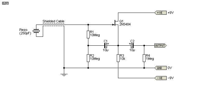
Figure 2 - High Impedance Preamp With Bootstrapped JFET Input Stage
Using a bootstrap circuit certainly achieves the high impedance required, but what can't be seen in a frequency-domain measurement is what happens to the frequency response. At a low frequency (determined by the capacitance of the source and the bootstrap capacitor) there can be a large response peak. The source capacitance includes cable capacitance and all stray capacitance, including the input capacitance of the FET or opamp used.
This has two side-effects, neither of which is desirable ...
The hidden issue that is rarely mentioned whenever bootstrapped input stages are discussed is the high Q filter. The source capacitance and bootstrap capacitor form a filter that will have a high Q unless it's understood and accounted for. This becomes a problem if different sensors (or cables) are used, because as the source capacitance changes, so do the characteristics of the filter formed by the bootstrap connection. The filter is not easy to see in the stage shown above, but you will know it's there when you see the response rolls off at 12dB/ octave, not 6dB/ octave as you may have expected.
Note that the 12dB/ octave rolloff doesn't apply to the Figure 2 circuit because the 10µF cap (C1) is much larger than needed, and over the visible response curve it's only 6dB/ octave. It changes to 12dB/ octave at around 50mHz which is almost impossible to measure, but is easily simulated. Depending on the JFET you use, C1 and C2 may need to be reversed.
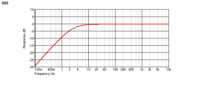
Figure 3 - Bootstrapped Input Stage Response
The high Q filter issue generally doesn't arise if you use a FET source follower by itself as shown in Figure 2, because its gain is considerably less than unity. That helps to prevent a high-Q filter from being formed, but also limits the impedance that can be achieved. For example, if the gain is 0.95 that means that only 95% of the input voltage is reflected by the bootstrap circuit, so the effective impedance of the input resistor is lower than expected but it has no 'bad' habits.
As an example, we'll use a 10MΩ resistor and a JFET as shown in Figure 2. Let the instantaneous input voltage be 1V, and the output voltage 950mV (a gain of 0.95, which is actually a loss). The voltage across the input resistor is 50mV (1V - 950mV), so its impedance appears to be 200MΩ ...
Vin = 1V
Vout = 0.95V
VR1 = Vin - Vout = 50mV
R1(apparent) = 10M × ( 1 / 50m ) = 200M
However, it's important to understand that the exact same circuit using a 2N7000 small-signal MOSFET has a gain of 0.993 and it will create a large peak in the response unless C1 is made much larger (at least 100µF). The gain of a MOSFET used as a source follower is temperature dependent, so caution is advised to ensure that no peak is generated if the gain should increase. If a higher capacitance sensor is used in place of the design value, the peak comes back again, but at a lower frequency. An opamp is even worse, as described below ...
When an opamp is used as a voltage follower, the gain is much closer to unity. This means that there's almost no voltage at all across R1, and its impedance is raised by a factor of perhaps 1,000 or more and it virtually disappears. The gain is so high that it's essential to include a resistor to prevent extremely high gain at some low frequency. This extra resistor is shown in Figure 3, and without it there's a pronounced peak at 0.68Hz. As simulated using a TL072 opamp and a 250pF source, with R3 set for zero ohms there is a peak of almost 37dB. The circuit will be unstable, and you may never know why if you are unaware of this peculiar problem.
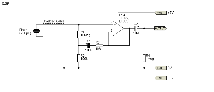
Figure 4 - Bootstrapped Input Using An Opamp
An opamp based bootstrap circuit is shown above, including the resistor (R3) added to reduce the amount of positive feedback. Without the resistance, instability is probable and you may find that you've built a low frequency oscillator instead of an amplifier. If it does just amplify, it will take some time to settle after power is applied - A test version that I built took over 60 seconds before it was stable, and that included R3. Note that there is no reason that R1 and R2 must be equal. That's merely an expectation, but as shown above (and below) it makes little difference provided C1 is sized appropriately.
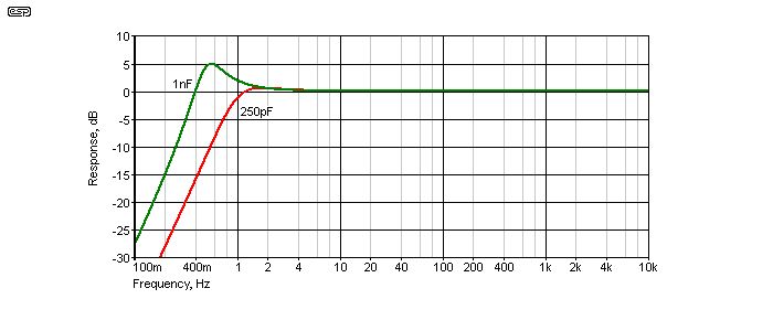
Figure 5 - Low Frequency Peak Caused By Bootstrapping
The size and frequency of the peak both change with different source capacitance and source resistance, and the graph shows the response with a 250pF sensor (red) and a 1nF sensor (green). Most capacitive sensors have a low ESR (equivalent series resistance), so there's nothing to mitigate the peak. Adding R3 as designed (1.8k), input impedance is over 650MΩ and there's (almost) no peak at all ... until the source capacitance changes. As noted earlier, this may simply be because you use a different cable. If the 'new' capacitance is 500pF, there's a 2.6dB peak at 0.86Hz, and a 1,000pF (1nF) source causes a peak of 5dB at 0.54Hz.
This is one of the biggest problems with the bootstrap circuit - there is interaction between the preamp and its source, and it will behave differently depending on the source resistance and capacitance. You can improve matters a little by increasing the value of the bootstrap capacitor, but that really only moves the problem to a lower frequency. You may not be able to measure it, but it's certainly there. For many applications this is unacceptable. Provided the sensor, cable and bootstrapped preamp are designed as one there will be no issues, but that can be very limiting.
There's another problem that's hiding as well - noise. The bootstrapped resistance is 10MΩ as shown, and the broad band voltage noise from the resistor alone will be about 58µV, calculated from the formula shown above. The resistor and source capacitance form a low pass filter, so we can work out the -3dB frequency of 250pF and 10MΩ - 63Hz. That means that if you want to measure anything below 64Hz, you'll get nearly all the noise with only high frequency noise filtered out. Typical piezo geophones are useful between 1Hz and around 40Hz, so you'll get the majority of the resistor noise along with the signal.
The above is not to say that you shouldn't use a bootstrap circuit, because they are inherently useful. If you only desire a modest impedance boost (no more than 10 times), you can use a 10MΩ resistor to obtain an input impedance of 100MΩ easily. While it's still possible to get an unwanted response peak, it's far less likely, and the amplitude will be within acceptable limits for a wide range of sensor capacitance. To get a ten-fold (near enough) increase of the value of R1 in Figure 4, simply make R3 one tenth the value of R2. The maximum bootstrap voltage is 0.909 (referred to the input voltage), so R1 appears to be 11 times its real value. Then again, 100MΩ resistors are readily available and inexpensive, resulting in a simpler circuit.
You can get 1GΩ resistors fairly easily, and they shouldn't break the bank. You don't need very high voltage types (they can be seriously expensive), and the ones I used for testing cost less than AU$2.00 each. This is a very simplistic approach, but this really is an application where simplicity gives the most consistent results. Obviously the opamp (or FET) needs to be carefully selected for the task, but this should not be a problem.
There are many benefits to using a high resistance, and simplicity is but one. The circuit is inherently well behaved, and does nothing that can come as a surprise. When power is applied, it settles almost instantly and is ready for use, and the low frequency rolloff is absolutely predictable, being based only on the sensor's capacitance and input bias resistor value used. If a calculation is done for noise, broad band noise (up to 20kHz) looks pretty bad - 575µV is rather a lot of noise signal. However, all is not what it may seem.
The use of a high resistance has a hidden benefit. Even with the hypothetical 250pF sensor that's been assumed here, the noise will be rolled off above 0.64Hz, since the input resistor and sensor capacitance form a low pass filter. It's not a wonderful filter by any means, but the majority of the noise from R1 will not cause any issues.
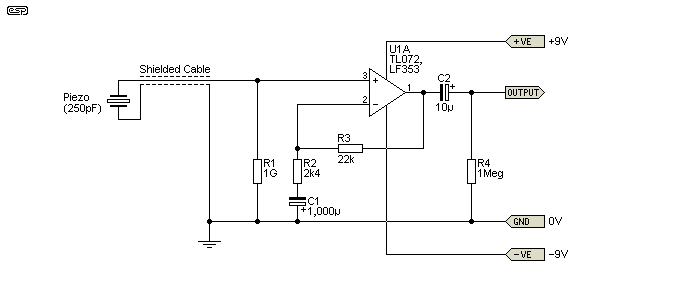
Figure 6 - High Impedance Preamp using 1GΩ Resistor
The circuit is completely conventional, but note the polarity of the electrolytic capacitors. I used a TL072 for testing, and the output will be negative (by around 60-100mV) with a 1GΩ input resistor. Since I included a gain of 10 (close enough), that would become -0.6 to -1V if the feedback path used DC coupling. A 1,000µF cap allows response to 6.6mHz (0.0066Hz), well below the frequency set by the sensor and R1 (0.64Hz for a 250pF sensor). The gain can be increased by reducing the value of R2, and the 1,000µF cap used for C1 allows for a gain of up to 100 (R2 = 2.4k), with a -3dB frequency of 0.066Hz.
It's worth noting that all capacitor ('condenser') microphones use high value resistors. I've not seen one schematic that shows a bootstrapped input stage. The resistance you use will depend on the capacitance of the sensor and the minimum frequency needed. The sensor shown in Figure 1 has a capacitance of around 250pF (actually 244pF), and if you need to get down to 1Hz then you need a 1GΩ resistor. Other sensors can have a great deal more capacitance - a simple piezo disc can have a capacitance of over 10nF, so the resistance needed is much less. Somewhere around 20MΩ is fine, and that gets to 0.8Hz (-3dB). A pair of 10MΩ resistors in series will be fine for a 10nF sensor, and no special construction techniques are necessary because of the comparatively low resistance. Not that 20MΩ is low, but compared to 1GΩ it is  .
.
With any very high impedance circuit, even small traces of contaminants will cause leakage that reduces the input impedance. One technique that's often used is a 'guard track' that surrounds the input components and is held at the same potential - bootstrapping again. This is fine for production, but for one-off or small quantities where a PCB isn't warranted, it's almost impossible to achieve. No special precautions are needed or necessary with bias resistors of 10-20MΩ, but they are essential with the 1GΩ input stage.
The alternate method is to 'sky-hook' the input components - literally joining them in mid-air. If the FET gate pin or opamp's non-inverting input pin is bent up so it doesn't pass through the prototype board, the input resistor, protection diodes and input lead are simply soldered to the 'floating' pin with no contact to anything else. After soldering, the solder joint and FET (or opamp) must be thoroughly cleaned so there is no trace of flux or skin oils on the insulating surfaces.
If you can get PTFE (Teflon) stand-off insulators you can use one of them to support the connections, but if you sky-hook carefully there should be no need for additional support. Needless to say, if you intend to attach a heavy coaxial cable to the device pin then you will need some extra reinforcement or the cable will eventually break off the FET or opamp pin when it's moved around.
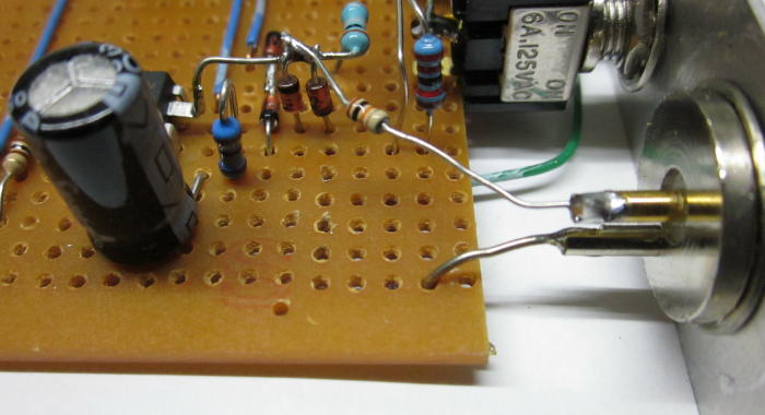
Figure 7 - Photo Of Sky-Hooked Input Stage
You can see how the input parts are mounted in the photo. Everything that runs at the maximum input impedance of 1GΩ is separated from the Veroboard type PCB. The input current limiting resistor (R1) is mounted in mid-air from the connector. If there is a greater distance than allowed by the resistor leads, the resistor and added wire should be protected with heatshrink tubing and kept away from other parts of the circuit and the case. When you have an impedance of 1GΩ, every precaution has to be taken against leakage.
High capacitance sensors (> 10nF) are much easier to deal with, because the resistance is so much lower. Normal prototype techniques will usually be quite ok when the bias resistor is no more than 20MΩ, but it's still necessary to ensure that the board is thoroughly cleaned after soldering. Many types of flux become conductive if they absorb any moisture, and that may alter the performance of the circuit.
Not shown in the photo above is an electrostatic shield that separates the high impedance input from the output. Even though the output is some distance from the input, at high gains the preamp will oscillate because the input impedance is so high that it can pick up some of the output from nearly 20mm away. Expecting perfect behaviour is simply not possible, because the circuit is so sensitive that it's hard to use it with an open circuit input (which isn't useful anyway). I built mine to have gain switchable from x1, x10 and x100, and at the highest gain it's now stable after I added the shield.
This is another can of worms. I tested some 1N4148 diodes to measure their leakage and determine their effective resistance. With 15V across a reverse-biased diode, I measured a current of 1nA. Normally we wouldn't be at all concerned with such a low current, but if the equivalent resistance of the diode is worked out based on the current measured, you get 15GΩ, so the traditional pair of protection diodes will have a combined impedance of 7.5GΩ. This reduces the input impedance and introduces temperature dependence, because the diode resistance is in parallel with the input impedance.
I tested this, and was able to bias the input of a TL072 opamp using only a pair of 1N4148 diodes. The bias level was unstable because the diodes leakage depends on temperature, and no two diodes will ever be equal. It's quite obvious that using diodes in the conventional way to protect the gate of a FET is not going to work very well.
You may well ask how I was able to measure such a low current without the use of very specialised test equipment. That's easy - I used a 5 digit bench voltmeter with an input impedance of 10MΩ in series with the diode and a 15V DC supply. The meter measured 0.01V, so the current is equal to 0.01V / 10M, or 1nA. The diode passed 1nA with 15V across it, so its leakage resistance is therefore 15V / 1nA = 15GΩ. (Note that this is highly temperature dependent, and the rated leakage current of a 1N4148 is 25nA at 25°C with a reverse voltage of 20V.)
Fortunately, this is an area where using a bootstrap circuit will not cause a problem, so instead of bootstrapping the input resistors, we can bootstrap the protection diodes. Under normal operating conditions, the diodes will have very close to zero volts across them, so they can no longer cause a problem. The protection scheme is shown below.
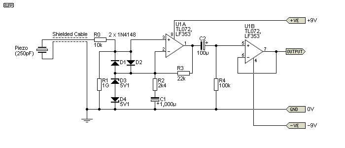
Figure 8 - High Impedance Preamp With Protection Diodes And Output Buffer
R0 has been added to limit the worst case input current. D1 and D2 are bootstrapped from the feedback network, but that's perfectly alright because the voltages at pins 2 and 3 are almost identical. D3 and D4 will not cause distortion, because the signal voltage across them can never be high enough for them to conduct, but input spikes over ±5.7V will be clipped. The values of R2 and R3 give the circuit a gain of 10 (20dB), and the gain can be raised or lowered by varying R2 (don't reduce it below 2.2k or C1 will cause premature low frequency rolloff) ...
Gain = R3 / R2 + 1
Gain = 220k / 24k + 1 = 10.16 (20.14dB)
The circuit shown has been tested, and performs exactly as expected. The DC offset caused by the TL072's minute input current is about -100mV, and the final DC blocking capacitor is necessary. Needless to say, the extremely high input impedance means that hum and/or other noise is picked up very easily, and the small sensor capacitance does little to reduce the 50/60Hz noise. Accordingly, the entire circuit must be in a fully shielded enclosure.
The complete schematic is shown below. It includes a buffer stage followed by an optional low pass filter (R6 and C3) that's been included to remove frequencies outside the range of interest. As shown it has a -3dB frequency of 21kHz (3.3nF) or 72Hz (1µF), but this can be changed to suit your needs. If the output is delivered directly to a PIC microcontroller or an analogue to digital converter (ADC), you may need to bias the output to +2.5V (assuming a 5V supply) so the ADC's input is centred. You need to determine whether the DC offset is needed from the datasheet for your digitiser.
The additional bias resistor is shown marked with '*', and it connects to the ADC's supply voltage (typically 5V or 3.3V). The DC blocking capacitor (C2) is required whether you apply a DC offset or not, because there will be some offset from the first opamp (U1A) when a 1GΩ input resistor is used. The -3dB frequency with the 100µF cap shown is 0.016Hz without the DC offset or 0.032Hz if it's included. No additional filtering is needed because C2 will filter out any noise from the 5V supply. The low pass filter (R6, C3) gives an upper -3dB frequency of 21kHz (3.3nF) or 72Hz (1µF), and C3 can be omitted if no HF rolloff is needed. R6 can then be reduced to 100 ohms.
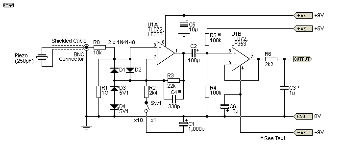
Figure 9 - Complete High Impedance Preamp
A switch is included to allow the gain to be switched from x1 to x10. When the switch is open, the opamp has full feedback and operates as a buffer. When closed, R2 is in circuit and increases the gain to x10. This is optional. Feel free to add another switch and resistor that can also be switched into circuit, increasing the gain to x100 (resistor values must be changed - see below). If both switches are closed the gain will be x102 (close enough).
The power supply depends on your application for the circuit. For intermittent use, a pair of 9V batteries will be perfect, but if the circuit needs to be powered continuously you will need to use either a battery pack with a 'smart' charger or a mains supply. The latter will need to be a linear supply in most cases, because switchmode plug-pack (wall wart) supplies are generally too noisy. Supply bypass capacitors are essential, and although I've shown 10µF (C4 and C5), you can use higher values if preferred. Adding parallel 100nF ceramic caps is not necessary with the TL072 or LF353, but they do no harm and can be included if you wish.
C4 is not optional if you have a switched gain of ×1 and ×10 (or ×100). It will reduce noise (and signal) above 20kHz with 330pF at a gain of 10. It can be increased if you include the output filter - you can use up to 100nF if the circuit is only to be used for low frequency measurements. For example, if you use the 1µF output cap (C3) and 39nF for C6, the upper -3dB frequency is 67Hz, with a 12dB/ octave rolloff. There will be some (unwanted) high frequency boost caused by the capacitance of the two zener diodes when the circuit is operated with a gain of unity or x10, and that is partly mitigated by including C4.
If you wish to use a single supply (12-18V for example), add a 1k resistor from each incoming supply to the common earth/ ground terminal, and increase C4 and C5 to at least 100µF. Because overall current drain is quite low, this simple voltage divider arrangement will work perfectly.
While the schematic shows the circuit with a switchable gain of ×1 (0dB) or ×10 (20dB), my prototype has gain that's switchable to ×1, ×11 and ×101. R3 is 100k, and I used 10k and 1k resistors for the R2 feedback resistor, with series switches to C1. With C2 at 1,000µF as shown, the response extends to 159mHz with 1k for R2, so low frequencies are not compromised. Remember to include C4!
While the circuit will happily provide a signal to a PC sound card, none has the low frequency response needed for measuring low frequency noise or vibration. It's expected that anyone building the circuit will already have decided on the method of recording or logging the output, and it's only the analogue part that causes any problems. This is now common, as many people have mastered the art of programming microcontrollers and capturing the data to a memory stick or PC hard drive. The analogue side of electronics is often considered deeply mysterious, and countless forum posts show that this is a real problem.
R1 will usually be selected based on the sensor you are using. With high capacitance sensors you will probably only need somewhere between 20MΩ and 100MΩ, with 1GΩ as shown only necessary for sensors with a capacitance below 1nF (1,000pF). A 10nF sensor with a 1GΩ load has a theoretical lower limit of 0.16Hz, and it will be very sensitive to thermal effects. Pyroelectric properties come free with most piezo ceramic materials, so a stable operating temperature is essential.
One way to make the preamp as 'universal' as possible is to build it with an input impedance of 1GΩ, and if you have other sensors you simply add the appropriate loading resistor directly in parallel with the sensor itself. This provides the maximum flexibility. For example, if you have a 15nF sensor that is intended to get down to 1Hz, simply wire a 10MΩ resistor in the same (shielded) box as the sensor, with the resistor in parallel with the sensor itself.
Experimentation is the key to getting the results you need from the sensors you want to use.
If you need a maximum gain of 100, you need to increase the feedback resistors by a factor of 5, so R3 will be 100k and R2 (x10) will be 11k, and R2 (×100) will be 1k. That arrangement is more sensitive to stray capacitance, and C4 has to be reduced to around 68pF. You can keep R3 as 22k, but then C1 will cause low frequency rolloff when R2 is only 240 ohms (gain of 100). There are many options of course - unity gain with perfect flatness is guaranteed if you use a switch to short R3, but beware of stray capacitance from the switch and its wiring to the input. It will prove almost impossible to minimise coupling between the two, which will cause instability (oscillation) with a gain of 100.
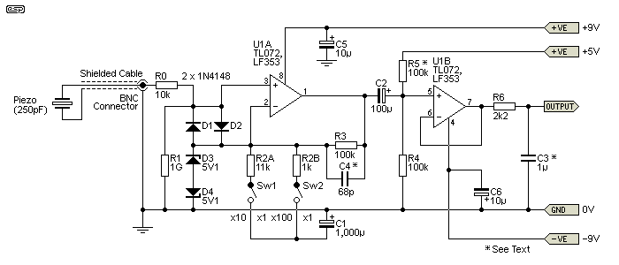
Figure 10 - Complete High Impedance Preamp With x1, x10 & x100 Gain
The version above shows the changes for a preamp with switchable gain up to ×100. Although shown with two SPST toggle switches, you can use a 'centre-off' toggle if you can find one with two latching 'on' positions, one either side of centre. These are commonly known as on-off-on. You can't use a switch where one or both positions off-centre are momentary. Capacitive coupling between the input and output must be minimised, and an electrostatic shield will be needed around the (sky hooked) input section. I have to leave this to the constructor, because it depends on the physical layout used.
Frequency response is ok - it's good for around 13kHz with a gain of 100, increasing to 23kHz with a gain of 10, but there is a high frequency rise on the x1 setting because C4 can't compete with the zener diodes capacitance plus any stray capacitance from the Veroboard. This is unlikely to be a problem in real life, because most accelerometers and other piezo transducers don't have useful output at high frequencies. Consequently, you might decide to make C4 larger than 68pF, restricting the high frequency response. I'll leave this to those who build the circuit.
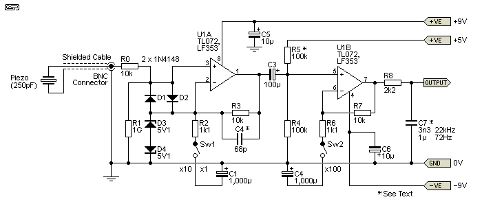
Figure 10A - Alternate High Impedance Preamp With x1, x10 & x100 Gain
The drawing above shows another way to increase the gain, that also maximises the audio bandwidth. Each stage can be operated at a gain of unity or x10, and with both set for x10, the gain is 100 (actually 101.83 if we take it to the letter). You don't have to use 1.1k resistors (R2, R6), and with 1k the gain will be x11 or x121. This will rarely be a problem, as this isn't intended to be a precision test set. Resistor tolerance (1% metal film types are recommended) will have a small effect as well. Perfect x10 and x100 is possible, using 27k and 3k resistors for each feedback network.
From a document titled 'Bob Pease Lab Notes' (1989-1990) [ 8 ] there's a high impedance probe that's fairly specialised, but may come in handy. Unfortunately, the JFETs used are no longer available (2N5486 or 2N5485), and a simulation using J113 FETs gave roughly equivalent results. While the original info claims input impedance of 1011Ω (100GΩ), this appears only to hold true at low frequencies, below 1Hz. I'm unable to test the claim, but simulation shows that Zin falls with increasing frequency. The simulator shows impedance to be above 100GΩ at frequencies below 2Hz. It was claimed that bandwidth extended to 90MHz, and while probably true, the simulated input impedance showed 10MΩ at 1MHz. The full bandwidth can't be realised unless the source impedance is low (6kΩ or less).
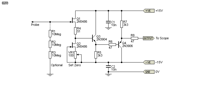
Figure 11 - Ultra-High Impedance Circuit (Bob Pease)
The circuit is shown exactly as Bob Pease published it, with the exception of R8 which prevents possible oscillation if the emitter-follower has a capacitive load. There is zero input protection, and the input signal must never exceed the ±15V supplies. While 3 × 10MΩ resistors are shown in series as an option, there's no reason that you can't use a 100MΩ or even 1GΩ resistor instead. Input capacitance is claimed to be 0.29pF, and in theory that would result in a -3dB frequency of 548Hz with a 1GΩ source impedance.
From the original document, it's hard to know exactly what Bob's intentions for the circuit were. He stated that it was optimised for input impedance and not frequency response, and unfortunately I don't know if the simulator is telling naughty fibs about the response with a high source impedance. It's more than likely telling the truth, because I've run enough simulations to know when the results are completely unexpected (and likely wrong). The results I obtained seem ... plausible.
Charge amplifiers are less common than high impedance circuits, and aren't suitable for a general-purpose high impedance bench amplifier (for example). While this article describes high impedance inputs, a change amp has a very low input impedance. The capacitance of the transducer and feedback cap (Cf) determine the gain. If Cf is smaller than the piezo capacitance, the circuit has gain (by the ratio of the two capacitances). Making Cf larger than the piezo capacitance makes the gain less than unity, but it can accommodate much higher input levels.
If you need to 'condition' the output of any capacitive sensor (including piezo types), a charge amp offers the unique advantage that hum pickup is almost eliminated. It's also insensitive to cable capacitance, so a high capacitance cable won't attenuate the signal - however, it will increase the opamp's noise output. In the drawing below, the charge amp itself is based on U1A, and has unity gain if the piezo has a capacitance of 250pF. If the piezo has more capacitance, Cf can be increased in value (ideally the same as the piezo), and Rf can be reduced. For example, with a 10nF piezo and 10nF for Cf, the gain remains at unity and Rf can be reduced to 2.5MΩ for the same -3dB frequency (6.4Hz).
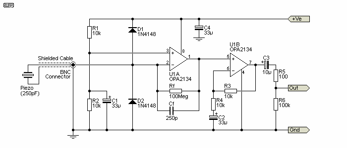
Figure 12 - Charge Amplifier, 6dB Gain
If the charge amp is configured for unity gain (which is the ideal) but more gain is needed, it's added with the second stage. With the values shown for R3 and R4, gain is 6dB, but it can be changed as required. Purely as an example, the circuit is shown using a single supply (which can be anything from 5V to 30V with the OPA2134 shown), or a split supply can be used.
This circuit has been included simply because it's very common with accelerometers and many other scientific/ industrial sensor systems. Because it doesn't have high input impedance it is a little out-of-place, but not including it would limit your options. The low input impedance makes it almost immune from hum, something that will always be a problem with 'true' high-Z preamps (and I know this from personal experience).
Most of the salient points about construction have already been covered. As already noted, the non-inverting input pin of the TL072 opamp (pin 3 as shown) must be lifted so it's not inserted through the Veroboard, and resistors R1 and R2 connect directly to the IC pin, along with D1 and D2.
The remainder of the circuit is not at all critical, but you will need a very well shielded enclosure to minimise 50/60Hz hum. The output buffer is optional, as is the low pass filter shown. If you are using a piezo sensor as a geophone (for example), most of the interesting signals will be below 20Hz, with some being a great deal lower (0.1Hz is easily achieved with a reasonably high capacitance sensor).
I suggest a BNC connector for the input, because I've tested a sample of a few I have to hand, and their insulation resistance is too high to measure. You also have to be careful with the cable used to the sensor, as it also needs extremely high insulation resistance or low frequency performance will be impaired. RG174/U is one suggestion, as it's small (less than 3mm diameter), and has acceptably low capacitance at around 100pF/ metre. It also seems to have fairly low triboelectric noise. Keep the cable as short as possible.
The cable's capacitance has two side-effects. The first is that it reduces the output level from the sensor, because it forms a capacitive voltage divider. If the sensor has a capacitance of (say) 100pF and the cable has the same, the level will be reduced by 6dB.
The second effect actually works in our favour. Because the cable and sensor are in parallel, the effective capacitance is the sum of the sensor's and cable's capacitance, so using the same values as before, the total capacitance is now 200pF, and the -3dB frequency is moved lower by one octave. Where the low frequency -3dB frequency would normally be 1.6Hz, the cable capacitance moves that down to 0.8Hz (assuming a 1GΩ resistor).
However, be aware that as the cable is moved it will generate a voltage (triboelectric noise) that cannot be distinguished from that from the sensor, so everything needs to be kept very still while a measurement is being made. The amount of signal generated by the cable depends on the dielectric used, and some cables will be a lot more sensitive than others. I haven't tested a range of cables and can't make a specific recommendation based on self-noise, but a coax cable using a foam polyethylene dielectric with copper wire would be a safe choice. I use RG174/U cable quite a bit, and it seems to have fairly low triboelectric noise from the limited tests I've done.
When the circuit is built, I suggest that you measure the DC offset from the input opamp before soldering in C3 (electrolytic capacitor). You will need to use a capacitor from the input to ground, or a measurement will be impossible due to 50/60Hz hum pickup. Depending on the input resistance you may see either a positive or negative DC voltage at the output of U1A, but it will typically no more than 100mV. I measured -100mV with a 1GΩ resistor, but +20mV with 20MΩ input resistance. While electros aren't bothered by small reverse DC voltage (< 1V), it's not hard to measure the voltage on pin 1 and orient the capacitor so its polarity is correct. You may need to do the same for C2 if you won't be using the 2.5V DC offset feature, because it can be reversed as well. If the 2.5V DC offset is used, C2 must be oriented as shown above.
No special precautions are required with the charge amplifier, unless the feedback capacitance is very small and the feedback resistor is a high value (> 10MΩ). If that's the case, you need to take the same precautions described above, namely using 'sky hook' techniques to minimise leakage across the resistor. You will also need to use a capacitor with particularly good insulation, or that will compromise performance.
As stated earlier, this project is not (and is not intended to be) the be-all and end-all of high impedance preamplifiers. It's designed to be cheap, easy to build, and for general experimentation. The fact that it works very well is a bonus . I built mine to have a maximum gain of 100, and once I fitted an internal screen to protect the input, I was finally able to run it with no source connected.
To give you an idea of how sensitive a 1GΩ input stage can be, I found that I could measure 50Hz hum that was picked up by the inner terminal of the BNC connector. The only way to eliminate the hum completely was to press a piece of metal across the front of the connector to shield it from the outside world. A tiny 1mm diameter pin socket recessed inside the earthed BNC connector was enough to pick up several millivolts of hum - I would never have believed it if I hadn't seen it for myself.
Mine also has no high frequency rolloff built in, because its purpose at this stage is not exactly undefined, but I wanted it to be flexible. As a result, a noise test with the input open-circuit shows it to be ... abysmal! This is to be expected of course, because the TL072 isn't the quietest around, but most of the noise is due to the 1GΩ resistor. The resistor alone contributes 575µV, so with a gain of 10 that becomes 5.75mV, and a gain of 100 yields 57mV. Yes, 57mV of noise, and this has been (more or less) confirmed by measurement. The measured noise with a gain of 100 was actually 45mV on average, and listening to it proved it to be wide band white noise.
However, as soon as a piezo sensor is connected, the noise level falls dramatically, depending on the capacitance of the sensor. This happens because the sensor (and cable) capacitance filters all but the lowest noise frequencies at 6dB/ octave, with the -3dB frequency determined by the total capacitance.
All in all, if you have a need to measure signals at very high impedance levels, this is another very useful tool for your arsenal. The cost is moderate, and it's probable that the case and connectors will cost far more than the circuit itself.
Some of the material presented here has been prepared based on information gathered from the Net, but the majority is based on experimental data, simulations and bench testing. The references below will be of assistance to those who want more information.
Main Index
Articles Index
| Copyright Notice. This material, including but not limited to all text and diagrams, is the intellectual property of Rod Elliott, and is © 2015. Reproduction or re-publication by any means whatsoever, whether electronic, mechanical or electro-mechanical, is strictly prohibited under International Copyright laws. The author (Rod Elliott) grants the reader the right to use this information for personal use only, and further allows that one (1) copy may be made for reference. Commercial use in whole or in part is prohibited without express written authorisation from Rod Elliott. |