
|
| Elliott Sound Products | Power Amplifier Development |
 Main Index Articles Index Main Index Articles Index |
Since the very first power amplifiers were developed in the 1920s, there have been countless different designs. The primary goals were usually to get more power with less distortion, and this quest continues. Early amps were very low power, and were paired with highly sensitive speakers, often using horn loading to get more 'noise' with the limited power available. Single-ended triode amplifiers were initially the only option, until design skills improved and new designs were developed. Most of these early single-ended amps would struggle to get even 5W output, using large power triodes. Push-pull operation could increase output by a factor of at least four.
Initially, valves were used primarily for radio/ 'wireless' detection and amplification, along with telecommunications (the latter has been a primary 'driver' of electronics development until fairly recently). Once people realised that it was possible to amplify weak signals to drive a loudspeaker (especially for wireless, public address and 'talking' movies from 1927 onwards), the race was on to get more power. It was quickly discovered that push-pull was superior to single-ended operation in all respects. Early valve amplifiers used triodes, because they had nothing else until the pentode was invented in 1930, with the beam-tetrode following not far behind (to avoid the patents held by Philips). 'True' tetrodes had a limited production, because they didn't work very well (hence the pentode).
With the advent of the transistor in 1948 there was a whole new design process to master once transistors became commercially available. By the 1970s, most development of valve amplifiers had ceased, since the 'writing was on the wall'. Some of the early transistor designs were very poor by modern standards, but some compared favourably against 'equivalent' valve circuitry. That's not to say that they were markedly 'better' than an equivalent valve power amp, and many people complained that they were inferior for a variety of reasons.
Not all of the complaints were justified, but there's no doubt at all that many were more than justified. Depending on the texts you read, some of the issues were purely subjective, because many people didn't (and some still don't) trust that transistors could achieve good results. Some differences resulted from the much lower output impedance of transistor amps. This came about for two reasons ... most valve amps had limited feedback because phase shift in the output transformer could cause the amp to oscillate if the feedback ratio was too high. Coupled with the high output impedance of valves (determined mainly by the internal plate resistance), these amps allowed the loudspeakers of the day to 'do their own thing' to an extent. With a typical damping factor of somewhere between unity and ten, the speaker would produce more bass and often more treble as well. The bass would often tend to be somewhat 'boomy', because Thiele-Small parameters were way off in the future, so enclosure designs were often empirical, and 'optimised' with common power amplifiers of the era.
Transistors changed this. Not only is their output impedance much lower than valves, but they also (generally) have higher gain. This meant that more feedback could be used, reducing both distortion and output impedance. If used with a speaker designed for a Mullard 5-10 valve amp (for example) the speakers would tend to be lacking bass response due to the higher damping factor. Mullard also produced a design using transistors (called the Mullard 10-10), and while it was popular back in the early 1960s, the sound quality would almost certainly be considered inferior to the valve version.
The earliest transistors available were germanium, and only PNP devices could be made with high performance. NPN transistors were also made, but they had lower gain and worse high frequency response than their PNP counterparts (silicon is the reverse - NPN devices are [usually] superior to PNP). Maintaining the correct bias current was always a challenge with germanium transistors, and early designs commonly used a thermistor (attached to the heatsink) in an attempt to prevent thermal runaway. This is a condition where the transistors get hot, so their gain and leakage both increase. This causes them to draw more current and therefore run hotter, creating a vicious cycle which would end when a device failed due to over-temperature. With a maximum junction temperature of around 90°C, germanium transistors were very easy to destroy!
This article is a small selection of amplifier designs that covers the period between 1958 and the present day. It's a small selection simply because there were probably thousands of different approaches, some quite similar, and others completely different, compared to others of the same era. I have tried to make the examples representative of the most common themes, but there are countless omissions because of the sheer number of different designs. Some of those would have been unmitigated disasters, with many others not far behind, but those shown are (for the most part) at least 'competent. Not wonderful, but able to do the job well enough for the 'average' listener.
This article isn't strictly a 'timeline', but I have tried to keep the sections in at least an approximation of chronological order. With some, that's difficult because the date of issue of a design isn't always available, and in some cases there's at least some overlap. This is particularly true of amps like the Williamson, which is held in high regard to this day.
The 1970s were probably the 'golden age' for amplifier design. Interest in quality sound was very high, and manufacturers were all after the dollars that the so-called 'baby boomers' had, in greater supply than ever before. There's a very interesting article on the Audioholics website - see 70s Stereo Gear. It doesn't look at the circuit designs, but it does help to explain why so many people are nostalgic for equipment of that era.
It makes sense to show one of the standards, against which most new designs would be compared. The Williamson amp is considered a 'classic' valve amplifier in all respects, and few other valve amps could match it for performance. Naturally, there were some that could better it, but at a significantly higher cost. Dating from 1947, it has remained a popular choice as one of the most 'definitive' amplifiers of its time. With 15W output (rather a lot for 'home duties' in 1947) and THD (total harmonic distortion + noise) below 0.1% at full power, it was an exemplary design for the day. In theory, it could be pushed to provide 20W, but with reduced performance. Various configurations can be found (including 'ultra-linear'), but the circuit shown next is the original.
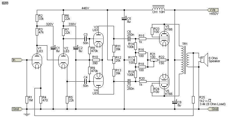
Figure 1.1 - Williamson Valve Power Amp (1947)
The L63 valves were general purpose octal based triodes, common when the Williamson amp was developed. Later versions used either a pair of 6SN7 or 12AU7 twin triodes. Like most valve amps, the circuit is superficially 'simple', but a great deal of the performance depends on the output transformer. This has always been the Achilles heel of valve amps, and an otherwise (close to) perfect design will be laid to ruin by an output transformer that isn't up to the task. The apparent simplicity (assisted by the belief that valves are 'linear') belies the embedded complications. They can all be overcome using the military technique of throwing money at the problem until it goes away, but even finding someone who can wind a good output transformer gets harder all the time.

Figure 1.2 - Mullard 5-10 Valve Power Amp (1952)
Another popular valve design was the Mullard 5-10 (10W) amplifier, using an EF86 preamp, an ECC83 (12AX7) 'phase splitter' and a pair of EL84 output valves. It was never up to the standards of the Williamson, but it was comparatively inexpensive and developed a huge following after its introduction in 1954. Distortion performance was not quite as good as the Williamson (around 0.3% THD at 10W output), but that was considered more than acceptable at the time. While it's a great deal cheaper than the Williamson, it will still require a considerable outlay, particularly for the output and power transformers. To get 10W 'clean' output, the cost cannot be justified.
With the cost of valves today, and considering that you still need a power transformer, at least one filter choke (inductor), two output transformers along with the other parts needed to build two power amps, it adds up to a fairly scary number very quickly. Given the cost/ performance you can get with a modern transistorised amplifier (which beats the Williamson in every respect), I see no point spending perhaps $1,000 for a valve amp that can't equal even a 'lowly' LM3886 power amp IC. Some may choose to disagree, but tests and measurements will quickly reveal which design is superior.
The simple fact is that valve designs have great nostalgia, particularly with people who did not grow up with them. When I went through college, everything was valve based, and I still have some of my old text books as well as many valve data manuals, along with the 'bible' - the Radiotron Designer's Handbook (Langford-Smith). I do admit to the occasional hankering to build a decent valve amp, but my aspirations are tempered by the cost of such an endeavour. It also has to be said that I really don't need another amplifier, and doubly so for one that will cost me a small fortune to build. I have a couple of valve amps (of course I do  ), but they are mono, high-power and not at all suited to hi-if.
Valve life, high temperatures and voltages all work against reliability. Even getting hold of decent valves can be a chore now. They are available of course, but they are expensive, and supply can be patchy. Many of these factors caused great excitement when transistors became available, particularly the ability to build an amplifier that didn't need an output transformer. With no heaters, the equipment could run cooler, and the use of low voltage made everything easier. Alas, everything wasn't as rosy as first imagined, so many early designs were 'sub-optimal' for a variety of reasons.
When transistors were first introduced, it was difficult to get performance that came even close to the better valve amps available. There were some very simple power amps that operated in single-ended Class-A, often using an inductor load. These were no better or worse than single-ended Class-A valve designs that were common in radios (AM, sometimes with SW [short-wave]) and 'radiograms' with an in-built turntable for 78 RPM (and later 331/3 RPM) discs. Most turntables, or more commonly 'record changers' which could hold a stack of discs and drop one at a time, were fitted with a ceramic pickup cartridge.
Many early transistorised amplifiers used techniques that were common in the earliest valve designs, using a drive transformer and an output transformer. In the late 1960s and early 1970s, many transistor guitar and PA amplifiers retained the drive transformer, because it made matching to the output stage much easier. None of these designs was 'hi-if' by any stretch of the imagination. It was only when designers took a different approach that the 'modern' solid state amplifier became viable for home listening.
The designs available now are such that not even the best (and most expensive) valve amps can compete. Output power is higher than (almost) anything built using valves, with lower distortion and wider bandwidth than can be achieved with any of the 'vacuum-state' amps of yesteryear. We are now at the point of diminishing returns - getting 100W with 0.02% THD (and similar levels of intermodulation distortion) is easy and relatively inexpensive.
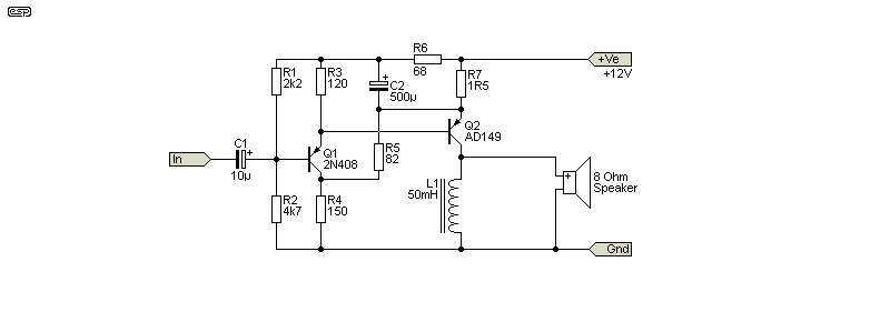
Figure 2.1 - Inductor Load Car Radio Power Amp
The drawing above shows the basics of a 'typical' inductor-loaded power amplifier. The circuit shown is adapted from the original RCA version [ 11 ], and biasing resistors are modified as needed to suit silicon transistors (those used at the time were germanium). As simulated, it can deliver around 3W. The transistors shown were common at the time, with the AD149 rated for a dissipation of 37.5W and able to handle a junction temperature of 100°C (most germanium transistors were limited to 90°C). With a breakdown voltage of 30V, it was used in many power amps until silicon displaced germanium in all but a (very) few niche applications.
The inductor load offers a unique advantage, in that it will (theoretically) allow up to 24V peak-to-peak output voltage with a 12V supply, but this is never realised in practice. The inductor load allowed more power from a 12V car battery than was otherwise possible at the time. With a maximum output power of around 8W, the circuit was a big deal back then. Interestingly, I was completely unable to find an 'official' schematic of one of these amplifiers on the interwebs. Perhaps I was looking in the wrong places, but normally an image search will turn up something other than what I have already published. I ultimately found a circuit in an old RCA transistor manual, and the drawing is adapted from that.
Some car radios used a drive transformer that makes the transistor circuit a lot easier to drive from valve stages. Hybrid car radios were fairly common in the late 1950s and early 1960s. I had one in my car in about 1966. They used valves for the RF stages and the audio preamplifier, with a transistor output stage. Compared to modern units they were very ordinary, but they generally provided marginally more output power than the all-valve car radios that came before.
There's no doubt at all that most designers of the day did their best, but some made serious errors of judgement at times. In their defence, they were dealing with a completely new technology, vastly different from the valve designs that everyone was used to. Low voltages, much higher currents, transistors in an early stage of development and a design process that was at odds with everything they had learned made life hard for a designer. We have benefited from these early designs, because it's human nature to want to do better, and the improvements were rapid. By the mid 1970s designers had produced results that were every bit as good as the best valve designs that came before (often far better), and some of this equipment has since achieved 'cult status' amongst hi-if enthusiasts. Are they really that good? In reality probably not, but that never stopped anything from becoming the 'holy grail'.
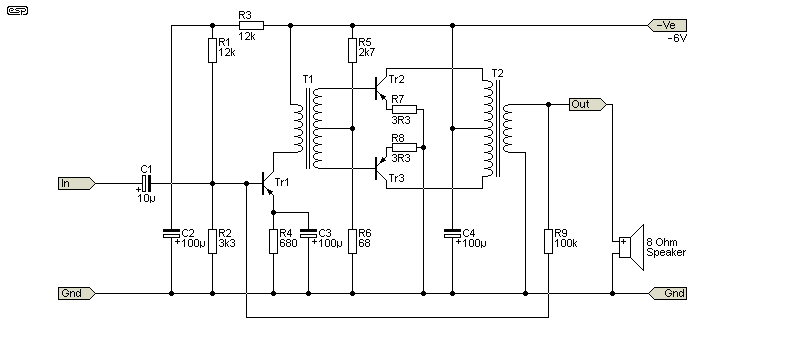
Figure 2.2 - Transformer Coupled With Transformer Output Power Amp
The above is an example of a power amplifier using an inter-stage coupling transformer, along with a transformer output. This design dates from the late 1950s, and is adapted from a book written by Clive Sinclair [ 1 ] (about whom there's more info below). The component values are for a 250mW amplifier, and this was a very common circuit in transistor radios in the 1960s. It's not difficult to scale the parts for more output power, but there's little point. Because the design uses germanium transistors, I can't simulate it. It would be foolish to try to replicate a design such as this, as the requirement for custom transformers would immediately negate the circuit from an economic perspective.
Similar (but actually quite different) high-power (100-200W) circuits were used by many manufacturers (including me) in the early 1970s, using the driver transformer but without an output transformer. The driver transformers were readily available at the time, and were inexpensive. They made it (relatively) easy to build a high-powered amp with the minimum of fuss.

Figure 2.3 - Transformer Coupled With Direct-Coupled Output Power Amp
The circuit shown in Figure 2.3 is an example of a transformer-driven output stage. The trimpots (R7, R11) are used to set both the quiescent current and the DC output voltage. This makes them interdependent, and setup is somewhat fiddly. The output stage itself has a high output impedance, and the feedback is needed to get the impedance down to something passably sensible. The circuit shown can deliver 100W into 4Ω, and the output transistors (Q4 & Q5) were typically operated with zero bias current, with R9 and R13 being low value (around 4.7Ω) and provided output up to 120mA or so. Beyond that, the 'main' output transistors took over. The use of a dual supply is entirely optional, and an output coupling capacitor can be used if the amp is used with a single (positive) supply.
Performance was acceptable for PA (public address) at the time, and they were common in early transistor guitar amps. I still have one of the amps I built using this technique, and it works fine after close to 50 years! Compared to a modern design (such as the P27 guitar amp) it's lacking in most respects, but at the time it was a good amp, and I built them with up to 200W into 4Ω. Needless to say they did not use germanium transistors. The output transistors I used were made by Solitron - 97SE113, and unfortunately no datasheet can be found for them. Several other manufacturers used them as well, and they had a reputation for being almost indestructible. The output stage used driver transistors as well (connected as Darlington pairs) to minimise loading on the driver transformer. The latter used a ratio of 1.5:1+1 which was common at the time. The amps I built used an opamp (µA741) to drive the transformer, but most others used a transistor as shown.
It makes sense to start the (serious) solid-state designs with this amp, because it was introduced as a 'replacement' for the Mullard 5-10 valve design. Stereo was just starting to make serious inroads, so single-channel amplifiers rapidly fell from favour. Valve designs (new or revised) were still being published up until around 1963, but after that they started to fade away. Transistors were expensive, but there was no need for an output transformer. These were often referred to as 'OTL' - output transformerless amplifier. This reduced overall costs dramatically, and the voltages used were far more user-friendly. All the early transistor amplifiers used a single supply, with a capacitor feeding the loudspeaker. The capacitor is unfortunate (electrolytic caps are known to produce some distortion), but it also prevented the speaker from receiving DC if the amplifier failed.
The part designators shown are the same as those in the original 1960 Mullard publication [ 2 ], but I left out the preamp section. That was a very basic transistor design which also used silicon transistors, but has few redeeming features. It included a Baxandall bass and treble control, and while it would perform 'well enough', it's rather poor by modern standards. The circuitry used is discussed at some length in the article Discrete Opamp Alternatives. Note that R14 (100k trimpot) should really be 20k.
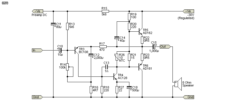
Figure 3 - Mullard 10-10 Transistor Power Amp
An unfortunate consequence of germanium transistors was that being predominantly PNP, the designers chose to use a negative power supply, despite the fact that the AD161/162 devices are complementary (NPN and PNP). This is seen above, with a -30V regulated supply being used. The regulator isn't shown, but was a relatively simple affair, using an AD149 as the series pass device. The AD161/ 162 output transistors use the TO-66 package, and are rated for 30V and 1A, with 4W total dissipation, although the Mullard documentation says they have been 'upgraded'. Released in around 1960, the Mullard 10-10 was a popular design, although it was somewhat underpowered unless the user had very efficient speakers. The published design recommended that the speakers be around 5% efficient - that's equivalent to 99dB/W/m, and very few modern drivers even come close. Even 1% is a big ask, as that means 92dB/W/m.
Another major advantage of these 'new-fangled' transistor amps was that they were much smaller than their valve counterparts. With no output transformers to mount (or pay for!), nearly everything could be installed on a printed circuit board, another 'new' idea back then. A heatsink was needed for the power transistors (also something new), but with such a low power it didn't need to be substantial. Once started, the 'solid-state revolution could not be stopped.
Interestingly, TR3 is a BC108, a silicon NPN transistor. TR3 is the error amplifier, and compares the signal at its base (the input) and emitter (attenuated output). If they are different, TR3 will attempt to make them equal, and any remaining difference shows up as distortion. TR4 (AC128) is the voltage amplifier stage (VAS) which drives the two output transistors. Germanium transistors have a serious temperature dependence, so a thermistor (R26) was used to maintain stable quiescent current. The collector load of TR4 is bootstrapped by C14 to ensure constant current through R20, which improves linearity.
The operating principle of the 10-10 was used by countless other designs, although the idea of a single negative supply rail didn't catch on. As near as I can tell, almost no-one else used it, and the more familiar positive supply took over (at least until amplifier designs started using dual (positive and negative) supplies. Something else that was discontinued very quickly was the use of power transistors without driver transistors, as was used by the 10-10. This made the performance far worse than it could have been, because the error amp (TR3) and voltage amplifier stage (TR4) are loaded more heavily than in later designs. However, it's hard to argue that it used too many transistors. 
R14 (100k trimpot) is used to set the DC voltage at the junction of R22 and R23 to half the supply voltage, with the suggestion to use an oscilloscope to ensure that clipping is symmetrical. The speaker is connected via C15 (1,000µF), which blocks the DC from the speaker. There is no feedback from the output, so capacitor distortion from C15 would be measurable below around 50Hz or so. However, it's probable that any distortion from C15 would be masked by amplifier distortion, quoted as being 0.5% at 1W, rising to 0.8% at 10W output. So, while the 10-10 was certainly cheaper than the valve 5-10, its performance wasn't as good.
The 'El-Cheapo' amplifier (full title: 'El Cheapo 2-30') was published in 1964 [ 3 ], and it has its own page as Project 12A. This was one of the first 'high-power' amps I built, as did many of my work colleagues at the time. Using the then 'state-of-the-art' 2N3055 power transistors, when properly set up it sounded surprisingly good. It was certainly better than low-cost valve amps of the same vintage, and it was surprisingly reliable. Distortion performance was not great, with a simulated THD of 0.14% (the distortion quoted in the article was < 0.6% at 10W output). This is far higher than we expect now, but it was still the equal of most of the affordable valve alternatives.
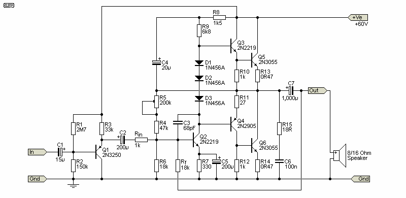
Figure 4 - 'El-Cheapo' Transistor Power Amp
The supply is now the familiar positive voltage, and the power amp 'proper' uses only five transistors. Q1 is an emitter-follower, needed because the amp's input impedance is only 1k. When released, NPN silicon transistors were preferred, because the production processes favoured NPN over PNP (the opposite of germanium). The output stage used is quasi complementary-symmetry, using a compound (Sziklai) pair to 'synthesise' the lower 'PNP' transistor. Q2 is the voltage amplifier stage, and it uses a bootstrapped collector load to increase linearity and output impedance.
The original design included a regulated supply using a germanium series-pass transistor. This was required because the amp circuit has poor power supply rejection (less than 20dB) due to the simple design. and its DC stability is rather poor as well. The output voltage (before C7) is set for 30V with R5 to get symmetrical clipping. All feedback (AC and DC) is returned to the base of Q2, which makes it a 'virtual earth', having very low input impedance. DC feedback is from the output, via R4 and R5. Most AC feedback is provided by Rf, coming from after the output capacitor. This (at least partially) deals with capacitor distortion at low frequencies, but it also creates a low-frequency boost at around 6Hz. Not audible, and generally not a problem.
One potential issue was crossover distortion. This was the bane of most early transistor amps, resulting from a combination of problems. Power transistors at the time had poor gain linearity, so the hFE fell at low and high currents. For low-level signals, the gain reduction at low current reduced the amp's loop gain, so feedback was less effective. Transistor 'bias servo' circuits were uncommon, so there was always a trade-off between bias current stability and low-level distortion. In the original article, it was claimed that there was no crossover distortion, but I know from experience that it did have some, albeit minimal.
While the original title [ 4 ] was probably true when it was written (around 1968 as near as I can tell), it doesn't qualify now. It's a simple design, and is very similar to El-Cheapo in terms of the design. With an input impedance of about 1kΩ it would require an emitter-follower or similar low impedance drive circuit to function properly. It uses the (now very common) bootstrapped collector load (R5, R8 and C3) to improve linearity.

Figure 5 - RCA High Quality 10W Power Amp
There is one technique that's uncommon, even today. D3 and D4 bypass the emitter resistors (R12, R13) when the current exceeds about 650mA. This improves bias stability (quite dramatically) without the losses associated with high value emitter resistors. Of course there's a downside as well, because the diode turn-on/ off is not linear. In the case of a small amplifier, the diodes won't have any effect below ~3W, and that will cover most of the programme material, with only transients exceeding the current needed to cause the diodes to conduct.
This little trick has been around for a long time, but it's not often seen. I used it in the Project 137 powered speaker box amp, but it's uncommon for hi-if applications. By using higher than 'normal' emitter resistors, the bias is unconditionally stable, without any requirement for a bias servo. The THD will be in the order of 0.2% (as simulated), but using modern transistors it may be possible to get it lower. Using high-speed diodes improves distortion performance, but at additional cost (and they weren't available at the time). Still, it's only good for 10W, and an IC amplifier such as the LM1875 (quoted THD is 0.015%) can (allegedly) provide up to 30W. The reality is different, but the point is that simple amps like the RCA circuit are (mostly) irrelevant in the 21st century. However, they can still be fun to play around with.
This particular IC power amp was popular for what seemed like a few days, but was (as near as I can tell) soon abandoned. The Plessey version came in two types, the SL402 (14V supply voltage) and the SL403 (18V). The Sinclair IC was called the IC10, and was presumably a re-badged version of the SL403. Both the Plessey and Sinclair ICs were around £3.50 each in 1969 [ 17 ]. That was quite a bit for an amplifier IC that could deliver no more than around 3 watts!

Figure 5A - Plessey SL40x IC Power Amp Schematic
A notable 'feature' of these ICs was that they used NPN transistors throughout. It was claimed (quite incorrectly) that the large amount of negative feedback would 'eliminate' crossover distortion. Since an amplifier has almost no gain when the output devices are turned off, this is clearly impossible. Simulated distortion was around 0.3% with an 8Ω load at 2W output. A basic distortion analysis indicates that there is evidence of crossover distortion, although it's at a fairly low-level. Unlike many of the other IC power amps, I've not included a schematic for a complete amp (with all external parts in place) as there doesn't seem to be much point.
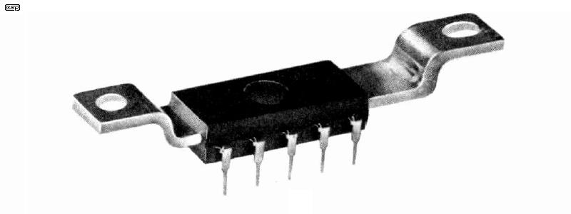
Figure 5B - Plessey SL40x/ Sinclair IC10 IC Power Amp IC
The IC was unusual in a number of respects, particularly the 0.2" (5.08mm) pin spacings and the heatsink bar running through the middle of the package. The IC is shown in Figure 5B, and the IC would be attached to a heatsink, usually of folded aluminium. According to the small amount of info still available, the bar through the middle of the package was steel - an unexpected (and unwelcome) choice due to its poor thermal conductivity. Expecting the IC pins to support the weight of the heatsink (especially in transit or if the amp were dropped) was 'adventurous' to put it mildly, and the all NPN transistor design is unique. I have seen all NPN circuits used before to obtain a push-pull output stage, but never for a power amplifier. It's a credit to the designers that they got it to work as well as it did, but it could never be classified as 'hi-if'. The integrated 'preamp' (a 'triple' Darlington) is an interesting addition, and that allowed a complete amplifier with active (Baxandall) tone controls to be built with a single IC - two for stereo.
The Armstrong 600 [ 5 ] was very advanced for its time (ca 1970), having very low distortion (simulated at ~ 0.02%, published THD 0.08%). The output transistors are RCA 40636 devices, which had very similar specifications to the 2N3055 (90V, 15A, 115W), and the output stage is quasi complementary-symmetry. Bias (quiescent current) is set by two diodes (D2, D3) and a trimpot (R11). There is no adjustment for the output DC voltage, and when simulated it was necessary to change R2 from the original value of 82k to 100k to obtain symmetrical clipping. With an 82V supply, the output devices were pushed very hard, especially if the amp was used with 4Ω speakers. However, that was presumably never a problem when these amps were in service.
Figure 6 - Armstrong 600 Transistor Power Amp
The designers have gone to a great deal of trouble to get everything right. Q1 is the error amplifier (all component designators are mine - the original schematic showed illegible reference details). To ensure that the gain of Q1 isn't compromised by loading, it buffered by an emitter-follower (Q2) before the voltage amplifier stage (Q3). The collector load of the VAS is bootstrapped as with the previous designs shown, and the output stage is again quasi complementary-symmetry. R11 is used to set the output stage for a quiescent current of 20mA.
The frequency compensation capacitors appear to be sub-optimal (at least in a simulation), but were no doubt correct for the original devices used. This design was probably at the pinnacle of what was achievable at the time, but it's not at the end of the design process. Overall this amp would withstand scrutiny today, but only if the test procedure were blind. A sighted test would cause people to think they could hear the output capacitor (it's enclosed in the feedback path so it effectively ceases to exist for the audio frequency range).
The Sansui AU-101 was built between 1973 and 1975, and is rated for 15W/ channel into 8Ω The circuit diagram is adapted from the service manual, including the component designators. It uses a single 44V DC supply, and although not shown, the power supply filter cap was only 1,000µF. The design is fairly simple, but (apparently) it sounded very good, based on a couple of reviews I came across. It includes feedback from after the output capacitor (C817), and the input transistor (TR801) gets DC feedback via R811 and R813, with all AC feedback via the output cap, R815 and C807.

Figure 7.1 - Sansui AU-101 Transistor Power Amp
The service manual is very detailed and has complete circuits for the preamps and power amps. As with most Japanese designs, the transistor types are uncommon, and in this case they appear to have been selected for particular parameters (especially gain). A simulation is inconclusive because the exact transistor types are not available as simulator models, but substituting common devices available today it seems to perform well. The specifications were written in the 'bad old days' when 'music power' was commonly quoted. In this case they claim 44W 'music power' into 8 ohms, a figure that is quite impossible into any typical load.
Although rated for 15W/ channel, the amp can provide 20W for short periods, until the main filter cap discharges under load. Distortion is claimed to be less than 0.8% THD at rated power, with response from 20Hz to 60kHz (±2dB). Overall, it should be capable of decent performance, but it's not as good as the Armstrong described above. Under normal listening conditions I'm sure that it would produce an 'acceptable' listening experience. In some areas, the AU-101 is considered a 'classic', but in reality it's just a reasonably competent amplifier, with a very basic preamp (not included here).
Another 'classic' of the late 1970s was the NAD 3020. At a claimed 20W/ channel it was no powerhouse, but it was something of a bargain when it was released in 1978. The amp itself is fairly basic, but the number of phase compensation capacitors throughout the circuit is somewhat baffling. As a current feedback amplifier it should need only a couple of caps at the most (the Sansui uses just one). The output is directly connected to the speaker via a small inductor (no output capacitor).
Apparently (I can't verify this with any certainty), NAD sold over 1 million 3020 integrated amplifiers, and there are many websites where the authors sing the praises of this amp. When released it was cheap, but people quickly discovered that it also sounded very good. I don't do reviews of any kind, but there are some very dedicated followers, and I didn't see anything to indicate that it's not beloved by all. While it's rated for 20W/ channel, the ± 30V supplies will let the amp deliver 40W into 8Ω.
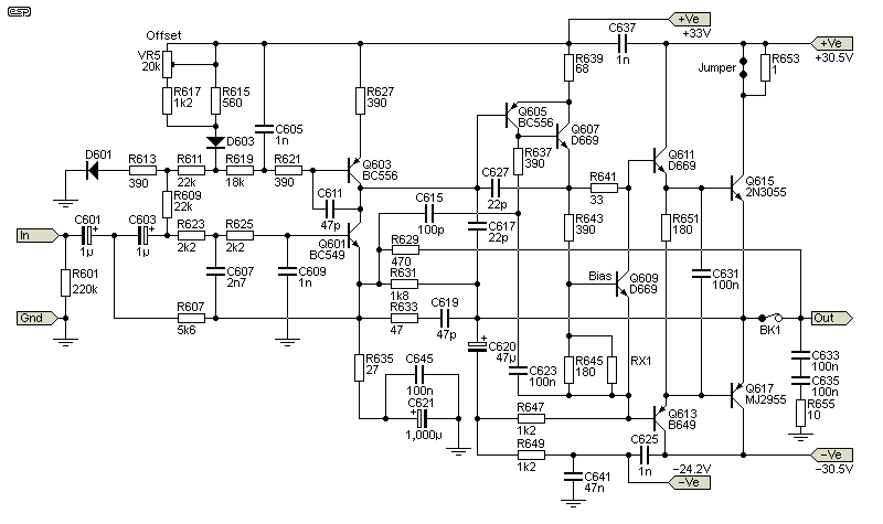
Figure 7.2 - NAD 3020 Transistor Power Amp
To minimise any distortion that might be created by 'BK1' (a part that isn't mentioned in the parts list - it appears to be a circuit breaker), the majority of the feedback is applied via R629 (470Ω). BK1 is normally closed, but if it opens, enough feedback is available through R631 (1.8k) to prevent amplifier malfunction. Continuing with assumption that 'BK1' is a circuit breaker, failure to apply feedback from the speaker side would decrease damping factor (and it may be non-linear).
There are a few other things that are different from most other amps. Firstly, there are no emitter resistors for the output transistors. That makes the bias setting critical, and it's been designed so it's not user-adjustable. Factory setup would add a resistor in 'RX1' position to obtain the desired quiescent current. R653 is a 1Ω resistor, and is normally shorted. The jumper is opened to allow quiescent current to be set to the recommended 30mA by measuring the voltage across the resistor.
The second oddity is the combined 12dB/ octave high-pass and low-pass filters at the input (C601 to C609 and associated resistors. The low-pass filter provides ~1dB of boost at 20Hz, with a -3dB frequency of 12Hz. The low-pass filter is 3dB down at about 50kHz. Thirdly, the amp is powered from an unregulated dual supply, and the two 'odd voltage' supplies are regulated and are used for the preamp section. Next, the DC offset circuitry is the most elaborate I've come across, using a transistor (Q603), several resistors and a trimpot, plus two diodes.
Finally, the power amp has an in-built (switchable, but it cannot be disabled) 'soft clip' circuit (not shown) which may or may not provide any benefit. Very few other amps have used it, as all it really does is increase distortion as the maximum power is approached. NAD seems to be the only manufacturer who's used it in more than one design.
Sinclair was always something of an outsider when considering high-quality amplification. Clive (the late Sir Clive - 30 July 1940 - 16 September 2021) was ever the entrepreneur, and was responsible for the first Class-D (pulse-width modulation - PWM) amplifier, the X10. To say it was an unmitigated disaster is probably high praise, and it vanished from the market after what seemed like a few minutes. Like many Sinclair products, it used whatever transistors that could be acquired for the lowest cost possible. It was claimed (but I have no details) that Sinclair often purchased transistors that were 'factory rejects', being devices that failed to meet specifications.
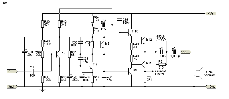
Figure 8.1 - Sinclair 10W Transistor Power Amp
I have very little information on the first amp shown, only a schematic of the complete unit - preamp, power amp and a power supply that incorporated active current limiting. The latter was diode-fed from the emitter resistor of TR11, and was designed to turn off the power supply if the peak current exceeded ~18A or so. It's rather doubtful that it would provide much protection, as that much current could easily damage the output transistors. As you can see, no transistor part numbers are shown. That's because they weren't shown on the only circuit diagram I have, and it's likely that they changed depending on what was available (at low cost) at the time.
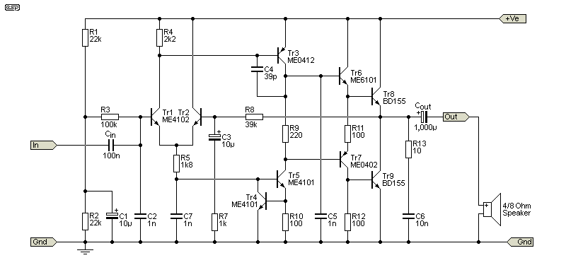
Figure 8.2 - Sinclair Z50 Transistor Power Amp
The Z30/ Z50 Sinclair amps [ 6 ] were early adopters of the now common long-tailed pair for the input stage. In addition, the bootstrapped load for the voltage amplifier stage has been changed to a current source. A current source provides a small advantage compared to bootstrapping, but it also limits the output swing because it cannot boost the collector resistor for the VAS above the supply rail. I've always liked the simplicity of the bootstrap technique, and the difference between an 'ideal' current source and a bootstrapped version is small. Predictably, the Z30 amp uses the same circuit as the Z50, but with some component changes.
The quasi complementary-symmetry output stage (still used with the Z30 and Z50) was one of the last things to disappear, when PNP power transistors finally became available with specifications that were close to those for NPN devices. They are still not identical, but are much closer than an NPN Darlington stage used with a complementary (Sziklai) pair. Interestingly (or not), there was considerable effort spent on making a Darlington and Sziklai pair perform equally. This was never a complete success though.
Before true IC power amps (of reasonable power) came along, Sanyo and a few other manufacturers made hybrid modules. These included the semiconductors, resistors and some low-value capacitors encapsulated within the hermetically sealed case. While the technique was used as early as the 1950s, audio power amps came along much later. They featured a metal back, screen printed 'wiring' and generally used transistors in die form (without additional packaging). More information is available on the specific techniques used from Wikipedia [ 7 ]. The circuitry used is actually fairly basic, with a quasi-complementary output stage. The higher power versions required external emitter resistors for the output stage, as they used two power transistors in parallel.

Figure 9 - Sanyo STK4042 Thick Film Hybrid Power Amp
The STK4042 [ 8 ] (80W into 8Ω, with ±45V supplies) is shown as an example, but there were many more, covering a wide range of output powers. While they appeared to make life easier for hobbyists and commercial manufacturers, the reality was always different. The number of external parts needed was generally quite large (see Figure 9B for the wiring diagram), and it was very difficult to build an amplifier using them without a PCB. Specifications varied, with output powers ranging from 20 to 200W, but with rather uninspiring distortion figures for the most part. Later versions were better than their predecessors, but they are no longer made (at least not by Sanyo as near as I can tell). These modules can still be found on eBay, but that's a risk I wouldn't take.
Like almost everyone involved in audio, I used them for a couple of 'quick & dirty' jobs, and while they certainly worked well enough, it didn't take much of an accident to cause them to fail. The basic idea was not too bad, the additional external parts count made them a lot less convenient than they appeared at first. Stereo versions were even less attractive, because there were more pins that had to be connected to external parts, with very close spacing. I suspect that the only reason anyone sells them now is for servicing equipment with failed modules, although a few die-hard hobbyists may still think they're a good idea.
The main disadvantage is that if (when) a module fails, the entire unit has to be replaced. There may only be one internal device (or connection) that's faulty, but the modules are not able to be serviced due to the way thick-film hybrids are made.
For quite a while now, power amps have been available as integrated circuits. One of the earliest was the LM12, and this is the only one with a circuit diagram shown here. There are several IC power amps that have been used in ESP projects, the LM386, LM1875 (or TDA2050), LM3876, LM3886 and TDA7294. Of these, the LM3876/ 3886 and TDA7294 are genuinely able to be called 'hi-if', with the LM1875 not too far behind. The LM12 had a somewhat unusual 4-pin TO3 case. Unlike almost all modern 'power opamps', it's compensated for unity gain and can be used as a high-power buffer. The absolute maximum supply voltage is ±40V, but ±30V is recommended. I1 to I4 are current sources.
I was able to simulate the circuit pretty much as shown, and it works quite well. Distortion (as simulated) is a little disappointing at 0.06%. Clipping recovery is not very good, and it shows evidence of 'rail-sticking', where the output remains 'stuck' to the supply rail for a few microseconds after the voltage should have recovered. Q14 and Q15 are transistors connected as diodes, and are required because of the protection circuitry which isn't shown in the datasheet. Q7 is an oddity that only appears in ICs, having two emitters. This can be simulated by using two transistors with their bases and collectors joined, but that won't work with discrete transistors unless they're well matched.
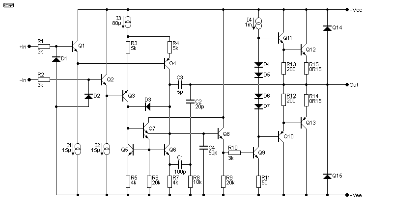
Figure 10 - National Semiconductor LM12 Power Amp (Protection Circuits Not Included)
The LM12 is no longer available. The circuitry is fairly straightforward, and it has the 'traditional' long-tailed pair as the input stage, buffered with a pair of emitter followers. The LTP (Q3 and Q4) has considerable degeneration caused by the two 5k resistors (R3 and R4). The LTP is loaded by a current mirror (Q5, Q6 & Q7), and Q9 is the VAS (voltage amplification stage). The LM12 was capable of very low distortion (the datasheet claims 0.01%). With ±30V supplies it can deliver about 80W into 4Ω. It was a useful IC, but more modern replacements can provide more power with lower distortion. The modified TO-3 package would be very expensive if made today (as are all TO-3 transistors).
The modern hi-if IC amplifiers are probably 'state of the art', and they are mostly very competent. It's highly unlikely that anyone would pick one in a true double-blind test, regardless of the competition. They offer high performance in a compact package, needing relatively few external parts. I tend to think of them as 'power opamps', because they are generally used very much like any 'normal' opamp. One thing to be aware of is the circuit gain. Most are designed for a closed-loop gain (set by feedback) of at least 20dB (×26 voltage gain). If you attempt to use them with less than that oscillation is probable.
There's a couple of other things that you need to be aware of as well. Because the surface area is fairly small, the rated power is certainly available, but expecting any of them to provide full sinewave power for an extended period will usually cause them to overheat and shut down. Provided the source is music, this rarely (if ever) causes a problem. The protection circuitry of the National Semiconductor (now Texas Instruments) parts is vicious, and it has a hair-trigger. My suggestion is to operate them at the lowest voltage you can, consistent with acceptable power output. Many commercial amplifiers use IC power amps, particularly for 'budget' products.
Some manufacturers have focussed on the convenience of these parts, and they are used in many low-cost guitar amplifiers. This is not recommended, because they are prone to failure if pushed hard for extended periods. Several guitar amps using them are well known for failures, and I would never recommend any IC power amp for that role. For serious listening, I have no hesitation using or recommending them - it's probably the easiest way to build a power amplifier (or five).
By way of comparison to the previous examples, Figure 10 shows A simplified version of the Yamaha AX-490 power amplifier. There is one added transistor (in the VAS - voltage amplifier stage), and simply introducing one extra transistor makes stability worse, and requires more (and more complex) phase correction networks. The circuit as shown simulates quite well, and it appears to be stable, but without the exact transistors specified that's not assured.
Figure 11 - Yamaha AX-490 Power Amp
This is not intended as an example of the 'best' amplifier available by any means, but it is representative of many designs found in commercial equipment from Japan. While it's likely that a true audiophile will scoff, the overall design is solid, and the AX-490 has respectable specifications. The reason for showing this circuit was to demonstrate the extra lengths that designers have to go to, to ensure stability when the basic design is 'improved', even if ever-so-slightly. As designs become more complex, ensuring unconditional stability just gets harder.
As anyone who has looked at schematics for Japanese audio equipment will be aware, they often come up with 'quirky' solutions and their design ideas are somewhat different from designs from 'the west'. Mostly, they are no better or worse, but the designers tend to look at things differently. This is a good thing, because often you can discover a better way to do things, but of course not all ideas are necessarily 'good'. For example, using one pair of 200W output transistors with ±55V supplies is really pushing the limits of the transistors' safe operating area (SOA). With a 4Ω resistive load, the peak dissipation is over 140W for each output device, and there's absolutely no room for error (or operation at elevated temperature)!
As a final design, Figure 11 shows the principles that are used in most modern designs. Not everything is used, depending on the designer and the expectations for the circuit. The current source (Q6) may be replaced by a bootstrap circuit, the current mirror (Q4, Q5) may be replaced by one or two resistors, and the VAS (Q7, voltage amplifier stage) may be a Darlington or compound pair. The output stage may use Darlington or Sziklai pairs, and the output inductor (L1) and its parallel resistor may not be used.
No component values are shown, because this is an example, and is purely intended as a demonstration of the basics of an amplifier where most of the designer's 'tricks' are shown. Even so, there remain untold variations. The input stage may use PNP transistors (with others for the current sources and mirror reversed as needed), the phase compensation (aka 'dominant pole') capacitor (C4) may be repositioned, and additional compensation may be needed elsewhere.
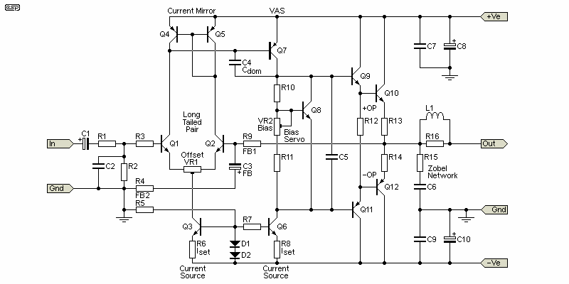
Figure 12 - Generalised Schematic Of A Modern Power Amp
Along with the above, the offset preset (VR1) may be omitted, and in some cases even the bias preset may be replaced with fixed-value resistors. Some designers will duplicate the input stage to obtain an aesthetically symmetrical input stage, which may or may not provide an actual improvement. The idea of a 'fully symmetrical' amplifier is actually a myth, because the NPN and PNP transistors will always be different. Considering how hard it is to get identical transistors of the same polarity, it's unwise to assume that PNP devices can ever be identical to their NPN counterparts. Matched pairs can be obtained, but they will almost always be NPN or PNP, not both.
As a generalised scheme, it's not possible to show every possibility, and even output stages can be far more complex than the simple arrangement shown. Paralleled output transistors are often used to boost output current capability and/ or ensure that the devices operate within their safe operating area, or simply to allow the use of cheaper (lower power) output transistors. Other variations include using JFETs for the input stage (always with reduced gain), and they may be arranged in cascode with BJTs to recover the gain lost by the JFETs. Sometimes a second LTP is employed to get the highest gain possible, but compensation becomes much harder.
The general scheme shown is comparatively simple, but it incorporates many of the design ideas that give good performance. Simplification does not necessarily mean that a design is sub-optimal, and using all of the schemes shown likewise does not mean that the design is 'better' than another. All design involves compromise, and some things will do nothing other than make the final design more complex, with no guarantee that performance matches the degree of complexity.
Stabilisation against oscillation becomes harder as a design is made more complex, and a particular design will often demand that the exact same transistors are used as specified. Since different devices have different ft (frequency transition), using other than the specified devices can lead to instability, with the requirement to modify the compensation circuits to prevent oscillation. Any amplifier will oscillate if the open-loop gain is greater than unity at a frequency where the phase shift equals 180°. This causes negative feedback to become positive.
Of course, there are countless variations on the basic theme shown. Some work very well even though they appear to be much simpler, while others perform worse, even though more complex. A great deal depends on the output transistors, and modern devices are far better than their early counterparts. In particular, it's important that the output devices have sufficient gain at low current - especially around the bias (quiescent) current. Early transistors exhibited considerable 'gain droop' at low current, so at low output levels they didn't have enough gain to allow negative feedback to work effectively. If the circuit has low gain, it must also have reduced feedback (in direct proportion), so distortion increases.
Class-D amplifiers are gaining in popularity, with some of the latest offerings being every bit as good as a Class-B amplifier. They are not without their own special issues of course, but they have the advantage of running much cooler than any purely linear amplifier. Because the output devices are either 'on' or 'off', the problem of high power dissipation during normal operation is relieved. The dissipation of the output MOSFETs (invariably switching types) is low, but there can still be high dissipation as one MOSFET turns on as the other turns off. In the following drawing [ 13 ], the pin marked 'DT' is used to control the dead time - a period where both MOSFETs have zero drive voltage. Extending dead-time is safer for the MOSFETs, but increases distortion.
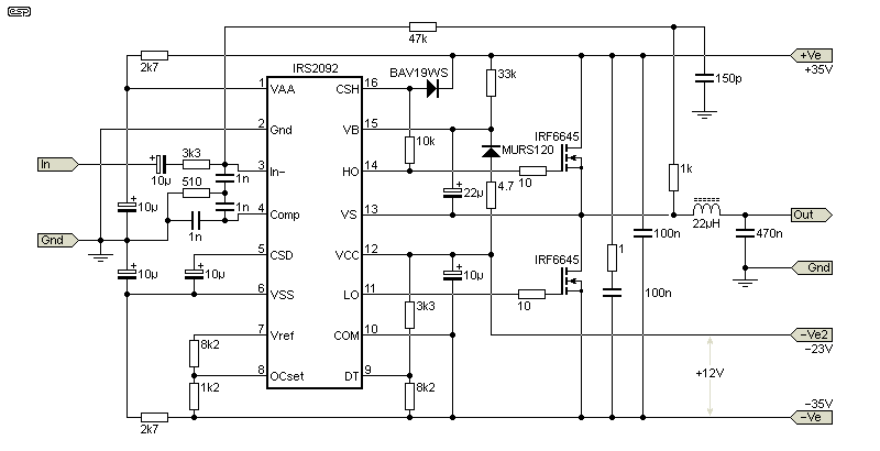
Figure 13.1 - IRS2092 Based Class-D Power Amp
The schematic shown is one of a series of designs published by IR (International Rectifier), using the IRS2092 Class-D IC. This is a self-contained Class-D circuit, which incorporates the PWM (pulse width modulation) circuitry, along with MOSFET gate drivers (high-side and low-side), as well as over and under voltage protection. While it's no longer 'state-of-the-art', it is a capable IC, and untold thousands of Class-D amplifiers have been built using it, with many still readily available as kits or modules. Capable of operation at ±100V (although that's the upper limit), it can (at least in theory) be used for amplifiers of up to 2kW output. This requires a number of changes, with dedicated gate drivers and more (and bigger) MOSFETs.
The circuit shown is claimed in the datasheet to provide 120W into 4Ω, with distortion below 0.1% for any output below 100W. The design is a self-oscillating type, using a Sigma-Delta converter internally to convert the analogue audio into PWM. The nominal quiescent oscillation frequency is 400kHz, but this can be changed if required. The circuit shown is a little misleading in a few respects, in that it only shows the basic circuit. To obtain full protection (particularly for over-current of DC fault conditions) requires external circuitry, as does the separate 12V supply (indicated as -23V).
This is intended as an example only, and I used it because it's a very common 'discrete' Class-D amplifier, although it's now a fairly old design. Many Class-D amps available now are a self-contained IC, requiring only a few external parts. One of the biggest issues (and the reason I've not done a Class-D amp project) is the output inductor. This is critical to filter out the high frequency (400kHz) noise, and it, along with the 470nF capacitor shown, determine whether the amplifier creates unacceptable radio-frequency interference or not. Radiated RF can be notoriously difficult to remove, and the performance of the output filter is critical. The inductor also requires very low series resistance to prevent signal loss and/ or poor damping factor.
Up until fairly recently, a semi-discrete solution such as the one shown above was the only option, but that's changed with fully integrated designs now seeming to dominate the Class-D sector. There are many modules available, both from online auction websites and other vendors. Some are very good, while others manage to screw up the design to produce a 'product' that's worse than useless. However, of the better options, you'll come across quite a few using TI (Texas Instruments) ICs, most of which are pretty good (as long as the PCB is well designed). These are invariably SMD, with a great many pins, and are not suitable for most hobbyists to assemble at home. NXP (Philips) also has a range of ICs, with the following being a good example ...
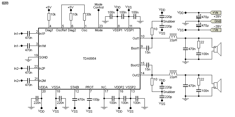
Figure 13.2 - Fully Integrated Class-D Power Amp (TDA8954 - Shown as Stereo SE)
The above is an example of one of the current Class-D ICs available [ 14 ]. The TDA8954 also has a number of relatives, with different output power ratings. This is a single IC 2-channel SE (single-ended) or mono BTL amp, capable of up to 420W into 8Ω. Distortion figures are comparable to many Class-AB amplifiers, and they are rated for a maximum supply voltage of ±41V. They aren't as flexible as the TI version described briefly below, with a minimum load impedance of 8Ω when used in BTL (There is no option to parallel the two channels). Unfortunately, this does limit their usefulness somewhat, especially if you need to drive a subwoofer, as most are 4Ω. The drawing is simplified, but shows most of the important 'stuff'.
Note the speaker connections and input wiring. This is designed to operate one channel with the opposite phase to prevent 'bus-pumping'. a phenomenon common to Class-D amplifiers. Depending on the load impedance and input frequency, one or the other supply voltage may transfer energy to the other, causing it to rise - possibly to a level that will cause the amp to shut down. Operating the two channels with opposite phase is the most effective way to prevent this.
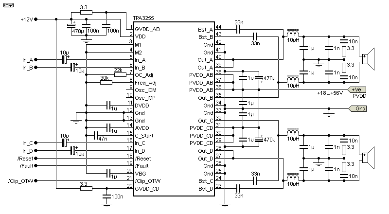
Figure 13.3 - Fully Integrated Class-D Power Amp (TPA3255 - Shown As Stereo BTL)
The TPA3255 [ 15 ] IC has four independent amplifiers, and it can be operated as 4 × single-ended (capacitor output) amps, 2 × BTL (bridge-tied-load) amps, or a single parallel BTL (PBTL) amp, capable of driving a 2Ω load. Quoted distortion is 0.01%, but that varies with the load impedance. The maximum total output power is about 600W, either as a single mono PBTL amp, two stereo BTL amps, or four single-ended amps. Other than a substantial number of capacitors, it's pretty much self-contained, with only a few resistors for setting various parameters. It requires more external parts than the TDA8954, and it has 44 closely spaced pins with a thermal pad on the top of the IC. I don't propose to go into any more detail, as everything you need to know is in the datasheet.
Needless to say, there is a wide variety of different Class-D ICs available, with most from the established manufacturers. Some are very good indeed, while others are probably best classified as 'alright'. When used for internal TV speakers and other applications where poor quality sound seems to be acceptable, product manufacturers will likely use whatever they can get cheaply. Despite any misgivings one might have, few of the ICs are actually 'bad' per se. They are often let down by the PCB layout or extreme cost-cutting. There is no doubt that some of the modules available fall into the latter category (I have a couple that had to be modified because of a major error in the PCB layout).
One thing to be aware of with most Class-D implementations is the output filter. It's designed to remove the oscillator frequency and allow the audio through, but it also can make the amplifier load impedance dependent. The high-frequency response changes, depending on the load. Ideally, all Class-D amps would include a Zobel network to set a predictable impedance at frequencies above 15kHz. Even more ideally, this would be included in the speaker box, so that it will present a known (and non-variable) impedance at around 20kHz. I don't recommend that anyone should hold their breath while waiting for this.
Note that this article is simply a collection of ideas. The operating principles for transistor power amps are consistent through all the designs. An input stage operates as an error amplifier, followed by the voltage amplifier stage. The VAS drives the output devices, which can use several different topologies. Some of the engineering concepts are now considered outdated, but all remain as valid today as they ever were. Not every concept shown here has been validated by simulation, and the drawings are taken from datasheets, service manuals or from my collection.
I must point out that the circuits shown are not intended for construction, although you can do so if you wish (do not expect any support as it won't be forthcoming). They are provided as examples of the progression of amplifier designs over the years, and as such are a very small selection of the countless designs that have been produced. Many of the transistor designs shown here use an output coupling capacitor, something that was discontinued by most manufacturers by the 1980s or thereabouts.
However, while the majority of new designs don't use an output cap, it is still used in some configurations. This is typical with some IC (integrated circuit) designs where the constructor has the option of using a single-supply (positive only) IC as two or four amps in a single IC. The idea is that amps can be used in BTL (bridge-tied-load) with two amps used in anti-phase for higher power (the speaker is connected between the outputs), or the amps are used independently. With a BTL connection, there's no need for a coupling capacitor to the speaker, because the two outputs are at the same voltage (anything from 6V to 40V DC). If the amps are used independently, an output coupling capacitor is required to block the DC. Many Class-D ICs use this technique, as does the low-power LM386 amplifier IC.
For reasons that I find puzzling (to put it mildly), many new designs are fully DC coupled, so response extends from DC up to the maximum claimed frequency. We can't hear DC and loudspeakers can't reproduce it either, and there is absolutely no reason to faithfully amplify any DC that may exist at the input. It doesn't take much DC to cause speaker damage, so this trend is most unwelcome, IMO. There's a sub-set of audio 'enthusiasts' who imagine that capacitors are 'evil' and damage the sound in mysterious ways. While it has been demonstrated by many experts in the field of electronics that many capacitors create some (usually small) amount of distortion, it has to be noted that even the worst capacitor in the world can't introduce distortion if there's no AC voltage across it. By making coupling caps larger than necessary for a given LF -3dB frequency, distortion becomes a non-issue!
A capacitor used to handle speaker current is in a different league. The 'ripple current' through the capacitor is the RMS current delivered to the speaker. For high power amps, this becomes a serious limitation, so elimination of that cap has much to commend it. Using an input capacitor remains very important, as without it, a DC fault in a preamp (or DAC) can easily destroy one's loudspeakers. As noted, if the cap is sufficiently large, there will be almost no AC voltage across it, so distortion is not a problem other than at very low frequencies ... where the speaker will introduce far more distortion than any capacitor.
Many modern designs are (IMO) somewhat over-designed. I do accept that aiming for the lowest possible distortion (for example) is a worthy goal, but there comes a point where further improvements are not worth the added complexity. Particularly if you build your own audio 'stuff', an amplifier so complex that it takes forever to get it to work isn't a good idea (and in some cases a constructor may never complete a complex project). ESP project amps (with or without PCBs) are mostly designed specifically so they are easy to construct, yet give performance that's in line with expectations. There are many designs that may offer higher performance, but beyond a 'respectable' set of specifications they become hard to put together, and usually require the exact transistors specified or performance is dramatically affected.
As design complexity increases, so do issues with stability. An amplifier that cannot be made stable (i.e. no high-frequency oscillation, whether continuous or parasitic, and the absence of ringing on transients) isn't usable. Unless the hobbyist has a good oscilloscope, even knowing that there is oscillation can be challenging, because most people don't recognise the symptoms. If you make your own PCBs, few amateurs are aware of the subtle distortions that a poor layout can introduce. A bad layout can couple 'dirty' signals on the supply rails into the audio path, and it's not at all difficult to double the distortion without even realising it.
The most recent development is Class-D [1, 2], using PWM (pulse-width modulation). Some are very good indeed, and others fall into the same category as mentioned in the introduction. They are 'adequate', but in some cases don't come close to even the low standards set in the early 1970s, However, they are capable of much higher power than anything available back then. There are now many IC versions (readily available from various on-line sites), usually available as fully built modules. These can work well but may not, for a variety of reasons. Having tested some of these, I know first-hand just how bad some of them really are [3]. Buyer Beware!
¹ Class-D does not indicate or imply that the amplifier is digital. While some Class-D amplifiers do have digital processing, the conversion from analogue to PWM is usually a purely analogue process (although this could be argued when Delta-Sigma [ΔΣ, aka ΣΔ] modulation is used). The term 'Class-D' was coined simply because we already had Class-A, Class-B and Class-C, so Class-D was next in the sequence.
² Tripath coined the term 'Class-T' (® registered trade mark) for its PWM ICs, but technically it's still Class-D. While many claims were made that Class-T was 'superior' to conventional Class-D, there's little evidence to back that up. Indeed, that's been a historical issue with audio, as there are far more opinions than facts presented on innumerable websites.
³ As an example, I have two different boards using the ST TDA7498 IC [ 16 ]. One is essentially unusable, having high (and very audible) distortion and poor performance overall (even after correcting a major PCB layout error). The other is fine to listen to, with no audible artifacts even at the onset of clipping. The good one sounds almost identical to by workbench LM3886 amplifier, although a proper blind A/B test is difficult in my workshop environment which has 'dubious' acoustics. (Sighted tests are always invalid!)
Apart from a number of circuits that I've collected over the years (many of which cannot be reliably identified), the following publications were used to compile this article. There are many other designs that could have been included, but many are so similar that it would only be repetition. Those shown are fairly representative of the progress of power amplifier design over the years. It's likely that I have omitted someone's favourite circuit, but this is an article, not a book.
While there were more sites (and datasheets) that I looked at during the course of writing this article, most were either to verify that I had not made errors in the drawings, or to double-check some of the facts presented. A few of the circuits were simulated (none of the valve or Class-D designs though), and the simulations matched the descriptions fairly well (within the normal error range for a simulation vs. a constructed amplifier).
| Main Index Articles Index |