
|
|
| Elliott Sound Products | Project 12A |
Based on information supplied by a reader, I have learned that my recollection of the El Cheapo design was rather badly flawed. It seems I had mixed up recollections, and merged a couple of completely different designs into one - none of which resemble the original El Cheapo in any way.
Originally designed by R.R. Moore and published in Audio Magazine (November 1964 edition), the design is presented more for historical interest than as a recommended design. While not a bad amp by the standards of the day, it will be found lacking if compared to any more modern offerings. This will apply even using the latest transistors, because the amp has very limited open loop gain. To some people, this is seen as a benefit rather than a limitation, but it does mean that low-level non-linear distortion will be higher than you are used to.
The amp was called "El Cheapo 2-30", and was rated at a maximum of 30W per channel into 16 Ohms (which used to be a very common speaker impedance). It used a single regulated power supply and capacitor coupled speaker. Having a scan of the original, I can now reproduce the exact circuit details. It was a very simple amp, and used quasi-complementary symmetry for the output stage. For those younger than I who have no idea what I'm talking about, quasi-complementary symmetry was a scheme used in the days when PNP power transistors were expensive and silicon devices were pretty much useless. If you wanted any sort of voltage and current rating, you had to use NPN devices. The quasi-complementary output stage used a (discrete) Darlington for the positive side, and a complementary pair for the negative (i.e. a PNP driver coupled to an NPN power transistor).
Meanwhile, in those days, if you wanted high gain and reasonable current capacity, germanium transistors still ruled supreme. Provided they were used in applications where leakage was not a major problem, germanium devices worked very well - this did not really include the output stages of power amps though. Back then the majority of loudspeakers were 16 Ohms, with only a few venturing down to 8 Ohms. Anything lower than that was almost unheard of in 1964.
Figure 1 shows the circuit - it was a cheap amp compared to most offerings of the day. It also managed to sound respectable - again by comparison - and I built a couple as did many of my friends of the day. For hi-fi, PA systems and even guitar amps (but they weren't much good at that), El-Cheapo was everywhere at the time!
Note that the transistor types are the original specified devices. Most are obsolete now, but a list is shown below of suitable candidates.
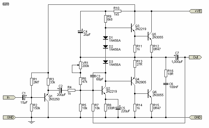
Figure 1 - Original El-Cheapo Circuit
These were the days when the 2N3055 was the pre-eminent power transistor (NPN of course), and there were no vaguely equivalent PNP devices for less than about 5 times the price, and even these were highly inferior. As a result, the quasi-complementary output was very common, and indeed this is still the case with most IC power amps. The quasi-complementary output stage was the most popular until relatively recently, until decent PNP power devices became more readily available. Immediately, just about everyone started using NPN and PNP Darlington coupled devices for the output stages (as shown for Q3 and Q4) - the funny part is that it was demonstrated back in the mid 1970's that the full Darlington connection actually sounds (or at least measures) worse than quasi-complementary stages. Is not progress a wonderful thing?
The input stage of the El-Cheapo is not subject to the phase problems of the long tailed pair, since the Class-A driver (or VAS - Voltage Amplification Stage) is used as the input. Amps driven in this manner tend to be inherently stable. There is a major problem with DC offset of course - the input is referenced to the negative supply. If this is earth (ground) then it's not an issue, but it precludes using this design with a dual supply. The DC was not a problem with capacitor coupled speakers.
As shown, the gain for audio frequencies is 18 (25dB), which means an input sensitivity of 1V for an output of 40W. The closed loop gain is set by R4 and R7. Since the feedback is taken after the output coupling cap, the latter has no influence on the low frequency response - however, this arrangement creates an under-damped filter network that causes a 4.5dB peak at about 5Hz. Increasing C7 to 4,700µF eliminates this problem for all intents and purposes.
In the original article, there were several variations of the design, however I will only present the amp in basic 40W form here. The variants were mainly based on using lower supply voltages, but included a dual (parallel) output stage for the odd low impedance load. Note that D1-D3 should be mounted so their bodies are in contact with the heatsink, but as I recall this wasn't mentioned in the original article.
Note that the amp is inverting, and the input impedance of the power amp itself is 1k (R4). Because of this, there is an emitter follower (Q1) before the amp proper to convert the impedance to something usable. The arrangement shown is less than ideal though - a better solution would be to delete everything to the left of C2, and drive the circuit from an opamp (C2 would have to be reversed if the opamp uses dual supplies).
| Transistor | Original | Replacement |
| Q1 | 2N3250 | BC559 |
| Q2 | 2N2219 | BD139 |
| Q3 | 2N2219 | BD139 |
| Q4 | 2N2905 | BD140 |
| Q5 | 2N3055 | TIP35C |
| Q6 | 2N3055 | TIP35C |
As expected, the overall performance of the amp is somewhat less than stellar. Output power into 8 ohms is about 40W, and distortion was simulated at 0.14% - far higher than we expect these days (the original article claimed 0.6% which is even less acceptable). A major part of the problem is that the amp uses a single gain stage - Q2. This limits the open loop gain and therefore the amount of available feedback, so output stage non-linearity cannot be effectively improved to the degree we expect from more modern designs. However, considering the age and simplicity of the design, it gave a reasonable account of itself for its day.
The power supply was specified as regulated, and for a single supply amp with low open-loop gain this is a good idea to maintain low hum levels. Using a regulated supply is not normally desirable, but in this case was probably warranted. Germanium transistors were used as shown in Figure 2 (all medium and high power germanium transistors are/were PNP). Since the amp will have a PSRR (Power Supply Rejection Ratio) of only about 36dB, supply noise will be a problem with an unregulated supply. It is worth noting that the emitter follower stage (Q1) contributes most of the supply noise - another good case for driving the amp from an opamp stage.
The regulator is only simple, but would have worked well enough as shown - at least at low current. High current performance can be expected to be woeful, because there's no feedback and inadequate filtering. The Zener diode would normally be a 62V 1W unit, to obtain a 60V supply voltage for the amp (equivalent to using ±30V with a more conventional split supply). By the standards of today, the filter caps are much too small (as is the speaker coupling cap), but I am presenting this as it was originally described.
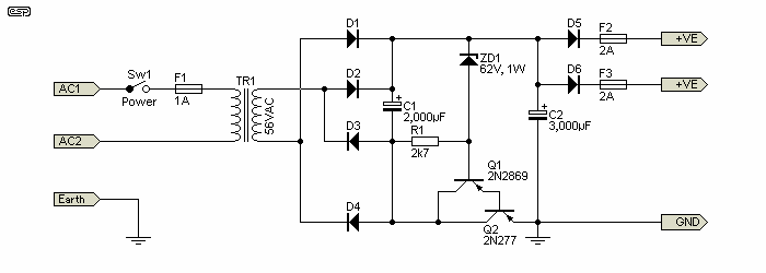
Figure 2 - The Original Power Supply (Using Germanium Transistors)
I have spared readers the potential agony of various different supply voltage options, as well as the pilot lamp and its ballast resistor (LEDs? In 1964? The LED was only invented in 1962, and was still a curiosity when this design was published). If anyone really wants to build an original El-Cheapo then I'm sure you can work the details out for yourself. In case you may consider asking ... No, I will not assist. Same applies for the germanium transistors originally used - they are totally obsolete, and there is simply no point even attempting to get them. The capacitor values are no longer available, and are too small anyway.
All diodes should be rated at 5A minimum, and 400V types should be used. The benefit and usefulness of D5 and D6 is rather suspect. No reason was given as to why they were included, but modern practice would be to leave them out altogether. I suggest that they are omitted, as shown in Figure 3. Today it would also be normal practice to use a reasonable sized electrolytic capacitor (1,000µF or so) directly across each amplifier's supply (after the fuse, and close to the power amp itself).
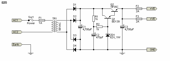
Figure 3 - Power Supply Modified to Use Silicon Transistors
The regulator shown in Figure 3 is a better proposition these days, and silicon NPN transistors can be used for Q1 and Q2. A single Darlington device could also be used. It may be necessary to reduce R1 and R2 from the 1k Ohms shown, depending on the gain of the transistors. Again, I will leave that to prospective constructors (assuming that anyone wants to build one). 
Despite initial appearances, the two regulator circuits are functionally (almost) identical. Since the circuit of Figure 3 is likely to be the most commonly used (if it is ever used), and suitable transistors would be BD139 for Q1, and 2N3055 (or TIP35C) for Q2. The extra resistor and capacitor improve regulator performance dramatically, and ripple is reduced from 1.6V peak-to-peak without C2, down to less than 40mV p/p when it's included, both at an output current of 3A. It also limits the initial input current to C3 so that the peak dissipation of Q2 is not exceeded. There was no provision for this in the original circuit (Figure 2), and peak dissipation in Q2 could reach several hundred watts as the second filter cap charged.
The transformer secondary should be 56V RMS, and this will give an unregulated voltage of around 77V with no load. That means that only 17V will be dropped across the regulator, and with a worst case current of well under 4A (both channels, and assuming 8 Ohm speakers!) the peak dissipation will be around 38W - the average will be a lot less. Transformer rating is around 250VA - a lot higher than you'd expect because of the regulator.
Needless to say, the regulator requires a heatsink as well as the amplifier output transistors, so you will spend a lot more on heatsinks than components. The mains fuse will need to be a slow-blow type, and the amp supply fuses must be fast blow.
There's not a great deal to say about the amp. It is simple, and as such may appeal to some readers. The three diode string sets the bias, and it will be found to be quite variable in real life. Ideally, the diodes should be mounted in contact with the heatsink, but if the sink is adequately sized this may not be necessary. I recommend that it be done regardless.
The input capacitor is much larger than it needs to be, and there is a real benefit if it is reduced to 1µF. Since input impedance is about 50k at the base of the emitter follower (Q1), a 1µF input cap will still provide a -3dB frequency of just under 4Hz - provided the output cap is increased to 4,700µF.
With an open loop gain of only 180 (45dB), there is not as much feedback as we are used to with modern amps. However, the amp remains essentially flat to 10kHz open loop, and this is dramatically better than most amps having a massively high open-loop gain. Because of the small amount of feedback, it may be thought that output impedance would be somewhat higher than we have come to expect. This is not the case though, and Zout will normally be less than 100 milliohms (a damping factor of >80 for an 8Ω load).
Speaking of feedback - because the input stage creates an inherently stable amp, there is no reason to expect that TIM (Transient Intermodulation Distortion - assuming that you believe it exists of course ¹) will be a problem, since feedback is simply applied to the base of the input amp, and very little frequency 'compensation' is needed. Although a 68pF cap was specified for the original, it should be possible to reduce this if wider open loop bandwidth is your goal.
Construction is non-critical, within the normal bounds of amplifier building at least, and will not be discussed in any detail. I will, however, make the following observations ...
 Main Index
Projects Index
Main Index
Projects Index