
|
| Elliott Sound Products | Amplifier Basics - How Amps Work (Part 5) |
 Main Index Main Index
 Articles Index Articles Index
|
There are some circuits in the world of electronics that are just too useful. While some have been around for many years, others only became practical with the advent of the transistor. The circuits described are a mixture, some are very old, and others much newer.
I shall not go into the history (this is an electronics tutorial, not a history lesson), but will show the various stages in their basic form for each type of circuit.
On the topic of current sources, sinks and mirrors, click here to see the full article describing how they are most commonly used in audio circuits (and why).
The constant current source (or sink) is one of the most versatile and widely used of the circuits shown in this section. The ideal current source provides a current into a load that is independent of the resistance (or impedance) of the load, from zero to infinity. As always, the ideal does not exist, but within the capabilities of the power supply voltage, it is quite simple to do, and surprisingly accurate.
There is no real difference between the two circuits - one sources current (or sinks electrons) or vice versa. Sometimes it might help to consider the circuit 'upside down' to see that there is no real difference, only one of terminology.
As an example, if we wanted to supply a current that were fixed at 1A into any load impedance, then we might use a circuit similar to that in Figure 5.1 - a basic transistor current source. As shown, this will supply 1A into any resistance from zero Ohms up to a little under 50 Ohms. The power supply is the limiting factor - to be able to supply the same current into 1M Ohm would need a 1,000,000V power supply, which is an unrealistic expectation.
The current source or sink can be imagined as a device with infinite impedance - this must be the case if the current remains unchanged even as the load resistance is varied over a wide range. Naturally, the impedance of actual current sources is not infinite, but can easily reach values of many megohms, even in a simple circuit.

The operation of the circuit is simple. If the voltage across the emitter resistor of Q2 attempts to exceed 0.65V (the base turn-on voltage for a silicon transistor), then Q1 will turn on, and short out all base current to Q2 except for exactly that amount required to maintain the specified current of 10mA (10mA through 65 ohms develops 0.65V). If the collector current of Q2 falls, then the voltage across the emitter resistor also falls. This turns off Q1 until the current is again stable at the preset value. (This is only one way to make a current source - there are many others.)
Thermal stability is not good. The emitter-base potential falls at 2mV / degree C, so as the temperature increases, the current will fall from the nominal 1A. At low temperatures, the opposite will occur. A precision voltage reference can be used, or an opamp can monitor the voltage across the resistor, resulting in a much more stable current. Fortunately, in most circuits, it is not that critical, so the circuit of Figure 5.1 is very common.

Junction FETs, being a depletion mode device, can be used as a current source very easily, as shown in Figure 5.2. Because JFETs are mainly low current devices, the useful range is from about 0.1mA up to 10mA or so. This is ideal for many of the circuits that need a current source. The actual current is dependent on the FET's characteristics, but is sufficiently stable for many non-critical applications. Based on the FET curve shown in Figure 3.2a, this current source will supply a current of about 0.4mA into a load from zero to 72k Ohms. The voltage is also lower, because of the lower voltage rating of most FETs.
The current mirror is one of the 'new' circuits, and works well with bipolar transistors. It is unusual to see this circuit implemented with valves or FETs, and I will not change this (i.e. I will show transistors only). Figure 5.3 shows a simple current mirror (this version is not very accurate, but is still extremely effective and commonly used).

Any current injected into the collector/base circuit of Q1 (via Ri) will be 'mirrored' by Q2, which will draw the same current through its load resistor (within the capability of the transistor and power supply). Current mirrors are sometimes used as current sources (one less resistor), and are not as dependent on temperature, since both transistors will ideally be at the same temperature. It is not uncommon to use dual transistors (or thermal bonding) to ensure stability.
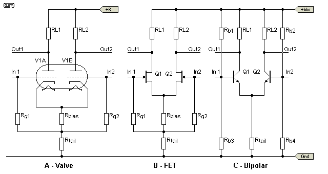
The long tailed (or differential) pair is an old circuit, and is used with valves, FETs and BJTs. It was originally designed in the valve era, and provides a means for the comparison of two voltages. The long tailed pair (LTP) is used as the input stage of most opamps, and many (if not most) modern power amplifiers.

As can be seen in Figure 5.4, the LTP can be made using valves (A), JFETs (B) or bipolar transistors (C). Valves and JFETs can be self biased as shown, but BJT circuits must have external bias resistors. A pair of MOSFETs could be used, but at the typical currents used (less than 5mA), the gain and linearity would be very poor. Although each circuit is shown using a resistor as the 'tail', in FET and bipolar circuits this is most commonly a current source (or sink if you prefer).
The use of a current source stabilises the overall current, so the device input current is not affected by supply voltage changes, or variations in the input bias voltages.
In each case, the circuit has an inverting and a non-inverting input, and an inverted and non-inverted output. Application of the same voltage and polarity to both inputs at once results in (theoretically) zero output - this is called the common mode signal, and is commonly quoted for opamps as the common mode rejection ratio.
The valve and FET versions only require capacitive coupling, as they are self biasing as shown. The bipolar circuit cannot be self biased, and requires the biasing resistors Rb1 and Rb2 for each input.
The output of each version may be taken from either or both outputs, and may be capacitively or direct coupled. Direct coupling is very common with LTP circuits, especially in opamps and audio power amplifiers, where it is the rule, rather than the exception.
When used as the input stage of an amplifier, the LTP uses one input as the signal input, and the other is used for the application of feedback, in the same way as in an opamp.
It's worth noting that the performance of a long tailed pair is dependent on the gain of the active device. BJTs have far greater gain than valves or JFETs, and the performance of a BJT version is generally vastly superior to the valve or FET circuits. Of the three circuits shown, only the BJT will be able to provide close to identical outputs (but with one inverted of course). The other two certainly work, but the level difference between the outputs can be 20% or more.
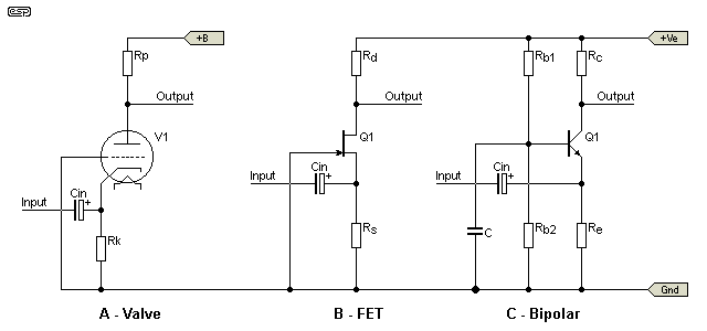
Sometimes, it is desirable to have an extremely low input impedance, for example where the output impedance of the source is very low. One way to achieve this is to use the control element (grid, gate or base) as the reference, and apply the signal to the cathode, source or emitter (as appropriate). Figure 5.5 shows an example of grounded (or common) grid (A), gate (B) and emitter (C).

Apart from having an extremely low input impedance, this class of amplifier has an additional advantage. The normal capacitance from output to input is bypassed to earth, and no longer acts as a feedback path. Such circuits are therefore capable of a much better high frequency response than when used in the 'conventional' way, and are common in radio frequency circuits. The bypass path is direct for a valve or FET, and is via a capacitance for the bipolar circuit.
All inputs and outputs must be capacitively coupled, unless the preceding circuit is to be direct coupled (unusual) or the output is direct coupled to a follower (quite common).
Because the input impedance is so low, there are few applications in audio, except where this circuit is used in conjunction with a 'normal' amplifier stage. This forms a new circuit, called cascode.
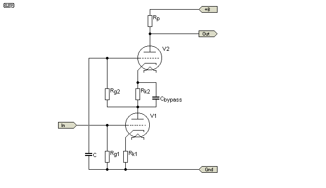
This circuit was developed in the valve era, primarily to obtain better response at high radio frequencies. Valves have capacitance between the plate and grid, and this acts as a feedback path at high frequencies, causing a drop in gain as the frequency is increased. This is the so-called 'Miller' effect. Operating in cascode allows the circuit to have a high input impedance (via the normal grid input), and the grounded grid amplifier (the signal is applied to the cathode) means that there is no feedback from plate to grid, and the grid acts as a shield to prevent feedback to the cathode. The lower half of the stage contributes a relatively small amount of gain, and is not subject to the feedback effect since it is operating as a current amplifier (there is very little voltage swing on the plate, so there is little or no signal to feed back).

As can be seen, the grid of V2 is earthed via the capacitor for all signal frequencies, allowing V2 to operate as common grid. The capacitor (C bypass) is used to ensure that there is no gain lost due to cathode degeneration (local feedback). The cathode of V1 will also be bypassed in many cases, especially where low noise is a primary goal.
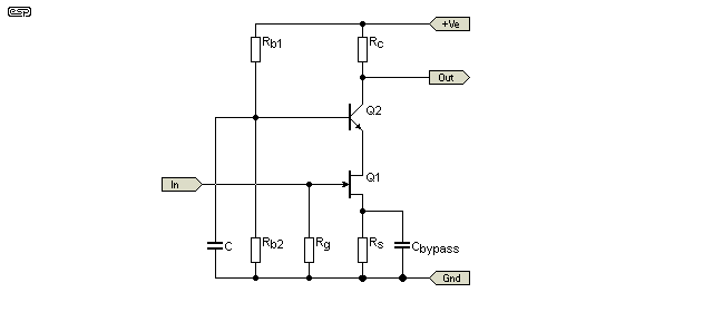
The same principles can be applied to FETs or BJTs, and has similar advantages. The capacitance between Drain and gate (or collector and base) is isolated in the same way as with a valve circuit, with the signal being coupled to the source or emitter by the first device. Figure 5.7 shows a composite JFET / BJT cascode circuit, which will have better linearity than a conventional amplifier, and a much better high frequency response.

This type of circuit is not uncommon in high performance opamps, where very wide bandwidth and good linearity before feedback are required. Cascode circuits are also sometimes seen in solid state power amplifier circuits, where the designer is trying to obtain the maximum possible bandwidth from the amp.
The base of Q2 is grounded to all signal frequencies, so the stage operates as a common base circuit. Using a JFET as the input element means that the circuit has a high input impedance, while the BJT ensures maximum gain. To obtain even more gain, Rc might be replaced by a current source, in which case the gain from this single stage can exceed 1000 times, with wide bandwidth and excellent linearity.
Previous (Part 4 - Opamps) Next (Conclusions)
 Main Index Main Index
 Articles Index Articles Index
|