

|
| Elliott Sound Products | Amplifier Basics - How Amps Work (Part 3) |
 Main Index Main Index
 Articles Index Articles Index
|
Now on to FETs and MOSFETs. FET stands for "Field Effect Transistor", and MOSFET means "Metal Oxide Semiconductor Field Effect Transistor". This topic is something of a can of worms, not because of some deficiency in the devices, but because of the huge array of different types. The basic FET types are ...
There are a couple of major sub-classes of MOSFET - lateral and vertical. Lateral MOSFETs are particularly suited to audio applications, as they are far more linear than their vertical brethren, although their gain is lower. Vertical MOSFETs (e.g. HEXFETs and their ilk) are ideally suited to switching applications, and this includes Pulse Width Modulated (PWM) amplifiers.
Note: Further to the material here, I suggest you also read the article Designing With JFETs. It's much more recent than this article, and describes the use of JFETs in some additional detail. It also provides some info that will come in handy when you discover that your favourite JFET is no longer made, something that's depressingly common and it's getting worse.
The terms 'lateral' and 'vertical' refer to internal fabrication methods, so many others you may come across (such as HEXFETs ®) are essentially variations of the vertical process. This is still not all the possibilities, because there are additional sub-classes as well, particularly with switching MOSFETs. However, for the purpose of a general article on their characteristics and how they work, I will concentrate on the most commonly used versions. This narrows the field, and we are left with both polarities of junction FETs, and both polarities of enhancement mode MOSFETs. With these, we cover the major proportion of current designs, so even 'though I will be leaving out a lot, the stuff I leave out is not all that common (he says hopefully).
FETs are 'unipolar' devices, in that they use only one polarity of carrier, in contrast to bipolar transistors, which use both majority and minority charge carriers (electrons or 'holes', depending on the polarity). FETs are far more resistant to the effects of temperature, X-Rays and cosmic radiation - any of these can cause the production of minority carriers in bipolar transistors).
I shall concentrate only on three terminal FETs, and the terminals are ...
There is no simple equivalent circuit for FETs (as there is for transistors), but this is of no consequence. The gate is the controlling element, and affects the electron flow not by amplifying a current (as in the transistor), but by the application of a voltage. The input impedance of junction FETs is very high at all usable frequencies, but MOSFETs are different. They have an almost infinite input resistance, but appreciable capacitance between the gate and the rest of the device. This can make MOSFETs hard to drive, because the capacitive loading makes most amplifier devices unhappy.
The junction FET is common in the inputs of high performance opamps, and offers extremely high input impedance. Indeed this is the case for discrete FETs as well, and a simple voltage amplifier using a junction FET and a power MOSFET are both shown in Figure 3.1. Both devices are N-Channel, and note that the arrow points in a different direction for each. The arrows point in the opposite direction for a P-Channel device, and all polarities are reversed. Vdd is +20V.
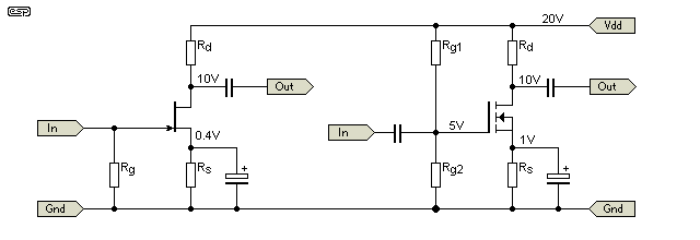
Junction FETs are depletion mode devices, and (like all depletion mode FETs and MOSFETs) can be biased in exactly the same way as a valve. Depletion mode means that without a negative bias signal on the controlling element (the gate), there will be current flow between the drain (equivalent to plate or collector) and source (equivalent to cathode or emitter).
An enhancement mode device remains turned off until a threshold voltage is reached, after which the device conducts, passing more current as the voltage increases. Although there are MOSFETs made for low power operation, the majority (in audio, anyway) are power devices. These are almost exclusively enhancement mode, and can be capable of very high current.
In Figure 3.1, the power MOSFET is an enhancement mode device, and the junction FET is depletion mode. These are the most commonly used in audio. Enhancement mode power MOSFETs are also used in switching power supplies, and are far better than bipolar transistors in this role. They are faster, so switching losses are not as great (therefore the MOSFETs run cooler), and they are more rugged, and able to withstand abuses that would kill a bipolar transistor almost instantly.
This ruggedness (coupled with the freedom from second breakdown effects), means that MOSFETs are very popular as output devices for high power professional amplifiers. In this area, the MOSFET is second to none, and they are firmly entrenched as the device of choice for high power.
This is not to say that this is the only place MOSFETs are used. There are many fine audiophile power amps (and even preamps) that use power MOSFETs, and there are many claims that they are sonically superior to bipolar transistors (again, a debate that I will not discuss here).
Somewhat like valves, FETs and MOSFETs are very device dependent, and it is not normally possible to just substitute one device for a different type. Also like valves, the gain that can be expected from a voltage amplifier circuit is device dependent, and the manufacturer's data sheet (or testing) is the only way that one can be sure of obtaining the gain required in a given circuit.
The characteristics of FETs must be covered in two parts, since we are dealing with two quite different devices. The first will be the junction FET, and as with transistors, I shall only describe the N-Channel, but virtually identical P-Channel devices are available (although not as commonly used).
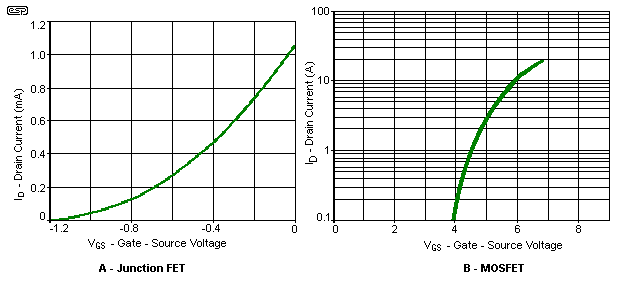
Initially, so the transfer characteristics of the two devices can be seen side by side for comparison, Figure 3.2 shows a fairly typical device from each 'family'. The junction FET data is from a 2N5457, and the MOSFET is an IRFP240 (a vertical MOSFET - more suited to switching applications).
Rather than show the input and output signals superimposed on a graph, this time I show only the graph itself. These are excerpts from manufacturers data, but with a small catch - Figure 3.2b has the drain current displayed on a logarithmic scale, so the linearity of the device cannot be seen properly. If this graph were redrawn as linear, it will show that linearity is best at higher currents (on the graph shown it looks the other way around), and the device becomes almost perfectly linear with drain currents above about 3A.
Note that because the junction FET is depletion mode, drain current is highest at 0V gate-source voltage. The (most common) MOSFET on the other hand is enhancement mode, so at 0V gate-source, there is no current. Conduction starts at 4V, and by 6V the drain current is 10A (for example). This varies by MOSFET type, and they are available with low threshold (suitable for driving from 5V logic) or 'normal' threshold, requiring up to 10V or so for full conduction.
| The term Siemens (S) is now replacing Mhos as the unit of transconductance in most literature: 1S = Mho (1µS=1 µMho). For the above graphs, it may be worked out that the junction FET has a transconductance of 1,500µS, and for the MOSFET it is approx. 9,000µS (9,000 µMhos) |
Like valves, FET data sheets provide gain information as gm (mutual conductance - in µMhos). The junction FET shown has a gm of (typically) 1,500 µMhos (in the graph shown it is actually closer to 1425 µMhos in the linear section), which translates to about 1.5 mA/V.
The most common of the quoted parameters for junction FETs are
The process of amplification is almost identical to that of a valve, except that the voltages are lower. The device is biased in the same way (although fixed bias can also be used). This means that the gate must be reverse biased with respect to the source, with the gate having the opposite polarity of the source-drain voltage.
FETs offer low noise, especially with high impedance inputs, and in this respect are the opposite of bipolar transistors, which are generally at their best with low source impedance.
Junction FETs are predominantly low power, although there are some high power devices available. These are uncommon in audio applications.
It's notable (and regrettable) that many manufacturers have 'rationalised' their range of JFETs. Many of the high performance devices we used to be able to use in (for example) very low noise circuits have disappeared, and you can almost see JFETs vanishing from supplier catalogues as you watch. While I have never believed that JFETs have some 'magical' property that makes them sound better than anything else, it would have been nice if the manufacturers hadn't just decided that we don't need these specialised devices any more. I only have a couple of designs that use FETs, and it's now difficult to find devices that are suitable.
Again, MOSFET data sheets also provide information similar to junction FETs, but there are more items of importance to the designer. The most useful of these are
Enhancement mode MOSFETs pass virtually no current when there is no gate voltage present. To conduct, a voltage must be applied between source and gate (of the same polarity as the drain voltage). Once the threshold has been reached, the device will start to conduct between drain and source.
At increasing gate voltages, the drain current increases until either a) the maximum permissible drain current or total dissipation limit is reached, or b) the drain voltage falls to its lowest possible value. In this instance, since the source-drain channel is now fully conducting, the value of RDS(on) determines the voltage.
Typical power MOSFETs offer extremely low on resistance, with values of less than 0.2 Ohm being fairly typical. There are many devices with much lower values (<50mΩ), but this is only important in switching circuits. In an audio amp, the MOSFETs should never be turned completely on, since this means the amplifier is clipping.
Another area that must be addressed with MOSFETs is the voltage between gate and source. Because the gate is insulated from the channel by a (very) thin layer of metal oxide, it is susceptible to damage by static discharge or other excessive voltage. It is common to include a zener diode between source and gate to ensure that the maximum voltage cannot be exceeded. Voltage spikes in excess of the breakdown voltage of the insulating layer will cause instantaneous failure of the device.
Again, I have shown both a junction FET and a MOSFET in Figure 3.3, both common-drain or source-follower circuits. As can be seen, the junction FET is biased almost identically to a valve, but all voltages are much lower. The MOSFET requires a positive voltage, and this must be greater than the source voltage, by an amount that takes the characteristics of the MOSFET into consideration. For the device characteristics shown in Figure 3.2 this means that at a current of 100mA, the gate must be 4V higher than the source.
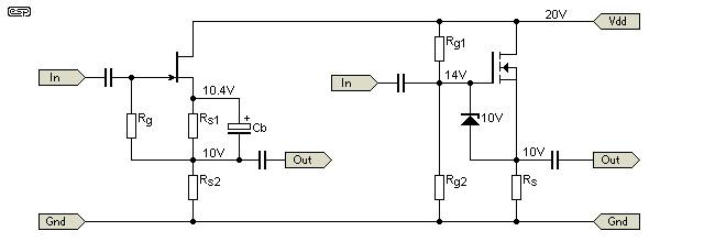
For the JFET source follower, the bypass capacitor (Cb) is not always used, in which case the output would normally be taken from the source. When Cb is included, the output level is the same at both ends of Rs1, and input impedance is much greater because Rg is bootstrapped. The input impedance increase depends on the transconductance of the FET. For the JFET circuit shown(with Rg being 1MΩ), input impedance is about 5MΩ if Rs1 is not bypassed, rising to around 18MΩ with Cb included.
Cb needs to be large enough to ensure that the AC voltage across it remain small at the lowest frequency of interest. For example, if Rs1 is 1k, Cb must be at least 10µF (a -3dB frequency of 16Hz). A higher value is recommended to minimise low frequency distortion. For normal audio work, I'd use at least 33µF (still assuming 1k for Rs1).
Included in the MOSFET version is a zener for protection of the gate insulation. A 10V zener is used, as this gives good protection and is still able to let the maximum possible MOSFET current flow. A 6V zener could have been used, and this would still allow current up to 10A, which is far more than can be achieved from this simple circuit.
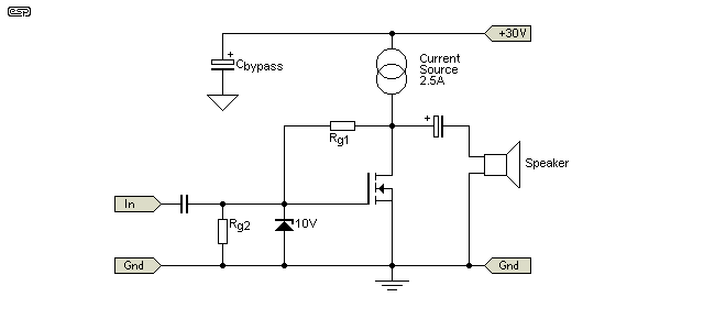
In exactly the same way as a power valve can be used in single-ended Class-A, so too can a MOSFET. A simple circuit is shown in Figure 3.4 which will provide about 10W of audio. Using a constant current source as a load (as shown) gives better efficiency than a resistor, and improves linearity. The distortion from a circuit such as that shown will be roughly the same as that from a single ended triode valve circuit. Overall efficiency will be higher, since there is no cathode bias resistor needed, and no heaters as with a valve. Performance is not up to hi-fi expectations !
Although there are a few, all MOSFET power amplifiers are uncommon. Most use a combination of bipolar transistors (for the input and gain stages), and MOSFETs for the output devices. This seems to be the most popular circuit arrangement, so I will concentrate on this. Figure 3.5 shows a fairly typical arrangement (in simplified form), and the operation of this is almost identical to that of an amplifier using bipolar transistors in the output. Note that emitter followers are needed to be able to provide the low impedance drive that MOSFETs need, although in some circuits they are not used. Instead, the Class-A driver stage (Q3) is operated at a higher than normal current to allow it to drive the MOSFETs properly.
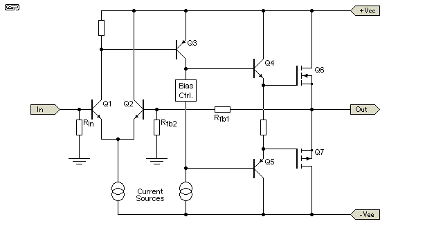
One problem with this arrangement is that the gate to source voltage represents a circuit loss, so the power supply voltage needs to be typically ±6V higher than the required peak output voltage to the load to turn on the MOSFETs fully. Although this is not a major problem, it does increase dissipation in the output stage, and the loss increases with lower impedance loads.
Some (especially very high power) amps get around this by using a low current (but higher voltage) secondary power supply for the drive circuit, and the main high current supply for the MOSFETs. In an amp using +/-50V at 20 Amp main supplies, the secondary supply might be ±60V, but capable of perhaps 1A maximum.
As with the bipolar amp (did you notice how similar they are?), I have not included components for stability. These are typically the same as for a standard bipolar transistor amp, but will usually include 'stopper' resistors in series with the gates of the MOSFETs, and sometimes additional capacitance to prevent parasitic oscillation - the need for these varies from one device type to the next.
The surface is again, only barely scratched. The junction FET (aka JFET) is ideally suited to circuits where high impedances are expected, and will give the lowest noise. They are an invaluable electronic building block when used where they excel - providing extremely high input impedance.
Like all devices so far, JFETs have their limitations ...
There is generally an ideal (or close to ideal) amplifying device for every application, and when used properly, the JFET is extremely versatile and at its best when high impedances are needed. If you have a need to send an amplifier into space, then JFETs are preferred due to their greater 'radiation hardness'. However, parameter spread is high, so no two JFETs can ever be assumed to be the same, even from the same batch. Where operation is critical, JFETs must be matched or provided with an adjustable source resistance to allow the operating point to be established.
JFETs (in fact all FETs) are more sensible than bipolar transistors when heated, and problems of thermal runaway are not usually encountered with these devices.
Most of the 'better' JFETs for audio use have now disappeared from the market. The 2SK170 was revered in some quarters, and was the 'go to' device for very low noise in many different applications. The original and any replacements that were offered subsequently are now obsolete. You might be able to buy JFETs with '2SK170' printed on them, but what's inside is anyone's guess. One thing you can be fairly sure of - it almost certainly will not be a genuine 2SK170. The LSK170 made by Linear Systems is available, as is as good as the original.
Even many 'pedestrian' JFETs have all but vanished from supplier's inventory, leaving you with limited choices. Some are available if you can handle SOT (small outline transistor, SMD), but even there the range is nothing like it used to be. This situation continues to get worse with each passing year.
The MOSFET is one of the most powerful of all the current range of amplifying device, with extraordinary current handling capability. Ideally suited to very high power amplifiers, switchmode power supplies and Class-D amplifiers, where extremes of operating conditions are regularly encountered, the MOSFET has no equal. The possible exception is the Insulated Gate Bipolar Transistor (IGBT) which is a hybrid device as the name implies. IGBTs are not covered in these articles.
... And, as always, there are limitations ...
To some extent, all the above can be forgiven when you really need the capabilities of a MOSFET. The freedom from second breakdown and the massive current capabilities of MOSFETs are unmatched by any other active device. With a properly designed drive circuit, MOSFETs are also very fast, capable of performance that is generally superior to that of bipolar transistors. This is not very helpful in audio, but is essential for switching circuits. Note that the 'freedom from second breakdown' is (or was) often cited by manufacturers, but there is a failure mechanism that's almost identical, and is invoked when a switching MOSFET is used in linear mode. Most manufacturers state that their MOSFETs are not intended for linear operation. If you decide to do so, then be prepared for unexplained failures.
Coupled with a positive temperature coefficient that can stop thermal runaway in a linear circuit (when proper precautions are taken), the (lateral) MOSFET is almost indestructible, provided that you ensure the gate voltage is kept below the breakdown voltage. It's also essential to keep the drain voltage below the maximum specified.
The positive temperature coefficient can be a help in audio circuits, although it can be a problem in switching power supplies, since the 'on' resistance also increases with temperature, and in a switch-mode power supply this can cause thermal runaway (exactly the reverse of bipolar transistors in this application).
Switching MOSFETs are by far the most common now, with many of the earlier 'lateral' MOSFETs now unavailable. Project 101 was designed to use lateral MOSFETs, and it simply won't work with switching MOSFETs (not only because the gate and source pins are reversed for the two types. Switching MOSFETs are not designed for linear operation, and have to be severely derated to prevent failure.
Previous (Part 2 - Bipolar Transistors) Next (Part 4 - Opamps)
 Main Index Main Index
 Articles Index Articles Index
|