
|
|
| Elliott Sound Products | Designing With JFETs |
 Main Index
Articles Index
Main Index
Articles Index
JFETs (junction field-effect transistors) are beloved by many, but unfortunately the range has shrunk dramatically in the past few years. This has made it very difficult to build some of the more esoteric designs from readily available types, but Linear Systems produces a range that's ideal for many designs. I mention this because they kindly sent me some samples (full disclosure here) of two different types. One of these is the LSK170B (equivalent to the revered 2SK170, but with graded maximum drain current). Having received these, I decided that it was a worthwhile exercise to look at the basic design processes for JFET stages in general.
JFETs provided by Linear Systems notwithstanding, most of the designs shown use a rather pedestrian 2N5484. I used this because it's one of the few low-cost JFETs that you can still get from (some) major suppliers, and it has basic specifications that make it ideal for general-purpose low current applications. It doesn't excel at anything in particular (although it does have fairly low noise of around 4nV√Hz), but it also has few 'bad habits'. This is important when experimenting, as it makes it more likely that you'll have a successful outcome.
I have avoided the more complex designs, simply because they are complex, and because you need to go to considerable trouble to match the JFETs closely enough to get a working circuit. While JFETs have many desirable features, they also come with many challenges. One of the advantages is that because the gate is a reverse-biased diode, there is far less likelihood that any stray radio-frequency signals will be detected and amplified, as can happen easily with BJTs (bipolar junction transistors) and many opamps (operational amplifiers). The challenges are covered below, and they are not insignificant.
As noted within this article, I have very few designs that use JFETs. This is not because I dislike them (quite the opposite), but because the range from most of the larger suppliers has been reduced to a few devices intended for switching, rather than linear operation. They do work as amplifiers, but some have so much input capacitance that they are unusable with high-impedance signal sources. The few remaining devices from the major suppliers are often only available in a surface-mount device (SMD) package, making it next to impossible to use traditional prototyping systems such as a breadboard or Veroboard. While you can use a small adapter board (available from a few suppliers), this is still a nuisance, as each device you wish to test or experiment with needs its own adapter.
The really low noise devices such as the 2SK170 are gone ... other than on eBay, where you might get a JFET of one type or another, but it's unlikely to be genuine. Linear Systems makes the LSK170, which is pretty much a direct equivalent, but they aren't available from most major distributors. 'General Purpose' JFETs such as the once-ubiquitous 2N5459 might show up in a search, but be designated 'non-stocked' or similar, with orders accepted only for large quantities with a significant lead-time.
The information in this page is intended to show both the advantages and disadvantages of simple JFET stages. The process is complicated by the wide parameter spread that is unique to JFETs. Other 'linear' amplifier devices are far more predictable, including valves (vacuum tubes). However, this doesn't include MOSFETs, as they are not intended for linear applications. Inherent non-linearity is a 'feature' of all amplifying devices, and it's generally dealt with by using a combination of good engineering practice and negative feedback. The latter is not a panacea though, and if performance is lacking before feedback is applied the results are usually uninspiring.
With suitable device selection, one of the biggest advantages you gain with JFETs is noise. The 2SK170/ LSK170 devices are particularly good in this respect. We tend to think that JFETs are optimised for high impedances, but even with low impedances (as low as 100Ω or so), JFETs can beat bipolar transistors. Noise is (usually) minimised by operating a JFET with zero gate voltage (and therefore maximum drain current), but this is not always feasible.
I've shown many circuit variations below, but not all are useful. The idea is that you can experiment to find circuit topologies that do what you need, and push the boundaries to see what can be achieved. All of the circuits shown will work (every variation has been simulated as 'proof of concept'), but functionality depends on the individual characteristics of the JFET you use. If you want to try some of the more 'interesting' variations, you'll need to have a range of trimpots to hand, as fixed resistors are too limiting.
These circuits aren't projects, but rather a collection of ideas that can be incorporated into other designs if required. No simple circuit will ever beat an opamp for overall performance, and the gain with these simple circuits isn't easily set by a couple of resistors. However, not every circuit has to be 'perfect', and getting the gain you need to within a fraction of a dB is not always essential. The exception is with a stereo system, where a gain difference between channels will shift the stereo image.
JFETs have some unique features, but unfortunately, one of those is a very large parameter spread. Often, a circuit that's designed based on 'typical' parameters for a given device will simply refuse to work properly, especially if the supply voltage is fairly low (such as a 9V battery). As a result, you either have to hand-pick the device(s) that meet your criteria from a larger batch, or it's necessary to include a trimpot to adjust the operating conditions.
While a trimpot certainly works, it usually also means that the gain is different between two (supposedly) identical circuits. This is one of the many reasons that I rarely specify JFETs in projects. The other major reason is that the range has shrunk so much that there are few alternatives. Most of the 'linear' JFETs have disappeared from the inventory of suppliers worldwide, leaving a few devices that may be designed for switching (e.g. as mute circuits in amplifiers or preamps). Another common area is RF, although this doesn't preclude a JFET from being used for audio.
As a result, I will continue to avoid JFETs except where there is no other choice. This is a shame, because they are really quite nice devices for the most part, but the parameter spread will always be a challenge. If you have plenty of voltage to spare (typically around +24V DC) this isn't a major issue, but with low supply voltages they are always tricky. There are a few designers who love JFETs, and consider them to be 'better' in all respects than BJTs (bipolar junction transistors). However, you need to consider that the chance of picking any difference whatsoever in a proper double-blind test is likely to be zero!
There are three basic topologies - common source (a 'normal' amplifier), common drain (source follower) and common gate. The common gate arrangement is generally only used for radio-frequency circuits, and won't be covered in this article. Nor will I be covering some of the more 'esoteric' configurations that seem to be loved by some designers. This isn't because they don't work, but because they can become fairly complex, without ever managing to approach the performance of a $1.00 opamp. They are interesting, but the difficulty of getting them to work as well as possible isn't easy. This is mainly due to the lack of availability of JFETs suitable for audio and the wide parameter spread. This makes design harder with more complex circuits.
This article should be read in conjunction with FETs (& MOSFETs) - Applications, Advantages and Disadvantages. There is some commonality between the two, but this article concentrates more on specific parameters, what they mean, and how to design with them. reading both will increase your understanding of the design issues faced due to 'parameter spread', and the 'Applications' article covers more options, but with less detail.
JFETs are roughly equivalent to a triode valve (vacuum tube), although in some cases it may be claimed that they are equivalent to a pentode. This only appears to be the case, due to the conduction curves of JFETs resembling those of pentodes. However, in terms of stage gain they fall into the triode region - pentodes usually have a gain of over 100 in 'typical' circuits, but a single JFET stage can't even get close to that. The available gain can usually be directly compared to common triodes such as 12AT7, 12AU7 and 12AX7. Unfortunately for the JFET, its parameters are far less predictable than they are for valves, making the design process more complicated. Small-signal MOSFETs are a lot closer to pentodes, having much higher gain in a typical circuit. However, most common MOSFETs are enhancement-mode, and require a different biasing scheme. They are also comparatively noisy, and IMO they are not suitable for low-level audio applications.
With a valve stage expected to handle a relatively low-level signal (e.g. around 100mV), it's hard to make it not amplify. Because of the high voltages used, even a fairly badly designed valve stage can work perfectly well in a given application, as the output voltage swing will be a small percentage of the supply voltage. When using JFETs with typical voltages from 12V to 24V or so, a biasing error will cause considerable distortion because the output voltage swing is limited by the low voltage available. The lower the supply voltage, the more accurate the biasing needs to be.
One thing you won't find in this article is pages of formulae, transfer (and other) characteristic graphs, equivalent circuits and a few more pages of formulae. These may be 'interesting', but they only apply to the specific JFET that was tested to obtain the graphs or values in formulae. The next JFET you remove from the bag (or wherever you keep them) will be completely different, and it's only by chance or (often tedious) testing that you'll find two the same.
The most important parameters are the gate-source cutoff voltage, and the maximum current with zero gate voltage (referred to the source). These are designated VGS (off) and IDSS respectively, and they determine the usable bias points. As most JFET circuits use 'self-biasing' (in the same way as valves using cathode bias), the bias is achieved by using a resistor in the source circuit. The voltage developed across this resistor gives the gate a negative voltage in the same way that a valve's grid is made negative with cathode bias. If the source is more positive than the gate, then the gate has a negative voltage referred to the source. Table 1 shows the cutoff voltage (the negative gate voltage for the specified drain leakage current).
JFETs are depletion-mode. This means that a negative (assuming N-Channel) gate voltage is needed to turn the JFET off. With no gate voltage (VGS = 0), the JFET will be turned on. In contrast, most (but not all) MOSFETs are enhancement-mode, so without any gate voltage they remain off. There are depletion-mode MOSFETs, but they are nowhere near as common as enhancement-mode devices. A major supplier I looked at shows 109 depletion-mode MOSFETs (of all types) vs. 9,919 enhancement-mode types. There are no enhancement-mode JFETs.
| Symbol | Parameter | Test Condition | Type | Min. | Typ. | Max. | Units |
| VGS (off) | Gate-Source Cutoff Voltage | VDS = 15.0V, ID = 10nA | J111 | -3.0 | -10.0 | V | |
| J112 | -1.0 | -5.0 | V | ||||
| J113 | -0.5 | -3.0 | V | ||||
| VDS = 5.0V, ID = 1.0µA | 2N5457 | -0.5 | -6.0 | V | |||
| 2N5458 | -1.0 | -7.0 | V | ||||
| 2N5459 | -2.0 | -8.0 | V | ||||
| VDS = 15.0V, ID = 10nA | 2N5484 | -0.3 | -3.0 | V | |||
| 2N5485 | -0.5 | -4.0 | V | ||||
| 2N5486 | -2.0 | -6.0 | V | ||||
| VDS = 20.0V, ID = 100pA | J201 | -0.3 | -1.5 | V | |||
| J202 | -0.8 | -4.0 | V | ||||
| VDS = 15.0V, ID = 2nA | MPF102 | -8.0 | V | ||||
| VDS = 10.0V, ID = 100nA Note 1 | 2SK209 | -0.2 | -1.5 | V | |||
| VDS = 10.0V, ID = 1nA Note 2 | LSK170 | -0.2 | -2.0 | V | |||
Note 1 The 2SK209 is available in a SMD package only (TO-236/ SOT-346) - 2.9×1.5mm. It's included as an example, but could be useful in audio circuits.
Note 2 VGS (off) is the same for all variants of the LSK170.
I included some JFETs that used to be common (the 2N545x series), readily available types (J11x series), the J201/202, MPF102, 2SK209 and the LSK170. Each series specifies a different drain-source voltage and minimum current. As you can see from the table, VGS(off) varies over a wide range (from 3.3:1 up to 6:1 ratio is typical, but the 2N5457 has a ratio of 12:1). This is greater than any other small-signal amplifying device, and herein lies one of the biggest issues. There are ways around it, but they can add considerable complexity. It's worth noting that the J201/202 data varies from one vendor to another (I have two datasheets for these, and they are quite different), so not only must you look at the datasheet, but you need to ensure it's from the actual manufacturer of the JFETs you have. Note that VGS (off) is also known as the 'pinch-off' voltage (VP), where drain current is reduced to some very low value (typically < 1µA). This is indicated as VP where used.
| Symbol | Parameter | Test Condition | Type | Min. | Typ. | Max. | Units |
| IDSS | Zero Gate Volts Drain Current | VDS = 15.0V, VGS = 0 | J111 | 20 | mA | ||
| J112 | 5.0 | mA | |||||
| J113 | 2.0 | mA | |||||
| VDS = 15.0V, VGS = 0 | 2N5457 | 20 | mA | ||||
| 2N5458 | 5.0 | mA | |||||
| 2N5459 | 2.0 | mA | |||||
| VDS = 15.0V, VGS = 0 | 2N5484 | 1.0 | 5.0 | mA | |||
| 2N5485 | 4.0 | 10 | mA | ||||
| 2N5486 | 8.0 | 20 | mA | ||||
| VDS = 25.0V, VGS = 0 | J201 | 0.2 | 1.0 | mA | |||
| J202 | 0.9 | 4.5 | mA | ||||
| VDS = 15.0V, VGS = 0 | MPF102 | 2.0 | 20 | mA | |||
| VDS = 10.0V, VGS = 0 | 2SK209 | 1.2 | 14 | mA | |||
| VDS = 10.0V, VGS = 0 | LSK170A | 2.6 | 6.5 | mA | |||
| LSK170B | 6.0 | 12 | mA | ||||
| LSK170C | 10 | 20 | mA | ||||
| LSK170D | 18 | 30 | mA | ||||
Depending on the datasheet (and the expected use of the JFET) the transconductance may or may not be specified. Along with the other parameters, transconductance (measured in mhos [the 'mho' is 'ohm' backwards], mA/V [uncommon] or Siemens, and is sometimes indicated with ℧) is also variable, with a more-or-less typical range from 1mS to 10mS. For any given JFET type, expect a range of roughly 2:1 from the highest to the lowest. mS is roughly equivalent to 'mA/V' for valves, but it doesn't tell the whole story and is (for the most part) pretty much irrelevant. One of the reasons for this is that it's so hard to actually design a stage using a JFET, because all of the parameters are so variable. You can perform all the theory you like, examine the graphs in the datasheet until you're bored or bewildered, design the stage based on the theory you just applied, and find it doesn't work. Not because of anything you did, but simply because the wide variation of VGS(off) (in particular) makes most calculations pointless.
You won't see this mentioned elsewhere, and many sites will show all the theory needed to get a working design. Some will use 'load line' graphs to show the optimum bias point, and others will describe a number of formulae (often a vast number). With few exceptions, these are only useful if the FET you have is identical to the one used to make the graphs (or describe the parameters) shown. The author may (or may not) point out somewhere that you'll need to make a change to one component (usually a resistor) or another, but most don't seem to have noticed that this makes the whole 'design' process redundant. There are relatively few things that need to be considered, and after that you have to either select the JFET to suit the design, or change the design to suit the JFET. There are obviously a few things that make a difference in otherwise identical circuits, with transconductance being but one.
For example, if a given JFET has a transconductance of 3mS (3 milli-Siemens, or 3mA/V), you'd expect it to vary the output current by 3mA for each volt of input signal. This is rarely possible, since the drain current change will almost always be a small fraction of 1mA. I ran a simulation using a (servo assisted) 2N5484, 5 & 6 in an identical circuit. The servo ensured that the drain voltage was ½ the supply voltage. Applying a signal of 10mV, I measured the drain current change (ΔI) to arrive at the transconductance figure. I obtained transconductance figures of 4.18mS (2N5484), 3.52mS (2N5485) and 3.98mS (2N5486). The measured gain was (in the same order) 23.5dB, 21.76dB and 20.20dB. This was in correlation with the measured transconductance, but it varies from one device to the next, even of the same type! Transconductance also changes with drain current. The variation can be as much as 2:1 under identical conditions, thus making detailed analysis somewhere between useless and pointless.
I'm all for showing readers how to design an amplifying stage, but when there's so much variability between devices it becomes a moot point. The only way you will ever know how a circuit will perform is to build it. A simulation is not helpful, because the simulator models will have a set of parameters that are 'typical', except they usually aren't typical at all. You'll notice that in all cases shown in the tables, only a minimum and maximum is specified - there's nothing that falls into the 'typical' column because they are all different.
The parameters shown in the tables are still important though. If you have a 9V supply, there's no point selecting a JFET that needs a -10V gate voltage to turn off. Likewise, if you have a design drain current of 1mA, selecting a JFET that can deliver up to 20mA with zero gate voltage would probably be unwise. It can still be made to work, but may need such a high negative gate voltage that it's impractical. This is where datasheets are helpful, but only if you understand the implications of each parameter.
It's not included in the tables, but you must ensure that the maximum rated voltages (VGS and VGD) are not exceeded. These will usually be somewhere between 25V and 50V (they are always shown in the datasheet), and exceeding them can destroy the JFET. The breakdown is between the drain or source to the gate, which normally forms a reverse-biased diode. Like any diode, if the voltage is too high it will cause a relatively large current to flow when the junction cannot withstand the voltage. Power dissipation will be high, and the JFET will probably fail.
Most JFETs are symmetrical, so drain and source can be exchanged with little or no change in performance. Another thing that won't be covered here (but can be useful) is that the 'on-resistance' (rDS (on)) can be made lower than the datasheet value by making the gate positive with respect to the source. There's a limit though, because if the gate-source or gate-drain voltage exceeds +0.65V the gate diode will conduct. Common practice is to keep the maximum positive voltage to around 300mV or so. Likewise, never exceed the 'absolute maximum' values shown in the datasheet. These include reverse gate-source voltage, maximum gate current, the rated maximum power dissipation and temperature limits.
As a side-note, JFETs can be used as low-leakage diodes in critical applications. However, a BJT 'diode' (base to collector) is usually better than a JFET. Choose your JFET/ BJT wisely though, as some are better than others. A BC549 at 12V will have a leakage of around 17pA (706GΩ!), vs. 5nA for a 2N2222 (simulated but not tested). Most 'typical' JFETs will be around 25pA at 12V (only 480GΩ). These data are usually not shown in datasheets.
The tables also don't show the intrinsic gate-source capacitance, CISS. This is shown in some datasheets, ignored in others, while in a few cases it will be specified in a way that may not be particularly useful. It would be nice if all datasheets had the same info in the same units, but I fear that's asking too much. Expect the gate-source capacitance to be between 5pF and 10pF, although some may be higher or lower than this. JFETs designed for switching will often have much higher CISS than other JFETs, so be very wary of using them in high-frequency applications. Note that CISS is not a fixed value for any JFET, and it's non-linear. The value changes with drain current and bias voltage.
All datasheets specify the maximum allowable drain current and gate current (with the gate forward-biased). Power dissipation is also shown, and for TO92 devices it's generally no more than 500mW, with SMD parts generally having a reduced maximum power for the same device type. It's uncommon for either of these figures to be exceeded, as most (but certainly not all) JFET circuits are low current. The gate is a reverse-biased PN junction in normal operation, and there's a limit to the maximum voltage between the gate and the source and/ or drain. This determines the maximum operating voltage.

The above doesn't show all possibilities, but it does cover those discussed here (plus the J30x types). I have no idea why manufacturers failed to standardise the pinouts - they managed to do it with popular valves (vacuum tubes) and many other devices, but for some reason when you give someone three pins to play with, they will use every combination possible. The three indicated with part numbers appear to be the most common. While most JFETs are symmetrical (so drain and source can be swapped with no change in performance), it's always better to use the 'proper' orientation to minimise confusion later on.
Before using any JFET, make sure that you have a copy of the datasheet, and acquaint yourself with the terminology (and pinouts) used. Not all manufacturers use the same terms for the various parameters, some include data that is not shown in other datasheets (e.g. rDS (on) is shown for the J11x series, but not most others), and noise may be stated as 'noise figure' in dB or provided in nV√Hz. Just because a JFET is designated as a 'switching' type, this doesn't mean it won't work as an amplifier and vice versa. However, be aware that an amplifier JFET usually won't be as effective for switching as a 'true' switching device (where the rDS (on) will be specified). Likewise, a switching JFET may perform poorly as an amplifier, particularly due to a higher CISS, which will limit the high frequency response with high impedance signal sources.
Before you can start working with JFET circuits, you need the values for VGS(off) and IDSS. That's why I included these two tables, because these two parameters are the most critical for any circuit design. They are also the values that require matching, so a simple method for measuring any JFETs that you have (or buy) is fairly important. The test circuit shown below relies on a simple measurement technique, The 1MΩ resistor will cause a small current flow for VGS(off) tests (the meter will show a positive voltage, but it is a negative value). It will be different from the datasheet value, but the 'error' will be tiny and can be ignored. Your multimeter must be able to measure down to millivolts, as the voltage across R1 (1Ω) will show 1mV/mA. If your meter can't measure below 1mV, you will need to increase the value of R1. If you make it 10Ω, the voltage reading is divided by ten to get the current. For example, if you measure 0.012V (12mV), the current is 1.2mA.
'DUT' means 'device under test'. This test is easily performed, needing only an external power supply. Ideally it will have a current limiter so that a shorted device doesn't cause smoke, but if not you can use a 'safety' resistor in series with the supply. You can use up to 100Ω for the safety resistor, and while its inclusion will change your readings, all devices tested will have the same 'error', so the results will balance out. P-Channel JFETs can also be tested, simply by reversing the supply polarity.
When the pushbutton is open, the reading shown on the meter is VGS (off), that voltage where the JFET does not conduct more than a few microamps passed by R2. With the pushbutton pressed, you'll measure IDSS, the maximum current with zero gate voltage. Many JFETs are fully symmetrical, so drain and source can be swapped and you'll get the same readings.
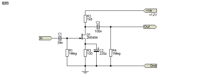
By measuring JFETs before use, you know what voltage range you need for the desired drain current. Because the parameter spread is so large, you need to design each JFET amplifier based on the measurements you take. No other amplifying device requires this step. To complete this example, we'll test a 2N5484 (I'll use the simulator, but I have run tests on 'real' JFETs too).
VGS (off) = -1.255V
IDSS = 3.37mA
The value obtained for VGS (off) is within the range given in Table 1 (-0.3 to -3.0V), and IDSS is also within the range (1 - 5mA). Another (seeming identical) device will almost certainly be quite different from the one you just tested. This is quite normal with JFETs, hence the need for an easy way to test them.
| JFETs are normally operated in the 'saturation' region, which is to say that the device will draw the maximum current possible for a given gate (negative) voltage. This doesn't mean that changing the drain voltage won't affect the current, because it will. The amount of change depends on the JFET itself, and (like all parameters) it will vary from one device to the next - even of the same type. The maximum current is defined by IDSS, the current drawn with zero gate-source voltage. That's why Table 2 shows the manufacturer's test voltage, which varies from one device type to the next. It should be apparent that expecting to operate a JFET with an IDSS of 1mA with a drain current of more than 1mA won't work - ideally the quiescent drain current will be somewhere between 50% and 85% of the rated (or measured) IDSS for minimum distortion. This isn't always possible. |
Now we can look at a design for the JFET just tested. We need to choose a drain current, and fairly obviously it must be less than 3.37mA because that's the maximum possible drain current, obtained with zero volts between the gate and source. While the current can be increased, that requires that the gate is driven positive with respect to the source, and this should be avoided in a linear circuit. A reasonable current would be a bit under half the maximum, so we'll settle for 1.5mA as an initial test. Since that's pretty close to half the maximum, we can try a negative bias voltage that's close to half the voltage measured for VGS (off), which gives us -625mV. The drain voltage (no signal) should be about 6V.
In the design shown (as well as the other examples that follow), an input capacitor is optional. The gate voltage is nominally zero, and an input cap is only necessary if the source has a DC offset. If present, the DC offset will disturb the bias point and the circuit may no longer work. The value of the input cap is determined by the gate resistor (R1) and lowest frequency of interest, usually 20Hz. The value should be 5 times that indicated by the usual formula ... C = 1 / ( 2π·R·f ). A value of 39nF is fine with a 1MΩ input impedance.
The important thing to note is that if you increase the value of R3, that increases negative bias, reduces JFET current, and in turn increases the drain voltage (due to the reduced current through R2). The converse also applies of course. The optimum drain voltage is half the supply voltage, with a suitable offset to account for the source voltage. Don't expect to get much more than 2V peak from a circuit such as that shown without significant distortion!
Since (at least initially) we are primarily interested in the DC potentials, no input signal is used. When power is applied the drain and source voltages can be measured to see how close we get to the original design figures. These are determined as follows ...
RS = 625mV / 1.5mA = 416Ω
RD = 6V / 1.5mA = 4k
These aren't standard values, so we'll use 390Ω and 3.9k. Remember, this is a first attempt, and we shouldn't expect it to be right first time around. The simulator gives the following values, which aren't too bad for a first guess ...
ID = 1.225mA
VGS = 495mV
VD = 7.2V
We can also measure the gain, as it's then possible to calculate the transconductance. There really isn't much point, but it's worthwhile for a better understanding of the JFET being used. The source resistor causes degeneration (as is the case with a BJT design), but JFETs don't have very high gain, so while we'd expect a gain of ten from a BJT, with the JFET it's only 5.2 (for a BJT in the same configuration, the gain would be [almost] RD / RS).
To measure transconductance, RS must be bypassed by a capacitor with a reactance of RS / 10 at the lowest frequency of interest. For good response at 20Hz, that means a 204µF cap - we'll use 220µF as it's a standard value. With the capacitor in place, the gain is 10.7 (20.6dB).
Transconductance (aka gm ['adopted' from valve terminology] or gfs - forward transfer conductance) is determined by dividing the change of drain current by the change in gate voltage. A gate voltage change of 10mV gives a drain current change of 29.2µA, so gm is 2.6mS (or 2.6mA/ V). The datasheet for the 2N5484 claims 3,000µmhos (3mS) to 6,000µmhos (6mS), so again, we're probably close enough (it varies with drain current amongst other things). The datasheet chart for transconductance indicates that with 1.2mA drain current, it should be around 2.5mS at 25°C.
Note: I do hope no-one thought that these parameters weren't affected by temperature - JFETs are no more immune to thermal changes than any other semiconductor.
This basic technique will work most of the time, but will only give acceptable biasing conditions if you know the actual values for VGS (off) and IDSS. If you work from averaged figures in the datasheet it will probably work, but it won't be optimised. Of course, the simple way to do the design is to select a 'suitable' drain current (that's well within the range shown), calculate the drain resistor, and use a trimpot to adjust the source resistance to get the maximum undistorted output from the drain.
gm = ΔID / ΔVGS (Δ means change)
The change of gate voltage should be kept small to ensure that non-linearity doesn't mess up the measurement. The change of drain current should be such that you can ignore it compared to the quiescent (no signal) current. Every time you use a different drain current, you'll measure a different transconductance, even on the same JFET. The curve is not linear, but tends to be parabolic, following what's generally referred to as a 'square law'. This can be defined by the following formula ...
ID = IDSS × ( 1 - [ VGS / VGS (off) ] ) ²
You don't need to remember this, as (like all JFET parameters) it varies. However, let's do an example, using the same JFET as before (2N5484), but we'll use the datasheet minimum IDSS of 1mA as our maximum, so quiescent current should be 500µA. For a 12V supply, we expect around 6V across the drain resistance, so by Ohm's law that works out to be 12k. This should work with any example of a 2N5484, and we'll simply use a trimpot instead of a source resistor. Based on the previous design exercise, the drain resistance is about four times the previous value (12k vs. 3k9) so the source resistance should also be about four times that used in the previous example. That means ~1.2k so a 5k trimpot gives plenty of adjustment capability. There's no need to be exact when a trimpot is used.
We end up with the circuit shown above. To get 6.7V at the drain (with ~820mV at the source), TP1 will be set for 1.8k (in the simulator), and the value of C1 can be reduced since the resistance is lower (the calculated 56µF cap is likely to be unobtainable, so you'd use 100µF). The gain without C1 is about ×5.1, and with C1 in place it's ×19.7 (25.9dB). The transconductance has changed too, and is reduced to 1.79mS. From this you can (rightly) deduce that transconductance does not imply the gain from a circuit, as the first example had a measured gfs of 2.92mS, but had lower gain!
In general, operating any JFET at a higher current will usually result in lower distortion, but you also get lower gain if the drain load is resistive. As noted, the drain current must be less than IDSS or you may cause gate current to flow, causing distortion (valves are no different in this respect). Recommendations vary widely, but my suggestion is to stay within 50% to 85% of IDSS for most circuits. Some circuits may perform better at higher or lower current, depending on the output amplitude. You also achieve the maximum output swing by using the Figure 3.2 circuit, although distortion will be quite high (> 1% is typical) if the output level is more than ~500mV RMS. Modifying the bias point is likely to make this worse, not better.
Input impedance is roughly equal to the value of R1, but it's frequency dependent. The input impedance is affected by input capacitance (CISS) and any gate leakage current. Input impedance is always higher at low frequencies, where the input capacitance has negligible effect. The output impedance is (again roughly) equal to the value of the drain resistor (R2). It's actually in parallel with the drain resistance (equivalent to plate resistance in a valve), but the drain resistance is normally very high and can be ignored. Remember that the drain resistor is also in parallel with the external load resistance (shown as R4), and if the load is low impedance, you'll lose voltage gain. The JFET 'sees' the combined resistance of R2 and R4 in parallel as its effective drain resistance, and this affects the gain. These caveats apply to all JFET amplifiers, regardless of topology.
In some designs you may see a voltage divider used at the input (gate) which is claimed to allow the JFET to operate over a wider range. While this may be true, it's far easier to use a trimpot, as this removes the likelihood of supply noise being coupled to the input, and it means that the input capacitor is optional if there's no DC present from the signal source. Even if you do use a voltage divider as shown above, you'll still need to use a trimpot or select the JFET. Distortion performance is not changed compared to the Figure 3.2 version.
If you don't include the source resistor bypass capacitor (C2), the signal to noise ratio (SNR) will be reduced. The resistor makes noise (see Noise In Audio Amplifiers for details), and this will be amplified by the JFET, acting as a grounded gate circuit for noise voltage at the source. C2 bypasses this noise and increases the gain, and the circuit will always have better SNR with C2 in place than it will without it. This isn't always possible or desirable, but you need to be aware of it.
Section 5 covers active load arrangements, but the one shown next is actually a better choice. The circuit is simple, and it has no issues with stability because the DC conditions are set with resistors, and not active devices. This happens because the 'current source' is only active for AC, and it does nothing at very low frequencies or DC. Once the trimpot is set to get symmetrical distortion and/ or clipping, it biases itself like any other simple JFET amplifier, but has exceptionally high gain. The bootstrap section involves Q2, C2, and the centre-tap of R2 and R3. Output impedance is low (only a few ohms) so the JFET isn't affected by the next stage's input impedance.

The bootstrap circuit ensures that the voltage across R3 doesn't change, therefore the current through it doesn't change either. This is a constant-current drain load, that gets the maximum possible gain from the JFET. My simulation says that the gain is ×100 (40dB), which is very good indeed for a single amplifying device. It's far higher than you'll ever get with a JFET in a 'conventional' circuit such as those shown above. Distortion performance is disappointing, with the simulation showing 2% at 1V peak (700mV RMS) output. This is obtained with only 10mV peak input!
The source bypass capacitor (C1) is optional, but if it's omitted the JFET will amplify the noise from R4 (trimpot). The gain variation is less than 3dB with it connected/ disconnected. Active current-source loads are discussed in Section 5, and while the theoretical advantages are clear, the practical realisation of an active load is difficult. The benefit of the scheme shown above is that the gain for DC remains small (around ×4.5 for the example shown), so setting up the DC operation parameters is no more critical than for any other simple JFET amplifier stage.
Earlier on, I mentioned using a servo around a JFET to set the operating conditions to the same drain voltage, regardless of the JFET used. The idea is quite valid, but is also silly - adding an opamp to a JFET circuit makes no sense, as you can just use the opamp to amplify. It will have predictable gain, lower distortion and much better performance than any JFET. However, we shall not let this deter us. 
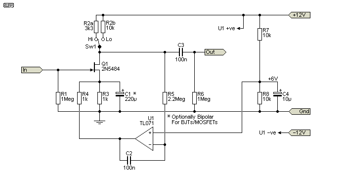
Sw1 (Hi/ Lo) lets you select the drain current so that low-current devices can be tested. In the 'Hi' position, the drain current is 1.82mA, reduced to 600µA in the 'Lo' position. Some JFETs will only work satisfactorily with drain current below 1mA. You can change the value of R2a/ R2b to suit your requirements. The tests described were all performed using the 'Hi' setting.
As you can see, this a completely over the top for a simple JFET amplifier circuit. The opamp uses ½ the supply voltage as a reference, so the drain of the JFET will always be at exactly 6V with a ±12V supply. The only case where it may fall down is with a FET with much higher than normal VGS (off), where the opamp's output can't swing far enough to compensate. With a J111 in circuit, the opamp's output voltage was +7.4V, needed to force the source voltage to +4.6V (-4.6V negative bias referred to the gate). The supply voltages should be a minimum of ±12V. The negative supply is only used for the opamp, so it can apply negative correction where required (this will be the case with low VGS (off) devices, where the 1k resistor would result in too much bias). With the simulator's 2N5484 in place, the opamp's output is -3.73V, with -48mV at the source of Q1 (yes, it's very slightly reverse biased).
If I use a J113 in my simulation, the output of U1 is -72mV, with the source voltage for Q1 then set to +871mV. The current through R2 never changes with no signal. Because the voltage is fixed at half the supply voltage by the servo (6V for this demo), the drain current is always 1.82mA, regardless of the JFET used. It's highly unlikely that anyone else will build this circuit, not because it doesn't work, but because it's not sensible to throw so many parts at a simple JFET amplifier stage. Note that C2 is optionally a bipolar electrolytic capacitor, only necessary if you wish to test BJTs or MOSFETs, as the emitter/ source voltage will be negative. For testing only JFETs it will be a standard polarised electro as shown.
For what it's worth, the circuit shown will work with an NPN BJT or a small-signal N-Channel MOSFET just as well as a JFET. Provided the opamp can provide sufficient voltage to bias the device used, it can be used to make direct comparisons between devices. I'm not entirely sure that this is useful, but some people may wish to put one together just for the fun of it. It's not often that you see a circuit that will automatically bias almost any device you choose to try. I measured the transconductance of a BC550C BJT in the same circuit, and it managed 22mS - significantly higher than any JFET and the 2N7000 MOSFET (13.7mS). The BJT had significantly lower distortion than the JFET or MOSFET. Testing PNP or P-Channel devices will require the circuit to be rewired to suit.
Some readers may choose this arrangement to quantify JFETs into categories in much the same way as the Figure 2.1 circuit, but providing the ability to measure gain as well as the required source voltage for operation at the selected current. For anyone often working with JFETs, this could be an invaluable tool. Maybe it's not quite as silly as I first thought!
The basic idea shown here is now available as a project, with plenty of detail so you can adapt it for your tests. See Project 237 for all the details. Test results are also presented, and it's the best JFET tester I've used.
The transconductance measurements are based on using the device in its intended mode of operation, and may not agree with the value stated in the datasheet. The figures quoted are usually based on a constant drain voltage and at a specified drain current. This almost certainly will be at a voltage and current that are different from the values you will use, and the figure will be different.
Figure 3.4 shows a bootstrapped drain load, which makes the JFET's drain current almost constant. As with BJTs and valves, using a current source load improves performance, usually resulting in higher gain and better linearity. When using JFETs, the simplest (although this may be debatable) is to use a second FET as the load, configured as a current source. JFETs aren't particularly wonderful in this role, but they are a simpler solution than a BJT current source. While the performance of the latter is a great deal better than the JFET, it's also more complex. A JFET needs just one resistor, as shown below. This will only work with well-matched JFETs.

If the JFETs are matched, the voltage across each will be close to identical, and the circuit will bias properly. With unmatched JFETs, you are in for a world of pain - unless the characteristics of both are close to identical the circuit will not work as expected. Perhaps surprisingly, the source resistor bypass capacitor (C1) makes very little difference to the gain. Depending on the JFETs used and operating conditions, it may increase the gain by between 3dB and 6dB, but that's all. Omitting C1 reduces distortion, and the degree can be significant (as much as 10:1). However, you may experience an increase in noise levels, as the resistor (R3) noise will be amplified.
An alternative is to use a current sink load on the source pin. This uses more parts, and looks like it would offer superior performance. However, the JFET doesn't really care how its drain current is defined, so an active or passive source circuit should make no difference. A simulation shows this to be the case, and both frequency response and distortion are almost identical. Note that there's no actual difference between a current source and current sink - it's merely a matter of semantics, not circuit behaviour. I haven't shown a circuit for this, as there's really no point.

This arrangement might appear to be ideal, since it provides much higher gain than any other variation. However (and you just knew there would be a down-side), it is extraordinarily sensitive to the value of R3 in relation to R2. Even a tiny parameter variation (such as will happen to the JFET with temperature) throws everything out, and it will either distort or may even stop amplifying altogether. The gain is ×222 (47dB), reduced to ×136 (42.6dB) without C1. Distortion is reduced by a factor of 2.7 if C1 is omitted. Interesting, but not useful in a 'real world' amplifier without a servo circuit (Figure 4.1). While that will work (very well) it's starting to get very silly indeed. All that for a JFET amplifier that still can't beat a couple of opamps!
Any active current source load will make the setup of DC conditions very difficult. This is because the JFET is forced to have extremely high gain for all frequencies including DC, so it's inevitable that even small changes (due to time and temperature for example) will cause large changes to the DC conditions. The simple way around this is to use bootstrapping instead, as shown in Figure 3.4. The loss of performance is measurable, but the circuit will actually perform better if the DC conditions are made less critical.
Having examined constant current, now we can examine constant voltage. The arrangement shown isn't one that I've seen, but it's inevitable that it has been used before. The opamp is used to 'current load' the JFET's drain, and (for an ideal opamp) there is (close to) zero AC voltage at the opamp's inverting input. The opamp obtains its reference voltage from the same connection (the JFET's drain terminal), and while it may seem unlikely that this will work, it does work very well. The opamp must have a high input impedance, and a FET-input type is recommended. However, due to the biasing scheme used, you can use a bipolar opamp (R3 should probably be reduced to around 100k).

Because of R4, which applies feedback and makes the inverting input a 'virtual earth' stage, the opamp has an input impedance of close to zero ohms. Biasing is provided via R3, and is bypassed with C3. C2 ensures that the opamp's DC gain is unity, to prevent serious offset problems. The opamp is wired as a transimpedance amplifier, meaning its output voltage is directly proportional to the input current (but inverted). The gain of the opamp stage is determined by the transconductance of the JFET and R4, and R2 only affects the gain by varying the transconductance a little. As simulated, the overall gain is ×23, and it can be increased or reduced by increasing (or decreasing) the value of R4. As shown, you'll almost certainly need to use a trimpot in place of R3 so the operating conditions can be set for the JFET you have (the value was 1k for the simulation).
There is almost zero voltage variation at the drain of Q1, so the only thing that changes is the current through the JFET. Since the voltage across R2 doesn't change, nor does the current through it. This arrangement sets up the JFET to operate as a 'true' square-law device, and it has only 2nd harmonic distortion. There is a tiny amount of 3rd harmonic distortion but it's 100dB below the fundamental. The 2nd harmonic is at -34dB, with a THD of just over 2% with 810mV RMS output (50mV peak input). The gain is directly proportional to the value of R4, so if it's doubled, so is the circuit gain. The JFET is operating with a transconductance of 2.23mS.
This circuit doesn't even approach 'ordinary'-if, and it most certainly is not hi-if. However, some experimenters might like to play with it, and it will be found that 2nd harmonic distortion is not as 'nice' as claimed by so many, because it still generates intermodulation distortion. Intermod is particularly troublesome with complex musical passages due to the vast number of additional frequencies generated. Having said that, I tried it as a guitar preamp, and it had plenty of gain with R4 set to 33k, and can drive a power amp directly. It tested much better than the simulation, and sounded great. However, it's still not hi-if.
Source followers (aka buffers) are intended to adapt high impedance sources to lower impedance loads. Unlike an opamp buffer, they always have a measurable voltage loss, so gain is typically around 0.9 rather than unity. There's no practical limit to the input impedance, but it will rarely be more than 10MΩ for most common designs. Although the gate current is small, it's not zero, so you must expect a small DC voltage to appear across the input resistor (R1). When properly designed, most source followers will elevate the gate to some positive voltage, so an input capacitor is mandatory (unlike the other circuits shown above).
A JFET source-follower has one significant advantage over a BJT emitter follower, in that the input impedance is not affected by the load (Note 1). Likewise, the output impedance isn't affected by the signal source (another odd characteristic of emitter followers). However, the output impedance of a source follower is nowhere near as low as that from an emitter follower. In this case, it's 330Ω, and while it's close to the same value as TP1 in this example, the two are not related. You must also remember that output impedance has nothing to do with a circuit's ability to provide current to a load. In a circuit that draws around 1.2mA from the supply, the maximum negative current will be less than 1mA, after which it will clip the negative half-cycles (a circuit such as Figure 7.2 is assumed).
¹ This isn't strictly true, because if you rely on bootstrapping to increase the input impedance, the following load reduces the output level. As the level is reduced, bootstrapping becomes less effective.
While it is (sometimes) possible to use a JFET with nothing more than an input and source resistor, mostly this gives woeful performance. The source will be at a voltage determined by the JFET's characteristics, which generally means the voltage is quite low (a little less than the VGS (off) voltage). With the 2N5484 I've used for other examples, the source voltage may only be around 700mV, and that is the absolute limit for a negative-going input signal. If the amplitude is greater than 1.4V peak-peak, the negative half-cycle will clip and the positive half-cycle will draw gate current. Distortion will be high even before clipping, so this is usually not an option. An example is shown below - this is not the way to build a source-follower!

Provided the input signal is less than 100mV RMS or so, the circuit shown will work, but it's just wrong, and has almost no headroom. Even with a mere 100mV input, the distortion is more than 0.5%, where it should be less than 0.01%. Fortunately, it's not at all difficult to get it right, with the addition of one resistor and an input capacitor. The requirement to know the specific values for VGS (off) and IDSS is just as important for a source follower as it is for a common source amplifier.
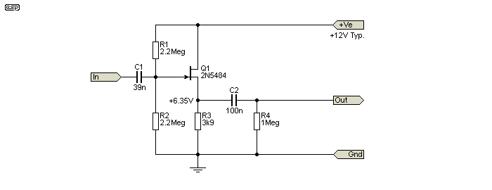
You'll See this used, but it's not the best example of design. The input impedance is 1.1MΩ, but of course R1 and R2 can be made higher values. However, having a resistor tied to the supply rail makes it susceptible to any supply noise. It also misses an important improvement that is provided by the next circuit. It is easy to set up, and will 'self-bias' quite well as long as R3 is a suitable value. 'Suitable' in this context means that it should pass no more than 85% of the minimum IDSS figure shown in the datasheet. The source voltage will be slightly higher than the gate, as required to bias the JFET properly. If R3 is too low in value, the input will draw gate current, which will cause distortion with high impedance sources. I used 3.9k, which will pass around 1.6mA (quiescent) and is a reasonable compromise between drain current and output drive capability.
In the following drawing, the values for R2 and R3 are the same as that shown in Figure 3.1 (390Ω and 3k9). Again, as a first guess (and based on the same calculations), it's pretty good. however, distortion performance is not quite as good as that for Figure 7.2. This also depends a great deal on the JFET used, so distortion figures are intended as a rough guide only.

The Figure 7.3 circuit (when set up properly) can handle an input of 10V P-P (3.54V RMS) with distortion below 1%. That's by no means wonderful, but at lower voltages (e.g. 1V RMS) it falls to around 0.17%. This is still pretty poor, and we need a more complex topology to improve it any further. It may come as a surprise, but bypassing R2 with a capacitor (220µF or so) actually increases the distortion, but has very little effect on the output impedance.
There's an unexpected change to the input impedance with the Figure 7.3 circuit. Because R1 is effectively bootstrapped (from the junction of R2 and R3), the input impedance is not 1MΩ as you'd expect, but is raised to over 6MΩ. If the input voltage is 1V, the voltage across R1 is only 160mV, implying an input impedance of 6.25MΩ (by calculation). The simulator also shows the input impedance to be 6.25MΩ, so input impedance has been increased by a factor of more than six. This isn't usually considered, but it's quite real. When R2 (trimpot) is bypassed as discussed above, input impedance is increased further, but over a limited frequency range.
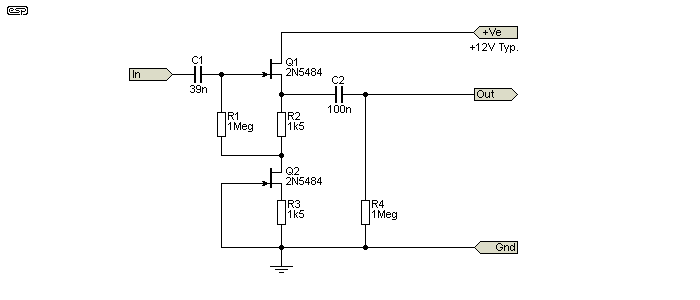
Much better performance is obtained by using a second (matched) JFET as a constant current sink, in the source circuit of Q1. For convenience, I used the same values shown in Figure 5.1, just rearranged to make it a source follower instead of a common source amplifier. Distortion (at 1V RMS) is reduced to 0.0039%, output impedance is around 550Ω and it's about as good as you can reasonably expect without a buffer stage.
Because the bootstrapping of R1 is more effective due to Q2, the input impedance has increased to over 70MΩ. However, it falls off as frequency increases, and is 'only' 5.4MΩ at 30kHz. In my simulation, the input impedance starts to fall beyond 1kHz, but it's unlikely that will cause the slightest problem in use. If you need very high impedance at low frequencies, this is the circuit you need. Unlike the 'standard' arrangement shown in Figure 7.2 which has an output level of 923mV (for 1V input), the Figure 7.3 circuit's output is 995mV. This is still less than unity gain, but it's close enough for most purposes.
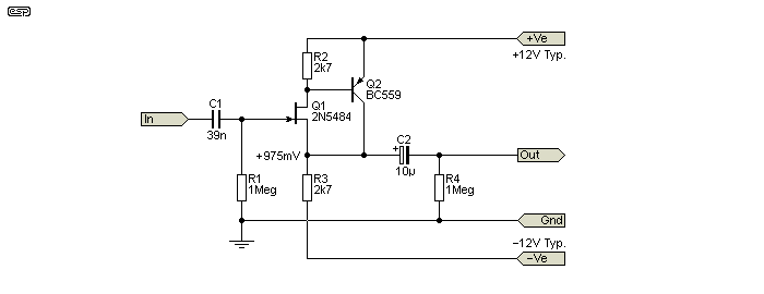
If you have a negative supply available, biasing a JFET follower is a great deal easier. You don't have to worry about the bias at all, as it looks after itself. You do lose the bootstrapping of course - it can still be done by adding another resistor and capacitor, but isn't shown here. The circuit shown can be used with just the JFET - simply leave out the transistor and replace R2 with a direct connection to the positive supply. Do not leave R2 in the circuit without Q2 - the circuit doesn't work properly if it's in place. Omitting the BJT from the circuit increases distortion and output impedance, and also reduces the gain to ~0.93 (vs. 0.99 with the BJT).
The BJT gives you the best of both worlds - high input impedance and a commendably low output impedance. The circuit shown has an output impedance of only 4Ω, but obviously cannot supply any useful current into such a low impedance. There are several variations on this theme, and it is preferred over a single-supply circuit. The values for R2 and R3 aren't critical, but need to be selected to suit the IDSS of the JFETs being used. The circuit shown can normally handle an input voltage of around 4V RMS with vanishingly low distortion. The addition of Q2 dramatically improves performance, reducing distortion by up to two orders of magnitude, a significant advantage.
The biggest limitation to extended frequency response is due to the gate-drain capacitance (CGD) and the Miller effect. The effective capacitance seen at the gate is equivalent to CGD multiplied by the AC voltage gain. Because most JFETs are symmetrical, the value provided for CISS is the sum of CGD and CGS, although some datasheets also provide different values for 'on' and 'off' conditions (particularly for switching types such as the J11x series). However, the gate capacitance is not a fixed value, and it varies with gate, drain and signal voltage (and of course between different JFETs - even of the same type).
Provided the source has a relatively low output impedance, the effects of input capacitance are negligible. However, when a JFET is used with a high impedance signal source, you can easily run into problems with poor high frequency response. Depending on the application, the only solution available may be to use a JFET as a source-follower before the amplifying stage. This negates CSG completely (as it's effectively bootstrapped) leaving only CDG which is referred to the supply rail. The 2N5484 that I used for many of the examples here has a CISS of 5pF, so you have 2.5pF for both CDG and CSG. As an amplifier with a gain of 21dB, the -3dB frequency is 159kHz with a 100k source impedance. This is extended to over 1MHz for a source follower under the same conditions.
Given that the Miller effect multiplies the gate-drain capacitance by the voltage gain, you might expect that the -3dB frequency should be much lower than the simulator calculated, but the Miller effect does not necessarily give an exact figure because the JFET's capacitance varies with drain current. However, you can prove it for yourself by adding external capacitors (around 1nF is a good value to try), and you'll find that CGD is indeed multiplied by the voltage gain.
At the time of writing I don't know if I need to provide diagrams to demonstrate this or not, so I've chosen not to include them. If readers want me to add the necessary diagrams I'll do so, but rest assured that the effects are completely real. Whether or not the input capacitance causes anyone any grief depends on the application, and for most audio applications it's usually not a consideration. However, be warned that switching devices such as the J11x series perform far worse than JFETs designed for amplification. Unfortunately, these are the very ones that are now the hardest to obtain.
One thing that you don't want is gate current, as this can lead to serious distortion. It's far less common with JFETs than valves that draw grid current, but it can cause the same problem, known as 'blocking'. This problem is almost always due to heavy overdrive of the stage, where the input signal's peak amplitude is greater than the FET's gate diode voltage. For this reason, it's not a good idea to use a JFET stage for a guitar distortion circuit, unless you ensure that it's properly configured to prevent blocking. If you don't include an input capacitor (C1 below) you will never have an issue with blocking, but if the preceding stage has a DC offset, then C1 must be included. Other measures may then be necessary to prevent blocking.
To achieve the blocking state, all that's needed is a transient input level high enough to forward-bias the gate diode. This causes the input capacitor to charge, which forces the gate voltage to become more negative. If the input signal is at a high enough level and from a relatively low impedance, when the level returns to 'normal', the JFET remains cut-off, and only a distorted remnant of the signal gets through until the gate voltage has returned to zero. The drawing shows a simulated circuit that works quite well. The distortion is fairly high, but that wouldn't be an issue with a guitar preamp for example. (Note that the JFET and/ or source resistor [R3] would need to be selected.) As simulated, the quiescent DC level on the drain is about 8V. This is higher than the ideal, but it's still within reasonable limits.
Fortunately, although blocking is likely with many configurations that are commonly used, it isn't a problem unless there's an input capacitor and the likelihood of high-level input transients that cause severe overload. With no input cap (or with a high impedance signal source) it's highly unlikely. That is not to say that it can't occur, as shown in the following simulation. For the first 4ms, the signal is at a 'normal' level (at around 460mV peak, 330mV RMS), and is amplified as expected. After just a 6ms burst of high-level (2V peak) the input capacitor (C1) charges to -1V. When the input returns to its previous level, the output is highly distorted, and shows a significant DC level shift. The circuit is fairly conventional, but is not optimised. Any JFET stage (with an input capacitor) can be forced into blocking, although it's usually not quite as severe as the waveform shown below.

The graph shown is directly from the simulator, and with an input voltage of ~330mV RMS it has a gain of ×22.5 (22.6dB). When the signal level is raised to 1.4V RMS, the gate voltage is driven to -1V via the gate diode, turning off the JFET. The high-level signal still gets through, but the amplifier clips heavily. Once the signal is returned to its former value, the JFET remains off until C1 discharges. With the values shown, this will take close to 50ms. While recovery is fairly fast, the sound is dreadful.
The blocking effect isn't necessarily limited to the JFET stage itself. In the waveform, you can see that the output voltage shows a significant positive swing, and this may cause the following stage to saturate (clip) until C3 discharges. The rate of discharge is determined by the input impedance of the next stage (rarely just a simple 100k resistor as shown), and while it may be fairly brief, it can still cause gross 'non-harmonic' distortion. This distortion is non-harmonic because it's based on a crude timer that is not affected by the input frequency. Complete blocking of a JFET stage is not necessary to cause problems with the following stage(s). A momentary bias shift may be all that's needed to cause havoc.
Note that this simulation deliberately makes blocking more severe than you are likely to experience with most designs. The example shown has been exaggerated for clarity.
Blocking isn't something you come across often, but when it happens, unless you know the cause, it may take some time to track down. The symptoms are obvious if you know what to look for, but if you've never come across it before, it can be difficult to work out what's happening. I came across it first about 50 years ago, when a colleague couldn't work out what was wrong with a valve amplifier that cut out after a brief transient overload. It could take up to 30 seconds before it would produce sound again, but most cases only involve very brief blocking behaviour (which sounds awful). You have to know what to look for! Once learned, problems like this are forgotten at your peril. Even blocking lasting a few milliseconds is enough to cause what should be guitar 'fuzz' to sound like 'fart'. As a guitar effects pedal, no-one has ever longed for a fart-box (to my knowledge at least. )
You'll often see JFETs used for muting. They are ideal in this mode, because by default the JFET is turned on (shorting the signal to ground) with no power, and when a suitable negative voltage is applied to the gate, the JFET turns off, and lets the signal through. The following is taken from the article Muting Circuits For Audio, and is shown again here because it's relevant.
Junction FETs (JFETs) can also be used, and like the relay they mute the signal by default. To un-mute the audio, a negative voltage is applied to the gate, turning off the JFET and removing the 'short' it creates. Unlike a relay, JFETs have significant resistance when turned on. The J11x series are often used as muting devices, and while certainly effective, the source impedance has to be higher than with a relay. The typical on-resistance (RDS-on) of a J111 is 30Ω (with 0V between gate and source). The J112 has an on-resistance of 50Ω, and the J113 is 100Ω (the latter is not recommended for muting). I tested a J109 (which is better than the others mentioned, but is now harder to get) with a 1k series resistor, and measured 44dB muting, and that's not good enough so two JFETs are needed as shown.
Note that JFETs will generally not be appropriate for partial muting (for a 'ducking' circuit for example), because when partially on they have significant distortion, unless the signal level is very low (no more than around 20mV), and/or distortion cancelling is applied. This application is not covered here.

To un-mute the signal, it's only necessary to apply a negative voltage to the gates. There is no current to speak of, and dissipation is negligible. JFETs are ideal for battery powered equipment, but there has to be enough available negative voltage to ensure that the JFET remains fully off ... over the full signal voltage range. If you use a J111 with a 10V peak audio signal, the negative gate voltage must be at least -20V (the 'worst-case' VGS (off) voltage is 10V), and the gate must not allow the JFET to turn on at any part of the input waveform.
Using a JFET to get a 'soft' muting characteristic works well. The JFET will distort the signal as it turns on or off, but if the fade-in and out is fairly fast (about 10ms as shown) the distortion will not be audible. You may be able to use a higher capacitance for a slower mute action, but you'll have to judge the result for yourself. I tested the circuit above (but using a single J109 FET) and the mute/ un-mute function is smooth (no clicks or pops) and no distortion is audible. Measured distortion when the signal is passed normally is the same as my oscillator's residual (0.02% THD).
If a JFET has an on-resistance of 30Ω, the maximum attenuation with a 2.2k source impedance is 37dB. This isn't enough, and you will need to use two JFETs as shown to get a high enough mute ratio. This is at the expense of total source resistance though. With the dual-stage circuit shown above, the mute level will be around -70dB. It is possible to reduce the value of the two resistors (to around 1kΩ) which will reduce the muted level to around -60dB, which is probably sufficient for most purposes. An alternative is to use two or more JFETs in parallel. Two J111 FETs will have a total 'on' resistance of 15Ω, four will reduce that to 7.5Ω, etc. Consider that a set of electromechanical relay contacts will have a resistance of a few milliohms!
You can improve the attenuation by applying a small positive signal to the gate, but it should not exceed around +400mV. Any more will pass DC through to the signal line as the (normally reverse-biased) gate diode conducts. In general I would not recommend this, as it adds more parts that have to be calculated for the mute control circuit, and the benefit isn't worth the extra trouble.
There is also the option of using a JFET based optocoupler (the datasheet calls it a 'symmetrical bilateral silicon photo detector') such as the H11F1. These are claimed to have high linearity, but I don't have any to test so can't comment either way. According to the datasheet, low distortion can only be assured at low signal voltages (less than 50mV). They might work as a muting device, but the FET is turned off by default, and turns on when current is applied to the internal LED. This means that the internal FET would need to be in series with the output for mute action when there's no DC present. The on resistance of the FET is 200Ω with a forward current of 16mA through the LED. I don't consider this to be a viable option.
Analog Devices used to make ICs called the SSM2402 and SSM2412 that included a three JFET 'T' attenuator and a complete controller circuit for a two channel audio switching and/or muting circuit. They have been discontinued, and there doesn't appear to be a replacement. They were aimed at professional applications such as mixers and broadcast routing, and would be useful parts if still available.
It would be easy enough to include the design formulae that are shown on many other sites that cover JFET design, or to show graphs that allow you to determine the optimum bias point for the device you plan to use. Unfortunately, these are pretty much redundant because every device you use will be different from the others in your parts bin - even of the same type and manufacturing batch. Unless you measure your JFETs and put each into a separate bag marked with the two main parameters (VGS (off) and IDSS), every design is pretty much a lottery.
This doesn't mean for an instant that I don't like JFETs, or that they should not be used. Apart from anything else, they can be quite good fun to play with, and they are ideally suited to applications that require a high input impedance. While most of the desirable JFETs are now difficult to obtain, they are still available from some major vendors, albeit with a reduced range. If you are willing to use SMD parts the choice is a little better, but these are hard to work with in experimental 'lash-up' circuits. RF (radio frequency) types are usually a little easier to get than the 'traditional' audio devices that were the mainstay of so many early designs, but these work perfectly at audio frequencies.
Using a trimpot to set the operating conditions (which may need to be altered to get maximum undistorted output level) is by far the easiest, but that still doesn't always mean that the design is optimal. The extreme variability of JFETs means that you either need to accept that every simple amplifier you build will be slightly different, or the circuit will be far more complex than almost any other solution. This is not the case if the input level is so small that the output swing needed remains (comparatively) tiny compared to the supply voltage, but it becomes an issue when the input level (and output level) are both high enough to create significant distortion.
The decision to use a constant voltage at the drain (as shown with Figure 6.1) or constant current (Figures 5.1 and 5.2) is easy. A constant current load gives the best performance and lowest distortion, but is usually very difficult to bias properly. So much so that unless you use a dual matched JFET, the chances of it behaving itself are fairly slim. This is solved by using bootstrapping as shown in Figure 3.4, which also provides a low output impedance. Constant voltage is more predictable and quite stable, but distortion performance is usually mediocre at best.
Contrary to what some people may claim, JFETs are not linear. For a given gain and output swing, a simple BJT stage will nearly always beat an equally simple JFET stage hands down. This is very much dependent on signal level though, and at low output levels (typically less than 500mV), a JFET may have lower distortion. Of course, this also depends on the JFET itself, the signal level and the supply voltage. Distortion performance of JFETs (and BJTs) can be improved dramatically by using a constant current source in place of a drain (or collector) resistor (as shown in Figure 5.1), but that's not always feasible with JFETs (parameter spread strikes again).
A common claim is that due to a JFET's square law behaviour, it is capable of producing only the second harmonic, with no higher order harmonics at all. While this is true, it generally only happens under very specific conditions that may not be achievable in your circuit. The conditions can be met, with the output being drain current modulation with the voltage unchanged (Figure 6.1). Unfortunately for those who may believe that this is somehow 'musical' or 'pleasant', it's not always easy to achieve with any realistic (i.e. usable) circuit. I can think of other ways it might be able to be exploited as well. What I can't think of is why anyone would bother. Such a circuit will still create intermodulation distortion, which is far more objectionable than the harmonic distortion that causes it.
Another furphy is that complementary JFET circuits (using N and P-Channel JFETs) are actually complementary. Having looked at the parameter spread of only N-Channel devices, it's obvious that getting perfectly matched complementary JFETs will be somewhere between extremely difficult and impossible. This would mean that not only are the JFETs of each polarity matched, but their opposites are matched to each other as well. That would mean identical VGS (off), IDSS and transconductance for N-Channel and P-Channel devices. This is very unlikely indeed.
All things considered, JFETs are useful when you need very high input impedance, along with wider bandwidth than you can get with (affordable) opamps. You do need to be aware of the gate-source capacitance (CISS) though, as that is often high enough to cause premature high frequency rolloff with high impedance sources. As a means of 'general purpose' or 'pure audio' amplification, JFETs should be one of the last choices after other possibilities have been exhausted. Wide parameter spread, lack of availability of good amplifying types, and limited gain means that JFETs should only be used when you have no other choice - this is rare for audio, but there are a few cases where a JFET is a sensible choice. JFET input opamps are usually a different matter, as some are very good indeed (the TL07x series are 'utilitarian' examples). It's worth noting that JFET opamps claiming 'superior audio performance' are engaging in hyperbole (or wishful thinking) - this is 'marketing speak' and doesn't necessarily represent reality!
One thing you may wish to experiment with a is symmetry. Because the 'default' bias setting is for ½ voltage at the drain, the output will almost certainly clip asymmetrically. If your overall level is well below the clipping level this isn't an issue, but if the JFET is used such that the output clips (in a guitar preamp for example), you will almost certainly get a better result if the bias is adjusted for symmetrical clipping. The idea that guitar amps are preferred to have even-order distortion (especially 2nd harmonics) is generally false, as it generally doesn't sound 'nice' at all.
By including a trimpot in the source circuit as suggested, you can easily adjust it until the onset of distortion is symmetrical. As the input is increased, simply adjust the trimpot until the top and bottom of the waveform are clipped (more or less) equally. Perfect symmetry is usually impossible because of the way the JFET works, but you can get close. You might imagine that adjusting for symmetrical clipping will power distortion at levels well below the maximum, but this will probably not be the case (it may be JFET dependent). The following test circuits were used to demonstrate the voltages expected. While the simulation uses BF256 JFETs, the same (or very similar) results will be obtained with any JFET.
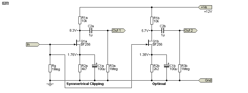
You can see that the only change is to the source resistance. To get symmetrical clipping, the value is increased to 4.7k, boosting the drain voltage to about 8.3V and source voltage to 1.76V. The 'optimum' circuit has a drain voltage of 5.7V and a source voltage of 1.38V. Despite the source bypass cap, the gain with symmetrical clipping is ×12.5 (22dB) and 'optimum' is ×15 (23.5dB). Distortion is 1.62% (symmetrical) and 1.04% ('optimum') for an output of ~425mV (35mV RMS input).
Where the signal will remain below clipping at all times, there's no real reason to aim for symmetry, as it will increase distortion (albeit slightly). However, you have the choice, and by including a trimpot instead of a fixed resistance for the source, you can adjust the circuit for any condition you like (including making it non-functional). The latter is unlikely to be useful as an amplifier though. Depending on the drain resistance, you may need to use anything up to a 10k trimpot to be able to get the desired operating conditions.
The gain of the circuit depends largely on the transconductance of the JFET, but is also influenced by the drain resistance and the following load impedance. Varying the source resistance (and therefore the drain current) affects both gain and distortion, as described above.
This section was added in 2026, largely due to a JFET preamp I had to build and my experiments with it. I figured that it was interesting enough to add the info here, in the hope that it will assist others who are experimenting with JFET stages.
You need to be careful with some references, as the claims may not stand up to scrutiny. Despite claims, JFETs don't sound 'better' than BJTs or opamps in well designed circuits. There are three main things that affect sound quality - frequency response, noise and distortion. Some of the latest opamps will beat any discrete circuitry in all three categories when properly implemented, and absolutely do not somehow 'mangle' your audio in ways that cannot be explained (without resorting to snake oil).
Main Index
Articles Index
