
|
| Elliott Sound Products | Part 3 - Active Power Factor Correction |
 Main Index
 Lamps & Energy Index
If you haven't done so already, please read Part 1 of this series first. There are many basic concepts that you need to understand, and it would be silly to repeat the information in Part 1. There will be some duplications, but only as needed to make sure that what you read here makes sense.
In many places I have discussed active power factor correction (active PFC), and it's about time that I explained the principles and benefits of the technique. Off-line - direct to the AC mains - switchmode power supplies (SMPS) have been with us for many years now, with the best known example being the standard computer power supply. For a long time, these have presented an awful load to the mains supply, drawing current only briefly at the very peak of the AC mains waveform. This applies to both desktop and portable PCs, as well as many other external supplies used in their millions worldwide.
Small switchmode supplies are used for all types of electronic lighting - compact fluorescent and LED lamps. CFLs in particular are made to a price, and power factor correction is very rare. I've examined a great number, and only came across one (one single, solitary example) that even made an attempt at including PFC. It was a simple passive design, so if you want to know how that works, see Part 2. Many of the better LED lighting fittings have changed to power supplies using active PFC, particularly those above 10W or so. This generally doesn't apply to retrofit globes, although there are exceptions there, too.
It's not possible to discuss every sub-class of active PFC, because there are too many, and the differences are mostly subtle. You may come across terms like CCM (continuous conduction mode), TM (transition mode) and DCM (discontinuous conduction mode), as well as other acronyms for the same things, and/or additional sub-classes. While the operational mode can make a big difference to the ultimate performance of a design, they all share (at least at the time of writing) the same basic concepts.
This article discusses the basics of active PFC, and is not intended as a design guide or as a reference text. There is a surprisingly large amount of information on the Net, including manufacturers' application notes for their PFC ICs, datasheets and white papers. Not all information is useful - especially if you don't understand the basic concepts.
The power supply circuit shown below is based on an application note by ST Microelectronics [1], and uses the L6562 IC - it's a mere 8 pin device, and seems to be quite unassuming, but the performance is excellent. The resulting circuit is considerably more complex than a simple rectifier followed by a capacitor (or a pair of caps in series as shown in section 1). However, it has an extremely good power factor, and is just one of many similar devices made by most of the major IC manufacturers.
In common with 99% of power factor correction circuits, the basic topology is a boost regulator, but with some extreme cleverness applied to ensure that the total current waveform is as close to sinusoidal as possible. The output voltage is always higher than the maximum peak voltage available from the mains, and 400V is a common choice. It can be lower, but cannot be lower than the AC peak voltage - that would require a buck/boost regulator, and would be far more complex. Most operate over a voltage range from 85V RMS to 265V RMS without any voltage range switching.
The pin descriptions are important to understand the operation ...
In order to describe the circuit properly, I have numbered various sections to make reference easier. We start with item 1, which is just a simple diode rectifier. Note that EMI filters have not been included, nor has the DC-DC converter section. These are required regardless of the topology of the rectifier circuit (and that's really what the whole circuit does). Note that there is only a small capacitance directly across the rectified AC - 470nF in this case. This cap is not for energy storage, but to ensure the remainder of the circuit is stable.
Next in the lineup is Item 2. This is a signal feed to the IC, so that the internal circuitry always knows the instantaneous voltage, which varies from close to zero to the peak of the AC waveform, either 100 or 120 times a second. The two 750k resistors are used to ensure that the voltage rating of each is not exceeded, and you see the same arrangement used in two more places as well.
Item 3 (2 x 180k resistors) is there to provide a voltage for the IC so it can start. Normally, power is derived from a winding on the main inductor (7), but this needs the IC to be operating before a 'proper' supply voltage is available. Directly related to this is Item 4 - a very basic power supply that's used to keep the IC functioning once it's started. The supply voltage is maintained at 18V by the zener diode. Although technically the inductor really is an inductor, it becomes a transformer due to the second winding that's used to power the IC and provide inductor current information to the controller.
Item 5 is the feedback network (which includes the 2 x 750k resistors and the 9.53k resistor). It tells the IC that the output voltage is correct, and includes capacitor networks to ensure phase stability so the output voltage doesn't 'bounce' up and down. This part of the circuit is quite critical, despite its apparent simplicity. The voltage regulation ensures that the MOSFET and inductor current is only ever exactly what's needed to keep the voltage stable at 400V DC.
Next is Item 6, the MOSFET. This simply shorts the end of the inductor to common, and causes a current build-up in the coil (7). At a time determined by the actual voltage present and the MOSFET/inductor current (monitored by Item 8), the MOSFET switches off again, and the voltage on the MOSFET's drain rises to 400V (regardless of the input voltage, but with some limitations), forward biasing the diode (10) and flowing to the load and filter capacitor (11) via the NTC thermistor.
A boost regulator relies on the energy stored in the inductor, and when the switch (MOSFET) turns off, there is a flyback voltage that is determined by the load current and stored charge. The IC must monitor every parameter - input voltage, inductor and MOSFET current, as well as the output voltage.
As discussed briefly above, the active PFC circuit is a highly evolved boost regulator. But, how does a boost regulator work anyway? The boost regulator is so fundamental to the operation of PFC circuits from many, many manufacturers, it's worth a brief description of the basic topology. This description is based on the constantly varying supply ranging from zero to the AC waveform peak. For more information on basic SMPS concepts, see the Switchmode Power Supply Primer.
The only real difference between a 'standard' boost regulator and a PFC booster is in the ability of the PFC IC to instantly compensate for the input voltage variation, and this is done inside the chip itself. Most data sheets provide quite a bit of information about how they work and their benefits. Of course, every maker claims their device to be better than the rest for one reason or another.

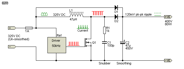
The general idea is shown above. The oscillator runs at 50kHz, so has a period of 20µs. The MOSFET is turned on for a very short period, and the inductor current rises from zero to (say) 4.5A during that period. When the MOSFET switches off, the voltage rises to 400V, and the inductor supplies the load and recharges the 47uF capacitor. The inductor current can be seen to fall from the peak down to zero over the next 3us. The 1k resistor and 100pF capacitor form a snubber network, which damps oscillation caused by the leakage inductance of the inductor and stray capacitance.
D1 may appear redundant, but it's often very important, although it's not always necessary. While it theoretically just bypasses the inductor when power is applied, it also prevents resonance due to L1 and C2. This is an 'unexpected' event, but it's very common with 'choke input' filters, which this circuit is until the MOSFET starts switching. The resonant circuit can cause the voltage across C2 (and Q1) to be much higher than the typical 400V that's obtained when the circuit is operating normally. ¹ The maximum voltage that can be developed depends on the inductance and capacitance, as well as the point on the AC waveform where the mains is switched. If the values all just happen to be 'worst-case', a peak voltage of up to +50% can be obtained (325V can be boosted to 487V).
¹ The above information was provided by Rice Technology LLC, and I thank Dave Rice for the information. This is something that I'd not seen discussed before.
Many of the commercial ICs designed for active PFC operate with a variable frequency. This helps to spread the high frequency noise over a wider bandwidth (but reduces the quasi-peak value at any given frequency), and also allows the IC to change its mode of operation on the fly to maximise efficiency and maintain the best possible power factor. The 'Ref' input to the controller allows it to adjust the duty-cycle to ensure that the current waveform is not distorted.

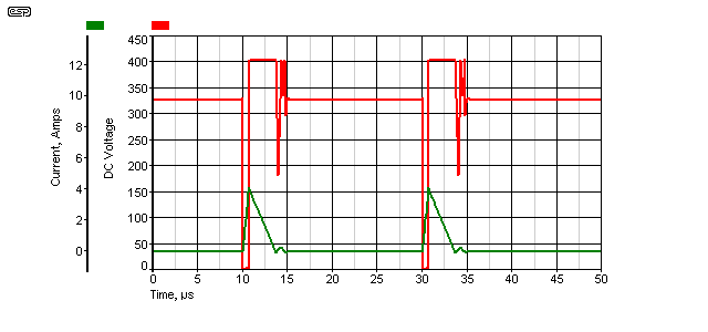
The waveforms for the switching cycles are shown in Figure 3. When the MOSFET is switched on, its drain voltage falls to zero (close enough), and current flows through the inductor, rising linearly as seen. The drain voltage can be seen to start at 325V (the applied voltage), and when it switches off, it rises to 400V and stays there for about 3us. After that, the stored energy in the inductor is depleted, and the voltage returns to 325V ... after a period of oscillation (which is damped by the snubber network).
Should the load current increase or input voltage decrease, the MOSFET needs to be switched on for longer, and conversely, if the load current falls or input voltage rises, the on time will be reduced. There are many ICs available that are suitable for boost regulator circuits, but they expect a reasonably steady input voltage. It can (and will) vary, but over a comparatively small range.
For an active PFC circuit, the MOSFET's on time is constantly adjusted as the input voltage changes, such that the inductor stores the same energy regardless of the instantaneous input voltage. This is the task of the PFC chip - it needs to be able to track the input waveform in real time, making adjustments for both the input voltage and load current. The ultimate goal is that the AC current waveform will be ...
In reality, there is almost always a discontinuity near the zero-crossing point of the AC waveform, and this looks just like crossover distortion in a power amplifier. The degree of discontinuity depends greatly on the design of the IC. The ST L6562 is particularly good in this respect - a point that's made in detail in the data sheet. The discontinuity is also affected by the input voltage and load current, and although any discontinuity does cause greater distortion of the current waveform, the power factor is usually not badly affected.
Compare this with the current waveform of the capacitor input filter circuit seen in Part 1, where very high peak current is drawn, but only at the very peak of the AC waveform. Distortion is extremely high (typically well in excess of 100%), and the power factor is so bad that the circuit draws almost twice as much current as an equivalent circuit with unity power factor.
The circuit shown above is just one example, but was selected because the schematic is easy to follow. For lighting in particular, there are several ICs designed to perform all the functions needed for a complete solution. The active PFC and DC-DC converter functions are combined into one device, simplifying the overall design. The converter shown below is a flyback type.
The above is shown as a conceptual example. Essentially, one IC controls everything, providing both PFC functions and LED current regulation. There are component values shown, but they are examples derived from the application note. Everything you need to know is available should you have the burning desire to design a LED lighting power supply. Please see the data sheet for an explanation of the pin designations.
The way the MOSFET is driven is very different from most driver ICs. There is a low voltage MOSFET in the IC that switches the drain of the external device, and that's why the gate of the external MOSFET is bypassed by a capacitor. Because of this, the IC is limited to relatively low power applications, but you'd need to look a the application note (e.g. SLUU478) to get more information about the configuration and typical component values for a 13W supply. Note that in this supply as well as that shown in Figure 7, the 'Common' connection is not protective earth. The secondary of the circuit (the LEDs and current sensing) may be connected to earth if desired, as that part of the circuit is fully isolated by the transformer - provided it is a suitable type made to the applicable standards.
 |
The Y2 capacitor shown (in subdued hues) between primary and secondary is usually required to meet EMI standards. Y2 caps are designed to be electrically safe - failure must never cause the secondary to be come live. These caps are common in most switchmode power supplies - personally, I think it's a really bad idea, but the EMI regulators will just state that electrical safety isn't their problem - it belongs to the safety regulators. I've been told this directly! I've seen examples of 'fake' Y2 caps used in imported supplies - some are just 3kV ceramic types (not marked Y2), but there are several reports of caps that are marked as Y2, but are no such thing. |
There are many other examples of integrated SMPS with PFC, and a Web search will find a vast amount of information. Much of it is not in a form that actually explains very much though, so it can be very time-consuming trying to track down useful data - I know this from my own searches to find material for this article and my own education.
Only a few years ago active PFC was considered to be 'high-end', with substantial additional cost involved, but I have seen 9W LED lamps that have active PFC built in. Government legislation already exists for some product categories, and these must meet or exceed a prescribed minimum power factor or they cannot be sold. Expect to see this applying to more products over the next few years.
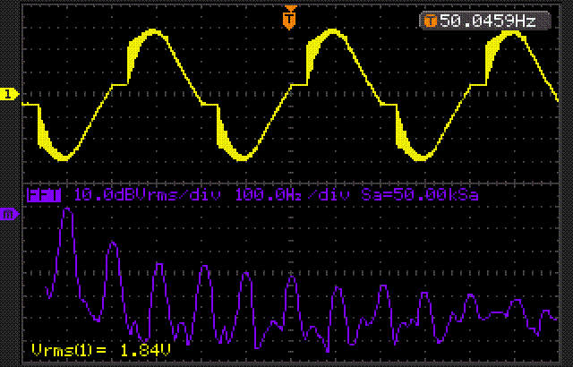
Fortunately, my lab setup is such that I can test and record measurements of waveform distortion, harmonics, inrush current (I had to design and build my own tester for that - see Inrush Current Testing Unit) and many other things that savvy customers want to know before purchase. The captured waveform shown below is an example of a power supply's current waveform when active PFC is used.

The above shows clearly that there can be a significant discontinuity at the zero crossing point of the waveform. It's unrealistic to expect the power supply to behave normally current with virtually no voltage to work with, but this is a rather extreme example, selected to show the problem clearly. The waveform is quite distorted, but still provides a power factor of 0.89 and the harmonic content is acceptable, with only the 3rd harmonic above -20dB. This measurement was taken on a 100W power supply running at 40W, with 230V mains derived from a lab sinewave power supply (used so that mains distortion did not affect the measurement).
It's worth noting that only odd harmonics are permitted above very low levels, because the presence of even harmonics signifies an asymmetrical waveform that has a DC component. Any power supply that imposes DC onto the mains will not pass compliance testing, because the effects have very serious consequences for the grid infrastructure and other users.

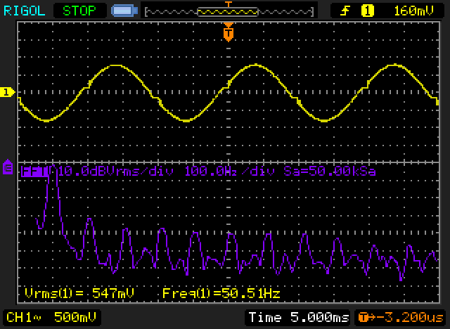
The best I have seen so far is shown above. This supply is a 125W power supply that draws an almost perfectly sinusoidal current waveform, with only a tiny discontinuity at the zero crossings. THD measured 2.5% (with mains supplied by my lab sinewave generator), and power factor was an impressive 0.98 - there isn't a trace of switching noise on the mains current. If this is the shape of things to come (and I believe it is just that), we'll see more power supplies that are so close to being a resistive load that any difference is academic.
I hope that this article has provided the reader with some insight into the inner workings of PF corrected power supplies. While the circuitry appears complex (and the design process is definitely not for the faint-hearted), the results are so good that most power supplies will have full PFC circuitry before too long. It's generally not worth the extra cost for small (less than 10W or so) supplies, but it is now common with LED lamps with a rated power as low as 12W.
With modern surface mount manufacturing, you get a power grid friendly power supply, that already provides a regulated output, so the converter design is simplified. Most will have some basic regulation for critical voltages (such as the 3.3V and 5V rails for computers), but the overall regulation scheme is greatly simplified by having a regulated voltage to start with.
These same manufacturing techniques also mean that the extra cost is minimal. Large electrolytic filter caps aren't needed, and that in itself is a saving. The ICs and MOSFETs are cheap, and the inductor (with its additional winding) is the most expensive part of the circuit. Regulatory bodies worldwide are beginning to insist that mains harmonics are minimised because of the problems they create within the power grid, and using a PFC supply is the only way to pass their requirements. Even well-informed customers have found the pitfalls of a poor power factor, and now ask some potentially embarrassing questions before they will purchase products (especially lighting).
I know this personally, as I've had to supply the answers to the questions. Fortunately, my lab setup is such that I can test and record measurements of waveform distortion, harmonics, inrush current, and many other things that savvy customers want to know before purchase.
So, that finishes a hopefully easily digested foray into the mysterious world of power factor correction circuits. Fortunately, most of the hard work has been done by the chip designers, and there's one thing that's certain - they wouldn't have gone to all that trouble if there was no market for their ICs. Active power factor correction is here to stay, and it will only get better as IC designers refine their circuits even further.
See 'Further Reading' below for some in-depth material. Naturally, IC makers will always use their own devices in application notes and 'handbooks', but the information provided is excellent in both suggested documents. Both go into considerable detail and have several demonstration circuits, but also have good introductory info as well.
A final comment is warranted here. While modern supplies with active PFC are very good, long-term reliability must also be considered. Many of these supplies cannot be repaired, not just because of the extensive used of SMD parts, but some are embedded in thermally conductive resin. Even where this isn't used, the designs are often so compact that many parts have to be moved (or removed) to gain access to the failed component(s). If a failed IC is no longer made, it's likely that the supply has to be scrapped anyway, and some of the ICs used have a short manufacturing life. The resources that are thrown away are considerable, but the trend is accelerating so don't expect a resolution any time soon.
 Part 1 - PFC Introduction
 Part 2 - Passive PFC
Further reading ...
 Main Index
 Lamps & Energy Index
| Copyright Notice. This material, including but not limited to all text and diagrams, is the intellectual property of Rod Elliott, and is Copyright © 2012. Reproduction or re-publication by any means whatsoever, whether electronic, mechanical or electro-mechanical, is strictly prohibited under International Copyright laws. The author (Rod Elliott) grants the reader the right to use this information for personal use only, and further allows that one (1) copy may be made for reference. Commercial use in whole or in part is prohibited without express written authorisation from Rod Elliott. |