

|
| Elliott Sound Products | Switchmode Power Supply Primer |
 Main Index
 Articles Index
Contents
The linear power supply is far from dead, but in commercial products switchmode power supplies (SMPS) and switching regulators have pretty much taken over. While the circuit complexity is far greater, there are significant savings to be made with the transformer in particular. Where a linear supply transformer needs to operate from 50Hz or 60Hz mains, the switching equivalent typically operates at 25kHz or more, so it's a lot smaller.
For regulators, the saving is in the heatsink. A linear regulator with an input voltage of 22V DC and an output voltage of 15V will dissipate 7W for each amp drawn by the load. For low currents this isn't a problem - a preamp power supply may only draw 100mA or so at most, so the dissipation will be 700mW and a small heatsink is all that's needed. At higher currents, the losses become far greater. With any linear regulator, the losses are dissipated as heat, and there is no way to get rid of it other than by using a heatsink.
A switching regulator will have far fewer losses, but more importantly, they also provide a transformation of input and output power. For example, if we assume for a moment that the switching regulator is 100% efficient (no losses at all), the power output must equal the power input. If the input voltage is 22V, output voltage is 15V and load current is 1A we can do a quick calculation ...
Power Output = Power input = 15W
Output current = 1A
Input current = 15 / 22 = 682mA
We have an output current that's greater than the input current. This is important, and compared to a linear equivalent represents a significant gain. Now, work out the linear regulator's loss if the input voltage is increased to 30V. We are still drawing 1A, so now the loss is 15W - 15V across the regulator and 1A output current. The input power is 30W, and half of that is effectively thrown away. Of course there are losses with a switching regulator, typically copper and core loss in the transformer or inductor, switching losses in the BJTs, MOSFETs or IGBTs, and power needed to run the controller circuitry.
The same thing applies to a full-blown 'off-line' (powered directly from the AC mains) SMPS. It can not only perform the power conversion with greater efficiency, but it can be designed to provide a fully regulated output as well. So, not only has the transformer size been reduced by a factor of 20 or more, but there's no need for additional circuitry to provide a regulated output.
It would seem to be an 'all-win' situation, but naturally that's not really the case. The SMPS operates at anything from 25kHz up to 150kHz or more and uses square-wave switching. As a result there is noise generated that extends well into the radio frequency bands (> 1MHz) and the DC output will also have noise superimposed on it. This noise is notoriously difficult to remove, and it can radiate a considerable distance, using the mains and DC leads as antennas.
However, switchmode supplies and regulators are here to stay, and the noise is something that we just have to deal with. This article explains the basics of how switchmode power supplies and regulators work. It's not a design guide, and it contains no project circuits for you to build. The intent is to provide a good explanation of how each type of circuit functions, because there is surprisingly little information available that isn't either highly technical or 'dumbed down' to the point where it's of little practical use.
| Linear | Switchmode | |
| Size/ Weight | Large/ Heavy | Small/ Light |
| Efficiency | 30 - 40% See Note | 70 - 95% |
| Complexity | Low | High |
| Design Skills Needed | Low - Medium | High - Very High |
| EMI | Low Noise/ Low Frequency | High noise/ High Frequency |
| Cost | Medium - High | Low - Medium |
Note that the efficiency of a linear supply shown in the table assumes it's regulated. For a transformer, bridge and filter cap unregulated supply, efficiency can be better than 85%, assuming a transformer rated for more than ~100VA. Small, low current mains transformers are notoriously inefficient though, and the table reflects that.
The table above shows the relative differences between a linear power supply or regulator and its switchmode equivalent. When switching supplies first started to appear, they were very expensive and the required parts were uncommon. All the parts needed are now readily available and comparatively cheap, helped along by the proliferation of SMPS and the need to get the highest efficiency possible. The latter has become an imperative as electricity prices have risen dramatically, and governments worldwide have imposed minimum efficiency standards to many products. Some of these are wide-ranging and divisive - the phase-out of incandescent lamps being a case in point. All 'new' lighting products (LED, CFL) use switchmode supplies.
The general principles described here are also applied in an area that you may not have expected - induction cooktops. These rely on a steel base in the saucepan, and energy that flows through the coils induces large eddy currents in the base of the pan, causing it to get hot. The switching devices operate at between 25kHz and 60kHz, and most use IGBTs (insulated gate bipolar transistors) for their high voltage rating and power handling.
In a switchmode power supply, eddy current losses in the core are undesirable, and most use ferrite cores because they have much lower losses than the silicon steel laminations that are used for lower frequencies. There are many formulations of ferrite, which is a ceramic material containing minute iron oxide and other magnetic particles, with each insulated from the other so that eddy current is much lower than would otherwise be the case. Ferrites used for SMPS applications usually have high magnetic permeability and high electrical resistance. All forms of ferrite are fragile and easily chipped or broken if mishandled.
The advent of switchmode supplies has brought with it a whole range of new terms, some of which are self-explanatory and many that are not. The following is not extensive, and covers the basics only. Where power levels are given, these are a guide only, and examples of much higher/ lower power can be found.
Buck Regulator One of the most common switching regulators. The output voltage is lower than the input voltage. Boost Regulator Another common switching regulator. The output voltage is higher than the input voltage. Buck-Boost Regulator Provides a fixed regulated output regardless of input voltage (at least within the design range). Output voltage is inverted. SEPIC/ Cuk Buck-boost topologies that use capacitors and inductors for energy storage. Flyback Simple SMPS topology, suitable for low to moderate power output (usually no more than 150W). Forward Converter Medium to high power SMPS (50 - 200W). Higher efficiency than flyback, but also more complex and costly. Push-Pull Medium to high power SMPS, up to 1,000W. Semiconductor switches are stressed by a voltage that's double the input voltage. Half-Bridge Medium to high power SMPS applications, typically up to 500W but often much more. Full-Bridge High power SMPS, from 500W up to the maximum possible for a given mains circuit (10A, 20A, etc.) 2kW and more is not uncommon.
Switch BJT, MOSFET or IGBT, depending on desired power level from converter and switching frequency. Duty Cycle The ratio of on time to off time for switching devices. A squarewave has a 50% or 1:1 duty cycle. Reset When applied to magnetics, this refers to a sequence that returns the core to a demagnetised state to prevent asymmetrical operation and/or saturation. PWM Pulse Width Modulation, used in all regulators and many off-line switchmode supplies. PWM changes the duty cycle. Galvanic Isolation This means there is no ohmic connection between primary and secondary. Some capacitive coupling will always be present. EMI/ EMR Electromagnetic interference/ radiation. Noise that may affect other nearby equipment and is difficult to filter out. CCM Continuous Conduction Mode - The magnetic flux in the transformer or inductor does not fall to zero from one switching (commutating) cycle to the next. DCM Discontinuous Conduction Mode - The flux in the transformer or inductor falls to zero from one commutating cycle to the next. Hold-Up Time The length of time the SMPS can provide normal operation after input power is disconnected (allows for momentary interruptions).
The above covers the most common circuit topologies and terminology, and topologies are discussed in a little more detail in the next section. Greater analysis will be performed later in this article, but we need to be acquainted with the basics first. Any discussion of magnetics (inductors and transformers) will be limited to a few basic parameters, as there is far too much involved to go into any great detail.
While most SMPS types use a controller IC to provide regulation and other 'housekeeping' functions (current sensing, soft start, protection circuits, etc.), in some cases the SMPS will be self-oscillating, and may use very crude techniques overall. In some cases this even extends to high power supplies used for large amplifiers and other applications where you might imagine that a few dollars extra would have been money well spent. For a simple boost regulator used in an LED torch (flashlight) you can accept that the cost will be kept to a minimum, but in other cases it would seem prudent to use a slightly more complex circuit to get the best performance. However, some high-power self-oscillating designs often work surprisingly well ... at least until they fail.
There are two SMPS projects on the ESP website. The first (Project 69) is a low power supply that's largely intended for people to dabble with a switching supply without breaking the bank. The second (Project 89) is designed to run power amps in a car from ±35V using the car's 12V supply (typically 13.8V when the engine is running). Both use the SG3525 controller - one of the few that has survived for any length of time.
The following circuits and descriptions are very basic, and only show the essential ingredients of each design. There will always be additional components used, not only for the control circuitry, but also resistor/ capacitor (or resistor/ capacitor/ diode) snubber circuits in parallel with inductors and transformer primaries. These circuits suppress high voltage spikes caused by leakage inductance. There will also be additional filtering for both inputs and outputs to reduce EMI.
Where a magnetic component (inductor or transformer) has more than one winding, the start of the winding is shown by a dot. All topologies using dual (or more) windings on a single core require that the primary and secondary are properly phased to ensure that the circuit operates as intended. If windings are not correctly phased, the circuit either won't work or will fail when power is applied.
Buck converter: One of the simplest, cheapest and most common topologies. This topology does not provide isolation between primary and secondary, but it is ideal as a DC-DC converter used to step down from a high voltage to a lower voltage. Typically has high efficiency, and works well at high power levels. The down side to buck converters is that the input current is always discontinuous, resulting in higher EMI. The buck topology only requires a single inductor.
Boost converter: Like the buck converter, non-isolating. The boost topology steps up the voltage, so the output voltage is greater than the input. The boost converter generally operates in continuous conduction mode (CCM). It is used in SMPS designs as an active power factor correction (PFC) circuit, and is also used to provide higher operating voltages for circuitry powered by 5V (such as USB devices).
Buck-boost: These converters can either step the voltage up or down. This topology is very common in battery powered applications, where the input voltage varies depending on the state of the battery. It has the disadvantage of inverting the output voltage, but if the source is a battery or some other form of floating supply this is easily corrected by reversing the source voltage's polarity. Buck-boost converters use only a single inductor.
SEPIC: Single-ended primary-inductor converter and Cuk (named after its inventor) topologies both use capacitors for energy storage, as well as two inductors. With SEPIC designs, the two inductors can either be separate or a single component in the form of a coupled inductor, but Cuk designs use two separate inductors. Both topologies are similar to the buck-boost topology in that they can step-up or step-down the input voltage, making them ideal for battery applications. The SEPIC has the additional advantage over both the Cuk and the buck-boost in that the output is non-inverting.
Flyback: These converters are essentially a buck-boost topology that uses a transformer for isolation and as the storage inductor. The transformer provides isolation by means of separate windings, and by varying the turns ratio the output voltage can be adjusted. Since a transformer is used, multiple outputs are possible. The flyback is the simplest and most common of the isolated topologies for low-power applications. They are well suited for high output voltages, but the peak switching currents are high. The flyback topology is not suited to output current above 10A.
One advantage of the flyback topology over the other isolated topologies is that many of them require a separate storage inductor. Since the flyback transformer is also the storage inductor, no separate inductor is needed. Because the rest of the circuitry is simple, this makes the flyback topology a cost effective and popular choice. Operating mode is discontinuous.
Forward Converter: Basically a transformer isolated buck converter. The forward converter is best suited for medium power applications. While efficiency is comparable to the flyback, it does have the disadvantage of having an extra inductor on the output and is not well suited for high voltage outputs. The forward converter has the advantage over the flyback converter when high output currents are required. Since the output current is non-pulsating, it is well suited for applications where the current is in excess of 10-15A, as a comparatively small output capacitor is needed.
Push-Pull: This topology is essentially a forward converter with a centre-tapped primary winding. This utilises the core of the transformer more efficiently than the flyback or the forward converters. However, only half the copper in the winding is being used at any one time, increasing the copper losses. For similar power levels, a push-pull converter will have smaller filters compared to a forward converter.
The main advantage that push-pull converters have over flyback and forward converters is that they can be scaled up to higher powers. Switching control is critical with push-pull converters, because 'dead time' has to be provided to ensure that both switches are never on at the same time. Doing so will cause the equal and opposite flux in the transformer, resulting in a low impedance and a very large shoot-through current through the switches, destroying them. Peak switch voltage is at least double the input voltage, and high voltage MOSFETs are required. Push-pull converters are common for converters that operate with relatively low input voltages (12V to 48V or so).
Half-Bridge: These converters can be scaled up well to high power levels and are similar to the forward converter topology. Half-bridge also has the same issue of the shoot-through current if both switches are on at the same time. The duty cycle is therefore limited to about 45%. The half-bridge switch voltage is equal to the input voltage, and this makes it much more suited to 250VAC and PFC applications.
Full-Bridge: These require four switches and fairly complex control circuitry. The full transformer primary is used, and like the push-pull and half-bridge the maximum duty cycle is limited to about 45% to prevent shoot-through current in the switches. Full-bridge converters are suitable for very high power and often use IGBTs rather than MOSFETs.
Resonant LLC: This is a half or full-bridge topology that uses a resonant tank circuit to reduce the switching losses. All switching is done with (close to) zero voltage across the switching devices. These converters scale up well to high power levels and have very low losses in the switching devices. They are not well suited for stand-by mode power supplies because the resonant tank circuit needs to be energized continuously.
The resonant LLC also has an advantage over both push-pull and half-bridge topologies in that it is suitable for a wide range of input voltages. The main disadvantages of this are its complexity, design difficulty and cost. However, it remains popular because the stresses on the switching devices are reduced.
While there are many variations on the above, the brief descriptions cover the important points. Not all will be covered in detail below, because this is an article, not a book. In every case though, the transformer or inductor is the heart of the circuit, and is the most difficult to design. High switching speeds mean that the skin effect becomes problematic - this is the effect where current migrates to the outer layer of the conductor. The core itself is also critical, and some topologies require a gapped core due to an effective DC component, while others do not. These topics will be covered in greater detail further on.
An important point to make is that inductors (including 'transformers' used for energy storage) store energy in the core as magnetic flux. Energy is not stored in the winding(s). Leakage inductance is a by-product of winding an inductor or transformer, and is almost always undesirable. PCB traces and other wiring also add inductance that can ruin the performance of a switchmode regulator or power supply. Leakage inductance is inductance that exists on both sides of the transformer, but the primary is the most critical. While it's added to the total primary inductance, its 'charge' is not transferred to the load and must be dissipated by a snubber network or clamp. It is the result of imperfect coupling between the windings and magnetic flux 'leakage'.

The drawing shows the equivalent circuit of a transformer. This is pretty much a 'universal' model, and almost everyone who discusses transformers will use a similar circuit. The model assumes that there is no saturation. This is a non-linear function that's very difficult to model accurately without dedicated software, and the closest most people get is to include a resistor (RP) to represent the core loss. Of particular interest as leakage inductance, as this causes voltage spikes in a switchmode circuit. Note that the 'ideal transformer' is lossless, and has no resistance or capacitance, and has infinite inductance.
A critical aspect of the design (and understanding) of switchmode supplies is the behaviour of an inductor when a voltage source is connected. Inductance causes the current to rise relatively slowly, so when the voltage is connected there is initially zero current, and it rises exponentially to a value limited by the internal winding resistance. All SMPS limit the time a voltage is applied across an inductance so that the current never has time to rise above the peak design value. As the frequency is increase, the amount of inductance needed is reduced.
It's also important to understand the difference between an inductor (even though it may have more than one winding) and a transformer. Transformers do not store energy - it is passed directly to the secondary as an alternating voltage. Flyback converters use a multi-winding inductor, and it is technically incorrect to call it a transformer because of this. However, energy is passed from the primary to the secondary via transformer action (due to the coupled inductors), so it's really a moot point. Most people will continue to call flyback inductors 'transformers' whether it's technically correct or not, and that includes me.
As noted above, when a voltage is applied to an inductor, the current builds from zero to some value determined by the inductance, applied voltage and time. For the waveforms shown below, the inductance of the choke or transformer is 200µH, the voltage is +12V (±12V for the transformer) and the frequency is 100kHz. A complete cycle takes 10µs. The duty cycle is 50% (5µs on, and 5µs off). Duty cycle may also be expressed as a number between 0 and 1, so 1:1 = 50% = 0.5 as an example.
Inductors are often used as a 'choke' - part of a filter circuit with a low-pass characteristic. When used this way, the output voltage is determined by the duty cycle of the input waveform. A DC input means that the input and output voltages are nearly equal, limited only by winding resistance. A perfect squarewave (50% duty cycle) means that the output will be half the input (a 0-12V squarewave gives a 6V output), and that's the first thing we'll look at. It's important to understand that the reactance of the inductor must be high for the frequency used. A 200µH inductor has a reactance of almost 126 ohms at 100kHz, and the load needs to be lower than that before the effect of the inductor is fully realised. The waveforms shown below were taken after steady state conditions were reached.
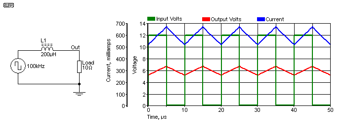
As can be seen, when the input voltage is at +12V, the inductor current (blue) ramps up, as does the output voltage. When the input falls to zero, the inductor current ramps down. Note that the inductor current never falls to zero - this indicates CCM (continuous conduction mode). The output voltage can be seen to vary between 5.4V and 6.6V, and the average is 6V - exactly as expected. The small diagram is indicative of the output filter that's used with most PWM switchmode supplies, but does not include the capacitor. The idea is to show what the inductor does by itself.
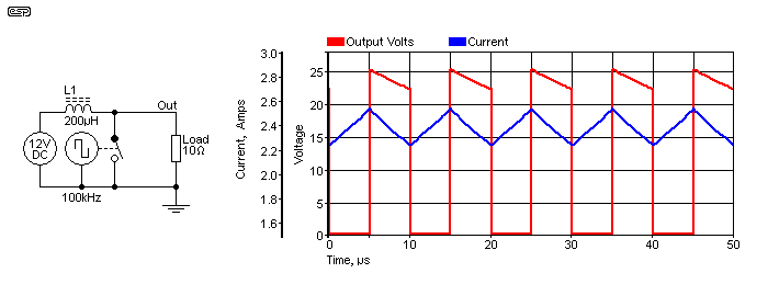
The flyback technique is very different in all respects. This is the arrangement used for boost converters and flyback SMPS. The input is 12V DC, and the other end of the inductor is shorted to earth/ ground via the switch. Again, the switching has a 50% duty cycle, and it's immediately apparent that the peak output voltage averages double the DC input. Although shown with a resistive load, it should be obvious that adding a diode and capacitor will maintain a voltage across the load that's higher than the DC input. Note that the average voltage across the load is still 12V, but the peak is double, at 24V.
When the switch closes, current again builds in the inductor, and the energy is stored as a magnetic field. When the switch opens again, the back-EMF from the inductor tries to maintain the same current through the windings. Because there is a load that absorbs energy, the magnetic field collapses and power is sent to the load. The incoming supply is 12V DC, so the flyback energy 'stacks' on top of the existing voltage, producing an average peak value of 24V. The actual average is 12V, and it only becomes useful if transformed (via a second winding on the inductor) or the peak value is used via a diode and capacitor.
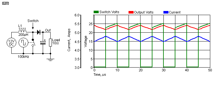
Now there is a diode and capacitor added between the inductor/ switch and the load. The flyback voltage from the inductor can now flow only one way via the diode. It charges the capacitor and supplies load current. The current waveform still behaves as before, but the average output current has now risen dramatically because all the energy stored in the inductor is being used by the load. To maintain balance, the current increases, and the output voltage is now (almost) double the input voltage. About 1V is lost across the diode.
Average current is 4.63A. and with a 12V input that equates to 51.6 watts. The average output voltage across the load is 22.5V, so output power is 50.6W with around 1W lost in the diode. You can see that the output voltage falls when the switch is on, and rises when the switch turns off again. Current behaves as expected, and as shown above.
These interactions with inductors are very important, and if you don't know what to expect then you don't have much chance understanding how switching regulators work. If at all possible, the reader should either build the circuits or at least run some simulations.
If you intend to build the boost converter test circuit shown above, the inductor should ideally be an air-cored type (such as a loudspeaker crossover coil). These can never give you a nasty surprise due to saturation, because air-cored coils don't saturate. They don't rely on a core at all. You will also need a fast squarewave generator, and a 555 timer configured as an oscillator will do fine. The frequency needs to be around 100kHz if you use a 200 - 220µH inductor. The switching device will be a MOSFET (IRF540 or similar) and you need a fast diode such as a MUR120 (200V, 1A). The load resistor will need to be no less than 47 ohms or the current will be too high (the 10 ohms used in the above examples was used for the graphs, and is not recommended for experimental circuits). Don't operate the circuit with no load, as the voltage will be too high for the capacitor (I've measured over 400V with no load while experimenting!). The maximum recommended load resistor is 1k, which will give an output of up to 50V with 50% duty cycle. Higher duty cycle (greater on time) means more output voltage.
There is an expectation that anyone building test circuits already has an understanding of basic electronic principles and experience with circuit construction.
Transformer waveforms are nowhere near as interesting as inductor waveforms, because a transformer simply transfers the input waveform to the output, stepped up or down based on the turns ratio. There is one example that is needed though, and that's an input waveform for push-pull, half or full-bridge SMPS circuits. The required switching waveform features a dead-time, when neither switch is on. The duty cycle of each switch is less than 50%, typically up to a maximum of 45%. The waveform and test circuit is shown below.
The waveform in Figure 4 is idealised - in reality it will be somewhat different because of the effects of the transformer's primary inductance, and it's also shown using an ideal transformer (having 'infinite' inductance, zero winding resistance and perfect primary-secondary coupling). As the inductance is reduced, the waveform changes and much of what you would see wouldn't make any sense. The principles don't change though. When Q1 turns on, that end of the winding is connected to earth, and the other end rises to +24V - this is simple transformer action. Conversely, when Q2 turns on, the other end of the winding rises to +24V. The peak-to-peak voltage across the winding is 48V.
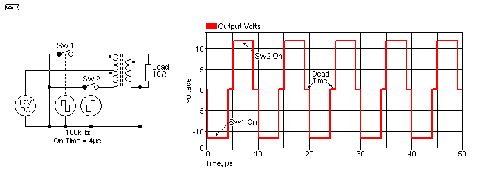
The period where both switches are off is called the dead time, and without it there is the possibility of both switches being partially on at the same time. This causes what's known as 'shoot-through' current, a brief current spike that can produce enough momentary current flow to cause failure of the switching devices. The dead time is included to ensure that can never happen, as it results in extreme dissipation in the switches and drastically reduced efficiency - at least until the switches fail. When both switches are on, the momentary current is almost unlimited. 100A or more is easily achieved even with relatively low voltage circuits, and limited only by circuit resistances.
Although it's not shown in the waveform above, the dead-time creates a problem with a real transformer, because it will have leakage inductance. This causes voltage spikes when each MOSFET turns off, and a snubber circuit is almost always necessary. The snubber is a deliberately lossy circuit, and the spikes generated are absorbed and ultimately dissipated as heat. This is energy that can't be delivered to the load, reducing efficiency.
One thing that is absolutely critical is the waveform symmetry with push-pull, half-bridge and full-bridge converters. These converters use a transformer that has no air gap, and if the drive signal is not symmetrical a DC component will appear in the transformer's primary winding. This will cause partial (and asymmetrical) core saturation, and the supply will (not may - will) blow up. The half-bridge is a little bit more forgiving because one end of the winding is capacitively coupled, and the cap(s) will equalise the voltage across the winding. However, if the drive is asymmetrical, the output will be too, and there will be more ripple as a result. Likewise, the windings must be symmetrical as well, with the same number of turns and winding resistance for any dual primary configuration.
A reasonable understanding of all the concepts seen in this section will be needed when we examine the basic circuits. In a switchmode regulator or power supply, a microsecond is a long time, and a fault lasting only a few µs can cause instantaneous failure. It can take a while before you get your head around the idea of such short timing sequences, but every test and experiment shown can be performed using a 1kHz switching circuit. What that means in the real world is that the size of the inductor and any filter capacitors increases dramatically, but the principles are unchanged. If you reduce the frequency by a factor of 100, then the inductance and capacitance needed increase by the same amount. It's easy to understand why high switching frequencies are used - everything is smaller and cheaper.
In the following descriptions, diodes will normally be either ultra-fast or Schottky. Standard diodes will fail, because they cannot turn off quickly enough. Schottky diodes have a lower forward voltage so dissipate less power. This improves overall efficiency. Switches may be BJTs, MOSFETs or IGBTs depending on power levels. The controller is simply shown as a 'black box', with a DC input, switch driver and feedback terminals.
The feedback applied to the controller is used to vary the duty cycle of the switch control signal. It's generally assumed that the switching frequency is constant, but that's not always the case. Sometimes the frequency is 'dithered' or modulated to spread the RF interference over a range of frequencies, rather than one fixed value. With the standard RF noise tests, this usually results in a lower level of EMI and a passing grade for a circuit that may otherwise fail conducted or radiated emissions tests.
In most cases, a longer 'on' time results in a higher output voltage, as this allows the inductor current to reach a higher level, thereby having more energy to transfer to the load. Squarewave inverters are not normally able to provide a regulated output unless there is an inductor in the secondary circuit, and the output waveform from the converter uses PWM. In some cases, regulation may be provided by an active power factor correction circuit that produces a constant regulated voltage to the inverter.
It's also common for SMPS to use 'hybrid' technology. One that's fairly common is to combine flyback and forward converter techniques to create what's sometimes known as a 'forward-flyback' topology, where the design utilises both techniques simultaneously. These are most commonly found in small supplies, with outputs of up to 30W or so.
In the circuits that follow (Figures 5 to 9) there is no galvanic isolation between the input and output. These circuits cannot be used where isolation is required. Figures 5 and 6 include component values and switching duty cycle, based on a 50kHz switching frequency. The inductor used for both is 220µH with a 1 ohm series resistance.
Component values are not shown for most of the remaining circuits.
We'll start with step-down (buck) switching regulators, because they are easier to understand and will help lead the way into more complex topologies. There are many different circuits, and a great many variations on each, so it's necessary to limit the discussions to the most common types. Of these, the buck regulator is one of the most common, and is used in wide variety of different products.
Figure 5 shows the essential elements of a buck converter. The switch is usually a PNP transistor or a P-Channel MOSFET because it's located in the incoming positive supply line. The switch can be located in the negative lead, but there's little to be gained by doing so. The output voltage is determined by the duty cycle of the switch. If it's on permanently the output is the same as the input (ignoring resistive loss in the inductor). Likewise, if the switch is off permanently, the output voltage will be zero.
At a 1:1 duty cycle (switch on for 50% of the time), the output voltage will be some fraction of the input, and input current will be less than the output current. The exact voltage is load dependent, and is also determined by the reactance of the inductor at the designed switching frequency. PWM is used to maintain the output voltage at the desired value. Buck regulators always operate in discontinuous mode.
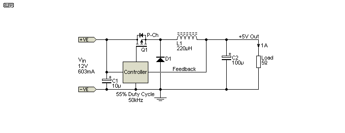
When the switch closes, current flows through the inductor to the load and filter capacitor. The control circuit will adjust the on-time to ensure that the voltage is always at the preset value. When the switch opens, the energy stored in the inductor's core is returned to the capacitor and load via the diode, ensuring that as little total energy as possible is lost. Without D1, a very high (flyback) voltage would be developed across the inductor which will destroy the switching device. With the designed load current, a boost converter will normally operate in continuous mode. It will enter discontinuous mode with no (or very light) load.
Losses in the switch, diode and inductor mean that the simplistic approach above does not hold true, but if the inductor is well designed the losses will be very low. Inductor quality is proportional to cost, so expecting a very low loss component means it will cost more. Diode losses are minimised by using a Schottky device, and switching losses depend on the type of device used and the switching speed. Overall efficiency is typically around 85%.
The component values and duty cycle shown are based on a simulation, and I've also run tests that validate the simulated results. The feedback will modify the duty cycle depending on the load, so if less current is drawn from the output, the duty cycle will be reduced to ensure that the voltage remains at 5V. Obviously, if the load is increased so too is the duty cycle. The average peak current will be around 1.1A with the conditions shown.
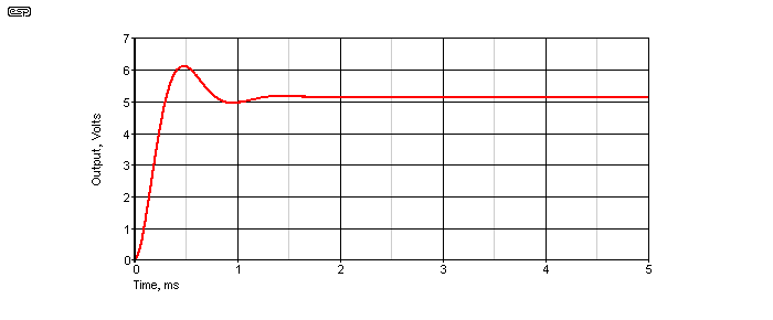
Something to be aware of with all choke input filters such as a buck regulator, or at the output of most PWM converters, is shown above. The output voltage waveform initially overshoots the design value, then has a damped ringing waveform at a relatively low frequency (this is very much load dependent). The frequency is determined by the inductance (220µH) and capacitance (100µF), which in this case is 1.07kHz. The overshoot is made worse by a light (or no) load, because there's nothing to damp the circuit.
If this isn't accounted for, the overshoot can easily damage sensitive components, so a soft-start arrangement is needed to gently ramp up the duty cycle when power is first applied. In the sections below, there are many SMPS that use this output filter, and all of them will show similar behaviour. The low frequency resonance also makes the feedback network more critical because there are phase shifts that must be accounted for to ensure a stable feedback loop.
The same effect can be seen with SEPIC and Cuk DC-DC converters. It may also occur with boost or conventional buck-boost designs operating in boost or buck mode, depending on component values, load and duty cycle.
Boost converters provide an output voltage that's higher than the input. This also means that the input current is higher than the output current by a ratio that depends on the step-up ratio of the converter. If the voltage is doubled, then the input current will be slightly more than double the output current. When the switch is closed, current builds up in the inductor, and when the switch opens the stored charge is dumped into the filter cap and load via D1.
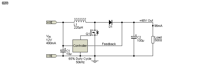
Boost converters rely on the flyback technique. The high voltage impulse developed when the switch opens is the load's source of voltage, which is effectively 'stacked' on top of the supply voltage. If the switch is permanently open, the load will get the incoming supply voltage, less the drops across the diode and inductor. The switch must never be allowed to close permanently, or a very high current will flow through the inductor, limited only by the resistance of the winding.
A common usage for boost converters is for active PFC (power factor correction) in switchmode supplies. The rectified but un-smoothed mains voltage is boosted to around 420V DC, with cycle-by-cycle PWM used to ensure that the input current is very close to being sinusoidal. The DC is then provided to a DC-DC converter to provide the voltage and current required by the load. Power supplies with active PFC can achieve a power factor of 0.95 easily (a PF of 1 is ideal). Active PFC is a highly specialised use for boost converters.
As with the buck converter shown above, the values shown are from a simulation and verified with bench tests. The peak MOSFET current is 1A for the conditions shown.
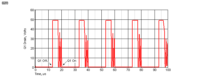
The waveform for a boost regulator is interesting, because it shows the flyback response clearly. The MOSFET is turned on for 13µs and off for 7µs, which gives the 65% duty cycle as shown. When the MOSFET (Q1) is on, the voltage across it is close to zero, and the flyback pulse rises to a little over 48V when Q1 turns off. This boosted voltage has sufficient current capacity to charge C2 to 48V, as well as produce the load current of 100mA. The peak charge current is 990mA, and the output ripple will be about 15mV.
The behaviour of a flyback SMPS (covered below) is not much different, but the voltages are a great deal higher for 'off-line' (mains powered) converters. The principle isn't changed though. The ringing you can see happens when there is not enough energy left to charge the output cap, but it hasn't fallen to zero. The voltage 'bounces' up and down a few times, but ringing is stopped when the MOSFET turns on again. The effect is load and duty-cycle dependent, and can happen with any flyback circuit.
The output voltage of a boost regulator can be anything from a few volts above the input supply, or can be hundreds of volts for low output currents. The MOSFET and diode must be able to withstand the full output voltage
The buck-boost topology allows the output voltage to be lower, higher or the same as the input voltage, but of the opposite polarity. The ratio of input to output voltage is determined by the duty cycle. When the reactance of the inductor and load resistance are the same, a 50% duty cycle means the output voltage is close enough to being the same as the input voltage, but reversed polarity.
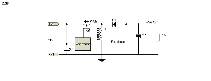
A high duty cycle (greater than 50%) causes the output voltage to increase (become more negative) and a low duty cycle does the opposite. If the incoming supply is from a battery the polarity inversion is of no consequence. By reversing the supply's output connections, the output voltage will be the desired 'normal' polarity. With the designed load current, a buck-boost converter will normally operate in continuous mode. It will enter discontinuous mode with no (or very light) load.
The voltage across the diode is equal to the sum of the input and output voltages. For example, with 12V input and -12V output, the diode's peak inverse voltage is 24V.
The SEPIC (single-ended primary-inductor converter) topology is useful when you need voltage step-up and step-down. SEPIC converters use a capacitor and two inductors for energy storage, and have slightly higher efficiency than the standard buck-boost circuit. It has the advantage of being non-inverting, but this comes at a cost because of the extra components. The two inductors can be wound on a single core (coupled inductors) or they can be separate. The SEPIC topology is unique, in that leakage inductance is actually a benefit. This eases the design process for the magnetics.
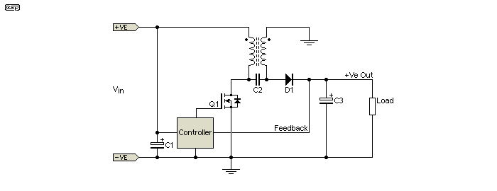
Although I've shown the coupled-inductor version, the inductors can be separate and even of different values. When coupled, the inductors will be equal values with the same number of turns on each section. Coupled inductor designs will typically provide an efficiency improvement over a separate inductor solution. The capacitor (C2) must carry slightly more than the full load current.
The operation of this type of converter is far more complex than those shown so far. It is often described as being equivalent to a boost converter followed by a buck-boost converter, but with both controlled by a single switch. While this may be a convenient way to describe it, it fails to provide a real understanding of its operation. However, that description will have to do, because I'm not about to provide many paragraphs and drawings for one converter. There's plenty of information on the Net of course, so look it up if you are interested.
This regulator is superficially similar to the SEPIC, but is quite different. For a start, the output voltage is inverted, having a negative output for a positive input. While it may appear that you only need to reverse the diode (D1) to get a positive output, this changes operation dramatically and its input current rises alarmingly. Like the SEPIC, the Cuk converter uses two inductors, and they are not usually coupled. The capacitor carries the full load current.

There doesn't appear to be any particular advantage of the Cuk over the SEPIC or vice versa, so the decision as to which one to use becomes the choice of the designer. Cuk converters do have the distinct disadvantages of requiring two separate inductors and having an inverted output.
There is a coupled inductor version of the Cuk converter, and a bit more info used to be available at boostbuck.com but the site has vanished. The main claim to fame of the coupled inductor version is very low (possibly zero) output ripple. It is specifically recommended for use in PWM (Class-D) amplifiers, although I've not seen an example.
This next batch of converters are commonly used following a bridge rectifier and high voltage filter capacitor, powered directly from the AC mains. These SMPS provide full galvanic isolation between the input and output, and are used where isolation is required. Y-Class capacitors are usually connected between input and output for EMI suppression. These caps must be certified, and are generally no more than 4.7nF to minimise the chance of electric shock.
However, the charge stored by even a 1nF cap is more than enough to damage sensitive circuitry, such as the inputs/ outputs of opamps or digital circuits. Many devices using an SMPS will not use the mains protective earth, so the output of the supply may float at around half the mains voltage. This can (and does) cause equipment failures, most of which will be considered inexplicable by the average user. More detailed analysis of the input stage and filtering is provided below.
As with the previous examples, the controller is simply shown as a 'black box', with a DC input, switch driver and feedback terminals. In reality, the controller will generally be a dedicated IC, although discrete transistors may be usable in some cases. Control circuitry is not included as part of this article, but may be provided in a later update if demand warrants a second article.
In some squarewave converter applications (push-pull, half-bridge or full-bridge) the output is unregulated, and the output voltage will change along with the incoming mains supply voltage. In such cases, the inductor on the secondary side is not used, and the filter capacitor(s) charge to the peak value of the secondary voltage. Filtering is comparatively easy, because the off time is short and the filter caps can be a fairly low value. However, any ripple on the incoming rectified DC is passed straight through the converter, so the high voltage filter capacitor (shown in Figure 16) needs to be substantial.
All diodes must be high speed types. For low voltages, Schottky diodes are recommended, and for higher voltages they must be fast or ultra-fast types designed for switchmode power supply use. The diodes will need to be mounted on a heatsink when appreciable current is expected. For example, with an output current of 5A, fast diodes will dissipate 4W each, and they will get very hot without a heatsink.
In each case, feedback is provided by an optocoupler (LED + photo-transistor) to maintain isolation between the primary and secondary sides. You will also see that only the secondary side is shown with an earth reference, because the input is referred to the mains and is decidedly user-hostile.
The flyback topology is probably the most popular switchmode topology of all time. It's not especially efficient, but is relatively easy to design and is ideally suited to small off-line SMPS (direct to the mains with a bridge rectifier). Flyback supplies are used almost exclusively in 'wall' power supplies (i.e. 'plug-packs', 'wall-warts'), and are very common for many other supplies used in lighting (mainly LED), battery chargers for phones, tablets and many laptop PCs.
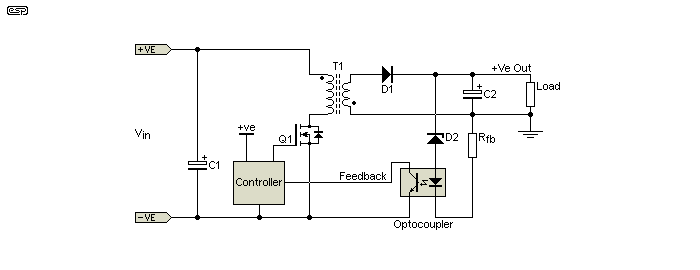
The flyback topology is based on the boost converter, but uses a transformer instead of an inductor. This allows the output to be fully isolated from the mains, and by manipulating the turns ratio, any output voltage desired can be achieved. Multiple outputs are common, with regulation usually based on the main output - the one with the highest power output. Flyback supplies are not common for output powers of more than about 100W because other topologies provide far better efficiency at high power levels.
When the switch closes, current builds in the inductor, creating a magnetic field. No power is supplied to the load while the switch is closed. When the switch opens, the back-EMF (the flyback voltage) transfers the stored energy into the load via D1. The normally very high back-EMF is clamped by the load, and is transformed by the turns ratio to produce the required output voltage. Note that the switch must never remain on, as that would represent almost a short-circuit across the supply.
The transformer requires an air-gap because there is an effective DC component in the transformer primary current. This also means that the transformer is somewhat larger than it would be without the DC component. The gap isn't always a physical piece of plastic or paper - it's not uncommon for flyback circuits to use a powdered iron core, where the 'gap' is distributed as microscopic spaces between the magnetic domains.
Voltage regulation is achieved by PWM. At no load, the switch will be on for a very short period, with the on-time increasing with increasing load. It's common to apply cycle-by-cycle current limiting to ensure that the primary current can never exceed the maximum allowed in the design. This provides automatic overload protection. Although not shown, a snubber network is (almost) always used in parallel with the primary to prevent voltage spikes caused by leakage inductance from damaging the switching device.
The forward converter is more efficient than flyback designs, and can be used at higher power levels. While the two look superficially similar, they are actually very different indeed. The first and most obvious difference is the second 'primary' winding. This is called a reset winding, and in conjunction with the diode it 'resets' the core to remove the DC component. The transformer does not require an air-gap. The reset winding is the one that has D1 in series, and has the same number of turns as the primary.
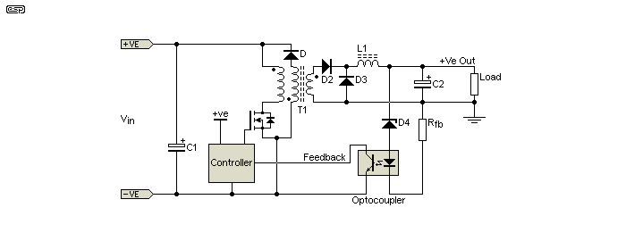
Power is transferred to the load when the switch is closed, and the core is reset by the separate winding when the switch opens. No power is transferred to the load when the switch opens, and the transformer is used as a 'real' transformer rather than an energy storage device. Because there is no energy storage in the transformer, a secondary inductor is required, and it forms a choke-input filter (these used to be common with very high performance valve circuits, although not common for audio amps). A choke input filter is a design exercise in itself, and forward converters require more design skills than flyback types.
Forward converters have a disadvantage over flyback designs in that there is a requirement for a second primary (reset) winding, and they need an inductor on the secondary side. Because the reset winding takes up space in the core's winding window, it's not possible to get very low primary resistance as the wire size must be reduced to fit the two windings. However, the output filter capacitor requirements are eased somewhat and forward converters can be built to operate at higher power than flyback.
Note that there are many variations on the standard forward converter, and they may use two switches and no separate reset winding, or the reset circuit may even be on the secondary side. It's not possible to try to list or show examples of every kind, because there are so many.
For medium-high power applications, the push-pull topology is useful. It's not especially efficient in its use of the winding window because there are two primary windings, and it has a disadvantage in that the switches (usually MOSFETs) have to withstand double the input voltage. When the mains is rectified and smoothed, the voltage is 325V for 230V mains, so the switches must withstand a peak voltage of more than 650V. Allowing for voltage spikes caused by leakage inductance and also for high mains voltages (typically up to 267V RMS), MOSFETs rated for around 900V are needed.
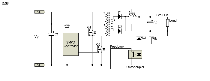
Power is transferred to the load when either switch is on, and it uses normal transformer action. The switches must be carefully controlled to ensure that they can never be on simultaneously, and it's usual to limit the duty cycle to each of them to no more than 45%. This provides a dead-band, where both switches are turned off. The disadvantage of this is that the collapsing magnetic field creates a back-EMF that cannot be completely absorbed by the load. Leakage inductance generates spikes that must be tamed with snubber networks, further reducing efficiency due to the power lost in the snubbers.
Regulation (if provided) relies on the use of an inductor in the secondary circuit, and the duty cycle of the switching waveform is varied. The output inductor then functions as a buck converter, with the PWM being applied to the primary of the transformer rather than in a secondary circuit. While shown with a centre-tapped secondary and two diodes, a single winding can be used with a bridge, or the output can be configured for dual outputs (e.g. ±40V for an audio power amplifier).
Many push-pull SMPS have been built that are self-oscillating (using small additional windings to provide feedback), and most of these do not provide a regulated output. As the mains voltage changes, so does the output voltage. The self-oscillating topology is simple and fairly easy to understand, but is hard to get right. Failure is usually catastrophic, as it's difficult to provide good protection circuitry yet maintain a low component count.
Push-pull converters can be seen to be similar to a push-pull valve amplifier's output stage, hence (at least in part) the name.
The half-bridge uses two switches, one to connect one end of the primary winding to the positive supply and the other to connect it to the negative supply. The other end of the transformer's primary is capacitively coupled to ensure that no DC component can exist in the winding. R1 and R2 are used to ensure the voltage across C1 and C2 is equal. The voltage applied to the primary is half the rectified and smoothed voltage, so with 230V mains, the primary voltage is about 162V peak, or 325V peak-to-peak. Since the applied voltage is somewhat lower than a push-pull design, the secondary windings require more turns, increasing the copper loss.
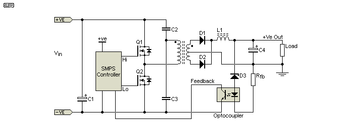
Power is transferred by normal transformer action when one or the other switch is closed. The controller must ensure that both switches can never be closed at the same time, or the shoot-through current will destroy the devices. The drive circuit is complicated by the fact that one of the switches is 'high-side', meaning it's at a high voltage and is not referenced to the negative supply. Fortunately, this is no longer the issue it once was, as high-side driver ICs are now commonly available for voltages up to 700V or so. Early designs used driver transformers which increased the cost.
Like the push-pull design, self-oscillating SMPS exist using the half-bridge topology. The same issues apply, and again it's difficult to provide good protection circuitry with a self-oscillating design. There are countless ICs that are available for half-bridge converters, with some offering very comprehensive protection schemes. Cycle-by-cycle current limiting ensures that even a short circuit can be tolerated in some designs, with the controller entering a 'hiccough' protection mode (a fault condition causes the controller to enter a 'safe' mode where attempts to restart normal operation are made at perhaps 1 second intervals.
Like the push-pull converter, regulation is only possible if the secondary side uses an inductor.
The full-bridge design uses four switches, and the primary is alternately connected to the supply, first with normal polarity, then with the polarity reversed. This effectively doubles the voltage across the primary, and fewer turns are needed on the secondary for a given output voltage. This class of SMPS can be used for very high power, and 2-5kW is not uncommon. The switches will often be IGBTs in very high power converters because they usually have lower losses than MOSFETs. When either pair of switches is activated, the primary is connected directly across the incoming DC supply. As the switch pairs alternate, the connection to the primary is reversed.
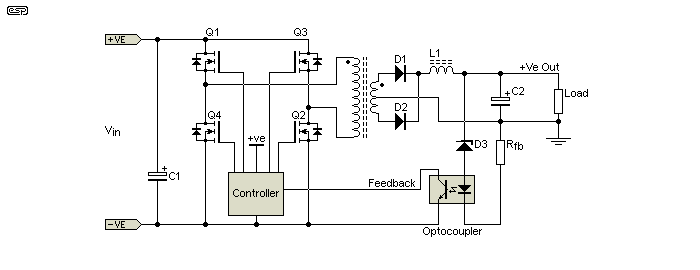
Power is transferred using normal transformer action, when each pair of switches is activated. In the drawing, Q1 and Q2 will always be switched on together, as will Q3 and Q4. Q1 and Q3 are both 'high-side' MOSFETs so must be driven from an IC high-side driver, or they can use transformers. Only two driver transformers are needed because each can have two separate windings for each transistor's gate. If all switches are turned on at the same time, the incoming supply is shorted and instant failure will occur. While it is theoretically possible to build a self-oscillating full-bridge SMPS, it would probably be unwise to do so.
These circuits will generally be used for high power, and the switching devices will be expensive, so it makes sense to include proper control circuits that offer good device protection, soft-start capability and fast, high current driver circuits.
Like the push-pull and half-bridge converters, regulation is only possible if the secondary side uses an inductor.
Due to the complexity of this topology (at least if taken to the extreme), there is little detail in this article. Resonant switching systems offer very low switching losses because all switch commutation is performed (ideally) under zero voltage conditions. The basic circuit is shown below. L1 and C2 form a series resonant circuit, with the transformer being the second 'L' in the name. There are many variations, using series, parallel and series-parallel resonant circuits. Strictly speaking, not all are classified as 'LLC', although they may still use a resonant circuit. Unlike most of the other circuits, voltage regulation is often achieved by changing the frequency instead of using PWM.
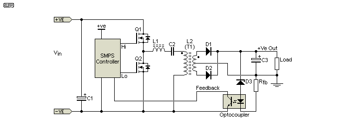
Choosing the resonance frequency and obtaining a stable feedback loop are both difficult, and a brief description cannot do justice to the engineering effort needed to get a stable circuit. One of the primary reasons for adopting this type of converter is to allow higher switching speeds. Switching losses increase with higher speed, but if a resonant circuit can ensure that switching is only performed when there is little or no voltage across the switch, losses become negligible.
The switching frequency may be above, below or at the resonant frequency of the tuned circuit, depending on the desired outcome. Ideally, the current in the tuned circuit will be a sinewave, even though the driving signal is a squarewave. For anyone wanting more information, I suggest Fairchild AN-4151 as a good starting point.
If this topology is used in what may be classified as a 'relaxed' implementation, it's actually fairly easy to make an SMPS. In particular, if it's used in an unregulated converter, many of the benefits can be obtained with little or no added complexity. It's a far better arrangement than a normal half-bridge when driving a capacitive load. The inductor (L1) is often obtained by deliberately winding the transformer in a way that ensures a high leakage inductance. This is normally something that has to be minimised, but it's used in the resonant LLC circuit to eliminate (or reduce the value of) the extra inductor.
Resonant LLC is not restricted to half-bridge converters. It can also be used with full-bridge circuits. The only downside is the requirement for a capacitor (C2) that can handle the high current that's needed for very high power output. Fortunately, this isn't quite as hard as it may seem at first. Polypropylene caps are readily available that are rated for the high current experienced in this type of converter.
Probably the most common combination is the use of a high voltage boost converter, followed by a DC-DC converter. This arrangement is used to provide active power factor correction (PFC), and the incoming rectified AC is not fed to a storage capacitor. The boost converter operates from the pulsating full-wave rectified AC, and adjusts its duty cycle to ensure close to a sinusoidal mains current. The power factor can be as high as 0.97 in a well designed circuit. Unity (1.0) is ideal, and represents a resistive load where voltage and current waveforms are the same, with no phase displacement.
Following the boost converter, the DC-DC converter has a stable and regulated input voltage of around 400-420V DC, and often secondary regulation is not required. There are SMPS designed specifically for LED lighting that use a tertiary switchmode regulator (although it may be combined with the main DC-DC converter). This will usually regulate the voltage to something that's above the LED array's normal operating voltage, but more importantly will regulate the current. Since LEDs have a low impedance, regulating the current provides a more consistent output over time, and ensures that small voltage variations don't cause excessive LED current and subsequent failure due to overheating. Current regulation is shown in the drawing, but not voltage regulation. In most cases, both are used. Voltage regulation is only included to ensure that filter capacitors aren't damaged by over-voltage.
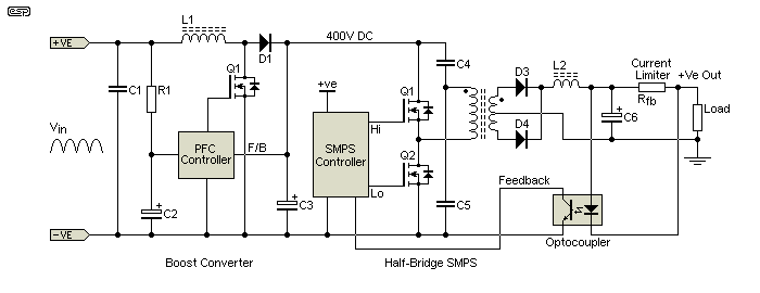
This class of power supply (with active PFC) has become very common in recent years because regulatory bodies worldwide are demanding high power factor from common appliances, luminaires, etc. With the current limiting shown, the above would be used for LED lighting, which requires a constant current output.
Power factor is important because although the consumer only pays for the power consumed for residential premises, a poor power factor means that a higher than normal current flows, and the VA (volt-amp) rating of an uncorrected power supply can be as much as 3-4 times the power. For example, an uncorrected power supply might draw 100W at 230V, but the current may be 1A (230VA) instead of 434mA (100W). This gives a power factor of 0.43 (100W / 230VA).
Despite what you might read elsewhere, phase angle due to inductance or capacitance is not relevant to any switchmode power supply. The input is shown as pulsating 'DC' - it is rectified, but not smoothed. C1 will normally be no more than 470nF and is used to reduce switching noise, provide a low impedance source for L1, and ensure the circuit doesn't oscillate at an unwanted high frequency.
In the above drawing, there is no large capacitor across the output of the bridge rectifier (the input to this circuit). It has simply been moved so it's after the inductor and diode (C3 & C4). This needs to be considered when we look at the next topic, because when power is applied, a high current can flow through L1 and D1 to charge the capacitor before the PFC controller can start to operate normally.
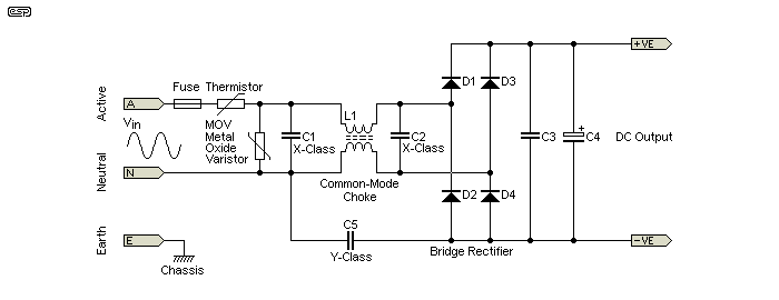
The circuit shown is typical of a great many SMPS. The values of the components is the only difference, with a low power supply needing less filtering (C4) and smaller EMI caps (C1, C2 and C3). The bridge rectifier may be individual diodes or a bridge module, and only standard low speed diodes are needed because the input is 50/ 60Hz mains. The MOV (metal oxide varistor) is included to absorb voltage transients that may damage the circuitry. They aren't generally used on very small supplies, but are common in most medium to high power units.
When any power supply is connected to the mains, there is an initial current 'surge' as capacitors charge, or (in the case of a linear supply) the transformer saturates until steady-state conditions are achieved. Off-line switchmode supplies generally have an EMI filter, bridge rectifier and the main filter cap, and there is little to prevent very high current surges when power is applied. The general arrangement is shown below, and it's common to include an NTC (negative temperature coefficient) thermistor to limit the inrush current, at least to a degree.
Thermistors only work when the current drawn from the supply is steady, and they ideally show a high resistance when cold, with the resistance falling when they get hot. It is expected that the steady state current will be high enough to ensure the thermistor remains at a low resistance, but if it runs hot it is dissipating power. Wasted power in a sealed supply is a problem, because it adds to the overall heat load and raises the temperature of everything inside.
For lighting and many other applications, inrush current can be very limiting. For example, if a 100W lighting fixture normally draws 500mA (a power factor of 0.87), that means that (in theory) 16 luminaires can be operated from a single 8A lighting circuit, although a prudent installer will use fewer - 10 or 12 would be fine. However, if each draws an inrush current of 10A (many are a great deal worse!) the instantaneous current at switch-on can be as high as 120A, and that will cause fuses or circuit breakers to open. Such a high current is also well beyond the ratings for the light switch itself. Something that seemed to be quite alright is anything but, due to inrush current.
It's now becoming common for active inrush limiting to be used. The idea is to ensure that the current drawn at the moment of switch-on is no more than (say) double the operating current. In the above example, that would limit the inrush current to a maximum of around 24A, well within the ratings for fuses and circuit breakers. Active inrush protection adds more parts and cost, but many manufacturers have discovered that not including it causes big problems for installers and customers.
There are many different schemes for inrush limiting, ranging from series resistors with a bypass switch (a relay, MOSFET or TRIAC for AC circuits), NTC thermistors with or without bypass (not recommended as this scheme does not work well and dissipates power needlessly), or purely active systems using one or more MOSFETs. While instantaneous power dissipation may be very high, it lasts for a short time - typically no more than 10 AC mains cycles or around 200ms. During the inrush period, the main switching circuits should operate with a low duty cycle, and it's common to provide a 'soft start' anyway, where the power level is increased gradually rather than providing full power from the instant power is available.
Figure 17 also shows mains filtering components. There's an input capacitor (C1, one (sometimes more) common-mode chokes (L1), each followed by another capacitor (c2). These caps must be X-Class mains rated capacitors, typically designed for 275V AC or more. These filter components reduce conducted emissions - that RF noise that is conducted into the mains distribution circuits via the power supply's mains lead. C5 is (IMO) an abomination, but is very common. Where the supply does not have a protective earth, C5 will be wired to one or both of the AC inputs instead. The purpose of C5 is to reduce EMI, mainly what's called 'radiated emissions' (noise that's transmitted in the same way as broadcast signals).
Buck, boost and other non-isolated circuits can use a direct coupled feedback circuit, because the input and output share a common connection. The feedback circuit is designed to change the switching duty cycle so that as the load increases and the output voltage falls, the duty cycle is increased to provide more power and bring the voltage back to the design value. Feedback networks can be very challenging, because there are several time constants involved and if the feedback is too fast the output can become unstable. If it's too slow, a load change results in an output that takes a relatively long time to correct itself. Feedback network design is complex, and it must result in a circuit that's unconditionally stable. No value of load should cause the voltage to change substantially or become unstable (typically oscillating around the design value but never settling).
Of the isolated designs, flyback converters are relatively easy to regulate, because it's a simple matter to change the duty cycle of the main supply to obtain a regulated output and it's not hard to keep the feedback network stable. Because all secondary windings are close coupled, different voltages can be provided, but with only one having active regulation circuitry. The ratio of all output voltages is determined by the turns ratio - not just between primary and secondary, but also between multiple secondaries. If the voltage for (say) the 5V supply is regulated, then ±12V supplies are set by the turns ratio and will track well over the designed current range. It's common that many supplies require a load on the regulated output before the others will be accurate. The load depends on the circuit used and maximum power output, but may range from 100mA to 5A or so.
With isolated topologies, the feedback loop usually includes an optocoupler - an LED and photo transistor in the same light-proof IC. These are designed to maintain galvanic isolation between input and output circuits, usually to withstand voltages up to around 4.5kV. The LED is driven from a voltage sensor, which can be as simple as a zener diode or as complex as several ICs. In some cases, the LED is driven from a current sensor as well as the voltage sensor. This is done either to provide short circuit protection, or to allow the supply to operate in constant current mode (for driving lighting LEDs for example).
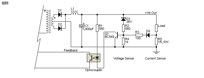
The voltage sensing is done by a zener diode, and if the output voltage exceeds (a little over) 36V the duty cycle will be reduced as the LED in the optocoupler turns on via Q1. The current is regulated to 1A, so with any load from zero up to 1A the voltage will remain at 36V, but a greater load will limit the current and the voltage will fall to ensure that the 1A design current is maintained in the load. The 1 ohm current sensing resistor will cause a voltage drop of 1V at maximum output current, and the resistor dissipates 1W.
A lower resistance can be used, but the voltage drop then needs to be amplified so there's enough to turn on the transistor. Please note that the above is not intended to be a precision feedback circuit, and there will be variations to the design values due to component tolerance. I have shown essential resistors to limit fault or transient current, namely R2 and R3, but again the drawing is only intended as an example, and is not a final circuit.
The term 'magnetics' covers all inductors, chokes and transformers. Cores are almost invariably ferrite, usually a manganese zinc type, and there are many different formulations with differing properties. One of the hard parts of the design is determining the best formulation for the application, deciding on the maximum flux density you wish to use, and deciding how hot it should run. Many ferrites achieve their optimum performance at elevated temperatures. The core material also has to be chosen based on the operating frequency, as a ferrite designed for 25kHz operation may not be able to be used efficiently at 150kHz.
Proper magnetic design will normally ensure that the total losses will be split between copper loss (caused by winding resistance in all windings) and core loss. This is a careful balancing act, and requires knowledge and skills that are well outside the normal knowledge base of most electronics designers. Core loss depends on the switching frequency, flux level and temperature. Many core types show the lowest losses at a temperature of around 80°C or so, and if you ever wondered why SMPS transformers seem to run hotter than expected, this could be one of the reasons.
Switchmode converters of all types operate at high frequencies. The optimum frequency is a trade-off between core size and switching losses. Low frequency operation means that the dynamic switching losses are reduced, but that also means a larger core. At high frequencies, tiny amounts of leakage inductance become a problem, skin effect causes higher than expected copper loss and dynamic switching losses increase. Operating frequencies between 25kHz and 100kHz are common and reasonably trouble-free, and generally still allow the ferrite core to be acceptably small even for surprisingly high power converters.
Where a conventional 50/ 60Hz transformers has many primary turns (perhaps 3-5 turns/ volt for a mid sized transformer), the transformer for an SMPS will use volts per turn. A winding intended for 325V peak-to-peak (~160V RMS) may use 2-3 volts per turn, and may have only 50 turns or so on the primary. During the design phase, the engineer will calculate the maximum flux density based on the peak current, frequency and number of turns. The saturation flux is usually taken to be around 350mT (milli-Tesla), and it is critical to ensure that the core doesn't saturate for most topologies. It's generally wise to keep the flux density far enough below the maximum to ensure that the final design has a safety margin. Typical SMPS designs will keep the flux density to no more than perhaps 200-250mT. Compare this to a conventional mains transformer, where the peak flux density at idle can be as high as 1.4 Tesla.
1T = 10,000 Gauss (older terminology), so 200mT = 2kG (gauss). Higher frequencies mean that flux density must be reduced.
The flux density in a core is determined by the current and the number of turns. Provided the core is not saturated, increasing the number of turns reduces the flux density for a given (constant) input voltage. If the core does saturate, for all intents and purposes it ceases to exist, and the permeability (ability to carry a magnetic field) falls, approaching unity when fully saturated (the permeability of air is 1.0). Strictly speaking, we should refer to 'initial permeability' because with all ferrites it changes with flux density and temperature.
Once the primary turns have been calculated it's fairly straightforward to calculate the turns ratio, and from that the secondary turns can be worked out. As explained earlier, this is an introduction to SMPS, and is not a design guide, and no calculations for turns, flux density or core losses will be covered. There are many dependencies in all calculations, and SMPS design is the subject of many books, countless articles, and (it seems) an infinite number of forum questions and answers.
Although it's not always possible, most design guides suggest that the turns ratio should be as close to 1:1 as possible. While ideal, 1:1 is rarely useful, but it does minimise leakage inductance. Turns ratios up to 7:1 are considered acceptable, and 10:1 can be used if the extra losses aren't likely to cause a problem. Many texts on the subject suggest that turns ratios exceeding 14:1 are not practical. In many cases, the designer has no choice, and the turns ratio is selected based on the required secondary voltage, without fretting about using a high turns ratio. If the design demands a 20:1 turns ratio to get the voltage you need, then that's what has to be used. Ideology and practicality often don't coincide.
When it comes to winding wire, the skin effect is well known (and exploited by snake-oil cable makers). With switchmode power supply transformers it is a real problem, and the most common way to minimise the influence is to use multiple small (insulated) wires in parallel - typically bundled and twisted into a single rope-like strand. This is commonly referred to as Litz wire, and its use reduces skin effect losses because the wire bundle has a comparatively large surface (or 'skin') area.
You don't normally hear much (if anything) of the so-called proximity effect, but it refers to the (often chaotic) disturbance of the current flow in a conductor when that conductor is immersed in an intense magnetic field. This does not appear to be an issue with most SMPS transformers, but in large (low frequency) transformers it can cause localised heating because the current is forced to use far less of the wire's cross section than expected. Use of Litz wire again reduces the proximity effect, and since it's common in high frequency transformers anyway, the effects are already mitigated to a degree. Proximity effect may reduce current carrying ability far more dramatically than does skin effect, and at much lower frequencies.
The proximity effect therefore has the potential to cause localised 'hot spot' thermal problems, that degrade the insulation and cause eventual failure. It is especially problematical when the transformer current is highly distorted, and this is invariably the case when a transformer is used with a rectangular waveform - nearly all SMPS transformers.
It's not at all uncommon for secondaries of high current transformers to be wound using copper foil - a flat sheet that is the full width of the winding space. This provides a large cross sectional area for low resistance, and because it's a flat sheet, the skin effect is minimised. Providing insulation can be challenging with foil windings, as it may occupy far more space than a conventional winding of similar cross sectional area.
The selection of wire gauge is determined by the current and how aggressive the designer is. A good starting point is between 3A and 4A per mm², with higher current density causing greater copper loss and lower density potentially making the winding difficult to fit into the winding window of the core. A one square millimetre wire has a diameter of 1.13mm ( A = π * R² ), and it's often a lot easier to use multiple parallel windings of thinner wire when high current is needed. Where the supply will have only momentary high current demands with a somewhat lower average demand, it's usually possible to use a higher peak current density than 4A/ mm², provided the average is somewhat lower. This requires experience and careful design.
Vout = D × Ns / Np × Vin
D is duty cycle, Ns is secondary turns and Np is primary turns
Output voltage of PWM squarewave converters can be estimated by the formula shown above, but it doesn't work for all converter types and should be considered a rough guide at best. However, it's a useful start and can be used to get a general idea of what the converter will do. It won't work with flyback converters, because they operate by utilising the back-EMF from the transformer to generate the secondary voltage. The duty cycle or 'on' time of the switch is changed to store more or less energy as needed. Remember that a flyback converter transfers no power when the switch closes - only when it opens.
In most of the circuits shown above, there is a controller shown as a 'black box'. There are many different ICs designed for SMPS, and the vast majority use a simple resistive start-up circuit. Some need an auxiliary winding (commonly known as a 'bias' winding) on the main transformer or inductor. This is used to provide the normal operating voltage and current for the IC, via a very simple power supply - often nothing more than a couple of extra turns on the transformer and a single extra diode. It's unusual for any controller IC to use only the resistive start-up supply for normal use, because relatively high peak current is needed to drive the MOSFET gate(s) and drawing that through a resistor from the 325V DC supply causes excessive power dissipation.
The general idea is shown below, and the start-up supply only needs to provide enough energy for two or three switching cycles. After that, the auxiliary supply takes over and provides the power needed for normal operation. It's not uncommon to include a voltage divider (R2 & R3 below) to sense the main supply voltage, so the power supply will shut down if the input voltage is too high or too low. This protects the SMPS from excessive current due to a low input voltage, or damage if the voltage is too high.
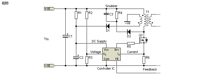
In the above, the start-up current is provided by R1, and once the SMPS is operating D1 provides the supply voltage via the tertiary winding on transformer T1. R1 is selected to be able to supply enough current for the controller to start, but cannot provide enough for normal operation. This is done to minimise the resistor's dissipation. The incoming voltage is sensed by the controller after the voltage divider formed by R2 and R3. This enables the controller to turn the supply off if the voltage is too low to allow normal operation, or is too high, placing the switching MOSFET at risk.
R6 is used to sense the current in the switching MOSFET (Q1). Current sensing ensures that the supply can protect itself in case of a shorted output, and it usually monitors each switching cycle so that any fault that causes the MOSFET current to exceed the design maximum will cause the supply to shut down immediately. Shut-down may be 'latched', meaning that the supply will require a power cycle (hard reboot), or it may retry at preset intervals until the fault is cleared. The latter is more common.
The snubber circuit (C3, R4 & D2) is designed to limit the amplitude of voltage spikes when Q1 turns off, and is a lossy circuit. Any power consumed by the snubber is wasted, so it's important to optimise the transformer design to ensure that the wasted power is as low as possible. There are many variations for snubber circuits, and sometimes they can even be dispensed with. This is circuit dependent, and 'snubberless' designs are not common. There's even a few very clever (and patented) methods of using the snubber to provide auxiliary power.
Many SMPS are designed for low power applications, often where they will enter a standby mode where power consumption has to be as low as possible. Many countries have requirements that standby or no load operation should result in the supply drawing no more than 0.5W and sometimes less. One way to achieve this is to use what's called 'skip-cycle' mode, where the supply maintains its output voltage by operating the main switching device at a very low repetition rate. Rather than running at 50kHz or more all the time, a couple of cycles at 'normal' speed may be enough to keep the output voltage above a preset minimum for somewhere between a few milliseconds to perhaps a second or more. During the off state, very little power is drawn, thus keeping the average consumption well below the maximum allowed.
Not to be confused with inrush current limiting, most dedicated SMPS controllers feature a 'soft-start' feature, where they start operation after power-on with a very low duty cycle. The duty cycle is increase steadily until normal operation is reached. This ensures that magnetics and other circuitry have time to stabilise before the supply reaches full power, and also helps to minimise inrush current because everything doesn't happen at once. First the inrush limiters bring the voltage up to normal, then the soft start circuits increase power output. While the description takes some time to read, the whole process may only take about 200ms from the moment that power is applied, and is usually barely noticeable by the user.
One of the main goals of any SMPS is to ensure the highest possible efficiency. One of the things that always places a limit is the humble rectifier diode, as there is a voltage across the PN junction that is dependent on the basic junction characteristics. A normal high speed diode will have a forward voltage of 0.65V at low current, but there is an inevitable resistive component as well. That means that at rated current, the forward voltage might be 1V or more. If the forward current is 10A, dissipation is 10W. Two diodes used as the output rectifier for a 10A supply will each pass 10A for around 50% of the time, so the loss just due to the diodes is 10W continuous.
Schottky diodes are better, but are only suitable for low voltages, typically limited to around 50V reverse breakdown (although there are exceptions - up to 250V). This is due to the internal construction of these diodes. The forward conduction voltage can be as low as 150mV, but the resistive component still exists. A diode such as the MBRAF440 is rated for 40V, 4A, and has a forward voltage of 0.485V at 4A and 25°C junction temperature. Dissipation is therefore less than 2W for each diode, but for 10A the best we can hope for is around 5W total dissipation.
You may have noticed that none of the example circuits use a bridge rectifier at the transformer output. Even Schottky diodes will have excessive losses when used for low-voltage high-current applications, and a bridge simply doubles the loss. It's easier (and cheaper) to use a centre-tapped transformer. This is in marked contrast to conventional mains frequency transformers, where the centre tapped arrangement is inferior due to poor winding utilisation and much greater losses due to many turns of wire. Also, it's uncommon to try to get a high current 3.3V or 5V DC output (for example) directly from a normal mains tranny, but this is a very common use for switchmode supplies.
Synchronous rectifiers generally use MOSFETs. All MOSFETs have an internal diode, but that's effectively shorted out when the MOSFET is turned on. By synchronising the MOSFET drive signal, it can act as a very low-loss rectifier. The internal diode is fairly ordinary, but when the MOSFET is turned on there is only the RDS(on) figure (on resistance between drain and source) to contend with. For example, an IRF540N has an on resistance of 44mΩ, so at 10A the voltage drop will be 0.44V - not zero, but lower than any diode. This limits the dissipation to 4.4W, and two in parallel reduces that further to 2.2W - better than any conventional or Schottky diode can ever manage. There are many other MOSFETs with even lower on resistance, for example IRFZ44E, IRFZ46N with 23mΩ and 20mΩ respectively. The On-Semi BXL4004 is even lower - 3.9mΩ.
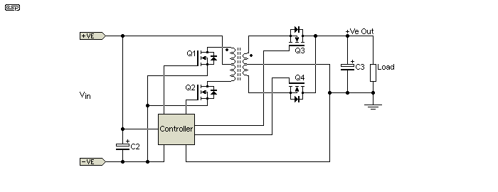
Of course there is a down side. The MOSFET(s) need a control signal, and it has to be carefully managed to ensure that the MOSFET is never turned on when its internal body diode would not be conducting. This adds parts to the design, but they all operate at low power so there's very little efficiency penalty. The synchronous rectifier MOSFETs are Q3 and Q4, and each is turned on when the diode would normally be conducting (i.e. when the voltage across the MOSFET is reversed). The whole process is rather non-intuitive, but it works and is recommended in many papers on the subject. It's not obvious, but MOSFETs conduct with either polarity between drain and source, and that's how they can be used in this application. With optimum devices, their voltage drop is far less than any diode, and rectifier losses can be (almost) eliminated. Instead of losing a volt or more across diodes, the loss can be limited to well under 100mV with the right MOSFETs.
In the same way that switching devices used with push-pull, half and full-bridge converters must allow a dead band, the same applies with synchronous rectifiers. The above drawing is highly simplified and is not intended to refer to any specific controller. In some cases, the rectifier MOSFET gates may be driven by small pulse transformers, or can be driven directly by the transformer output for some designs (see Figure 24). Synchronous rectifiers are not only used as shown above - they can also be added forward converter SMPS, or to buck, boost, buck-boost, SEPIC or Cuk non-isolated DC-DC converters. It should also be possible to use the scheme with a flyback SMPS, but it's probable that there would be little to gain.
With any switchmode supply, losses are minimised by ensuring that the MOSFETs or IGBTs are switched on and off as quickly as possible. The same applies to BJTs of course, but they aren't used in many SMPS any more because they are too slow - especially to turn off. Both MOSFETs and IGBTs use an insulated gate, and there is capacitance between the gate and the remainder of the device. This capacitance can be quite large (several hundred picofarads or more), and the gate drive must be capable of charging and discharging the capacitance in the shortest possible time.
Many commercial gate driver ICs exist that can deliver 2A or more for a short time, with the sole purpose of ensuring fast charge and discharge of the gate and any stray capacitance. One is shown in the next section, but there are hundreds of different types, including specialised 'high side' drivers. These are designed to interface with normal 12V signals, but provide a method of driving MOSFET gates that may be at 400V or more above the controller's operating voltages. There are also high-side drivers that just allow the use of an N-Channel MOSFET in circuits such as those shown in Figures 5 and 7. Rather than allowing a big voltage differential, these provide enough voltage to turn on the MOSFET, above the supply rail. For example, the supply voltage might be 12V, and the high-side driver supplies a gate voltage of 24V by one means or another. There are countless different designs using a wide variety of techniques.
One common system is to use a 'charge pump', a circuit that acts as a voltage doubler (often with the required capacitor integrated within the IC). This allows the gate drive voltage to exceed the supply voltage, so an N-Channel MOSFET can be used where one would otherwise have to use a P-Channel device. The availability of the P-Channel types is nowhere near as great as for N-Channel, and N-Channel devices typically have around one third the on-resistance of a P-Channel part of the same size and cost.
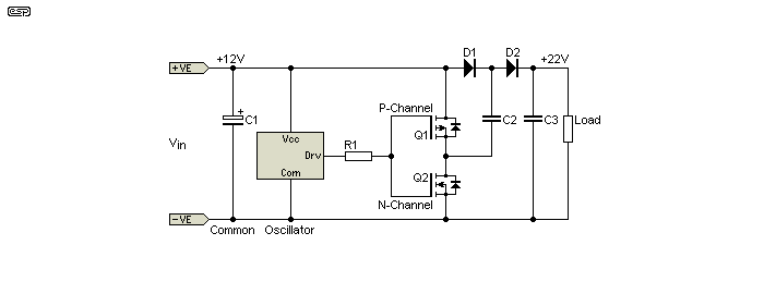
A conceptual circuit for a charge pump is shown above. When Q2 turns on, the end of C2 is connected to the common bus, and it charges to the supply voltage via D1 (less a diode voltage drop of course). Now Q2 turns off and Q1 turns on. C2 is charged to a bit under 12V, and D2 conducts and passes the charge to C3 which will be charged up to around 22V. This really is only a conceptual circuit - the MOSFET gate drive needs to incorporate a dead time to prevent shoot-through current. There are many ICs that have all the circuitry needed, and in some cases that even includes C2, and there is nothing else needed (the MAX1614 is a case in point). When more current is needed (for a proper SMPS for example), the IC is likely only to contain the oscillator and MOSFETs, and the diodes, pump capacitor (C2) and output cap will be external.
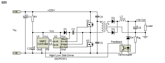
Another common system is called bootstrapping - essentially it works in exactly the same way as described for the charge pump. This arrangement would be used to turn on the MOSFET(s) in a half or full-bridge SMPS as shown above. In both these cases, N-Channel MOSFET(s) that connect to the incoming supply need a gate voltage that's around 12V more than the supply itself. When Q2 turns on, C3 is charged to Vcc (e.g. 12V), and when Q1 turns on (Q2 is now off) the high-side driver inside U2 is powered by the charge stored in C3. The voltage at 'Vboot' will be around 337V, 12V more than the voltage at the source terminal when the MOSFET Q1 is on, and the gate will be driven to the full bootstrapped voltage.
How much drive current is needed for a typical MOSFET? An IRF540N was simulated using a 12V gate drive with several rise and fall times, and the peak current was the same for rise and fall. A 100ns risetime demanded a peak current of 700mA, rising to 1A with 50ns and 1.2A at 25ns. The IRF540N is claimed to have a gate capacitance of almost 2nF, but there's also capacitance between the drain and gate (the 'Miller' capacitance). MOSFETs are usually rated for the total gate charge, measured in Coulombs (symbol C) - the charge transferred by a constant current of 1A flowing for 1 second. The total gate charge for the IRF540N is 71nC. This total gate charge must be overcome every time the MOSFET is turned on or off, and the current needed depends on the switching speed - higher speed means more current.
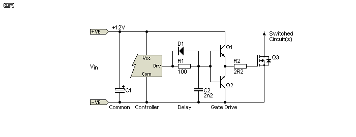
The above drawing shows a common gate drive technique, using a pair of bipolar transistors. This arrangement can deliver more than enough gate current with the right transistors, and the delay circuit introduces some dead time. When the output from the controller goes high, C2 has to charge via R1, introducing a delay (it only needs to be around 0.1µs ... 100ns). When the controller's output goes low again, C2 is discharged via D1, minimising the delay. It's not really a delay, just a simple filter, and the turn-on time of the MOSFET is increased slightly. The two transistors provide significant current gain, minimising the load on the controller.
With the values shown, the MOSFET turn-on is delayed by about 130ns, and gate voltage is removed almost immediately. The turn-off time depends on the MOSFET. This circuit can be seen in many SMPS, because it's simple and cheap to implement. However, if a suitable controller IC is used it shouldn't be needed, because there will be provision for dead time and a high current MOSFET gate drive within the IC itself. Most dedicated ICs use MOSFET drive (similar to the complementary MOSFETs shown in Figure 20).
There are many gate drivers available, including simple low-side types, dedicated high-side versions, and others that combine the two. Some have limitations as to the peak current they can source or sink, and require low gate-charge MOSFETs. Some Class-D amplifier ICs require the use of special MOSFETs for exactly this reason. It's worth noting that a Class-D amplifier is simply a specialised SMPS that has been designed specifically to handle audio frequencies rather than provide a DC voltage.
A Class-D amplifier can easily be 'tricked' into thinking it's supposed to be a voltage regulator, but it won't provide optimum performance in that role. Overall though, the primary difference between a Class-D amp and an SMPS is that the Class-D amp can both sink and source current, and provide an output that can be positive or negative. SMPS (like most power supplies) are designed to source current of one polarity only, and they can't absorb current that may be provided by the source. This a topic unto itself.
A complete SMPS using many of the principles explained above is adapted from a TI user's guide for an evaluation PCB. The circuit is a 48V to 3.3V 10A forward converter, and uses instantaneous peak current detection for the switching MOSFET, and a self-powered synchronous rectifier. I looked at a great many different circuits, but this one seems to show most of the topics covered above. The main controller part number in the original TI schematic is wrong which isn't helpful! Note that a separate 12V supply is required for the controller IC.
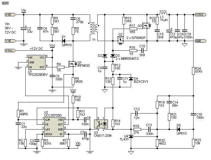
The main switching MOSFET is Q1, and it's driven by U1 - a dedicated gate driver as discussed above. The TPS2829DBV is now obsolete, but it provides 2A gate drive and 25ns rise and fall times. The main controller (UCC35705D) provides the PWM switching waveform, instantaneous MOSFET current monitoring and full regulation via the opto-coupler.
Voltage is monitored by U4, a TL431. This is a programmable shunt regulator, and will turn on the LED in the opto-coupler to just that level needed to stabilise the output voltage at 3.3 volts. The components around the TL431 are to ensure feedback loop stability. SMPS feedback is not straightforward, and it's always necessary to provide networks to obtain the time constants needed to keep the loop stable. Direct feedback without compensation networks would cause the entire supply to be unstable, typically with an output that oscillates around the desired value.
The feedback loop must remain stable as loads are connected and disconnected, and must also remain stable with any load from zero to the maximum allowed. It's very common for SMPS to have complex and convoluted compensation networks, and the circuit shown is a perfect example. C16, D5 and R23 provide a soft-start that's intended to prevent output voltage overshoot at start-up. Overshoot at start-up is normal with any choke input filter - in this case L1 and C17, C18, C19, and the time constants involved make feedback loop stabilisation all the more difficult. Three different value capacitors are used to ensure low impedance over a wide frequency range. Switchmode supplies need bypassing that's effective up to at least 10MHz because of the very fast switching time.
The MOSFETs (Q2 and Q3) used as rectifiers are designed specifically for this application, and are driven directly from the transformer secondary. No additional circuitry is used, other than snubber circuits in parallel with each MOSFET. The overall efficiency is claimed to be 85%, and that could not possibly be achieved without the MOSFET rectifiers.
At present, this is the only article covering switchmode supplies in any detail, although there is some more info in the Lamps & Energy section of the ESP site. Depending on demand and my workload, I may add another article with some experimental circuits that readers can play with to become better acquainted with SMPS techniques.
There can be no doubt that switchmode supplies will be used in more and more products over time. There are now very few linear supplies used in common household products, and items such as TV sets, set-top boxes, DVD (and other) players, home theatre receivers, microwave ovens, induction cooktops and air conditioners all use switchmode supplies. Linear supplies are still the most common for DIY, simply because SMPS are unsuited for inexperienced constructors, and are a technology that is really only economical when made in large numbers. For hobbyists, the difficulties of getting the controllers, MOSFETs and (most difficult of all) the magnetics mean that a home-build is not really feasible except for a few diehard experimenters. Most of the parts needed are SMD, and there is zero tolerance for errors. Making an SMPS without a PCB is extremely difficult, especially if SMD parts are used.
A home built linear supply will just blow the fuse if a mistake is made, or possibly there will be no output. With most SMPS designs, many opportunities for errors exist, most of which will result in instantaneous destruction of switching MOSFETs and other parts. They are completely unforgiving of assembly errors, and since many include under-voltage protection, you can't gradually increase the voltage with a Variac to make sure that everything is ok. What happens instead is nothing ... until the voltage exceeds the preset under-voltage threshold. The supply then attempts to run - if there's an error all the protection circuitry in the world is unlikely to help.
It's also important to understand that most of the 'interesting' circuitry operates with a direct connection to the mains, and poking around and trying to take measurements of an operating (or misbehaving) supply is extremely dangerous. You can use an isolation transformer of course, but that only makes the situation a little bit better - there will still be high voltages (up to 420V DC) with very high instantaneous current capability. If you happen to connect yourself across that sort of voltage, you may not survive.
This isn't to say that home building of SMPS isn't possible - it can certainly be done. Naturally enough, most DIY builders won't be able to test for EMI, and it may transpire that their pride and joy wipes out radio or TV reception for themselves and many neighbours as well. If that happens, there aren't many choices other than to try putting it into a metal enclosure, and if that doesn't work it becomes a door-stop.
Design is not trivial at any level, despite web sites that can create a design to your specifications in seconds! Like all electronics it's an interesting endeavour that will give great satisfaction when the project works. The converse it also true, and if it doesn't work, it may not even be possible to fix it. Compare this to a linear supply, where almost everything operates at relatively safe voltage levels, and even gross errors will just cause a fuse to blow (or a capacitor to explode!). Twenty years later, it will still be easy to fix it if something goes wrong. PCBs are not necessary for simple supplies, and everything can be replaced and/ or a substitute part found.
The half-life of many SMPS parts is very short, and you may find that the controller you used is no longer available in as little as a couple of years after you built the supply. Other parts may also become obsolete very quickly, and since a PCB is essential it may not be possible to use a substitute part because it won't fit the PCB. Commercial products have similar issues, and it's uncommon for suppliers to repair SMD PCBs - they are replaced, and when the required board is no longer available the product can't be fixed at all. This is very common now, and cannot be expected to improve. A perfect example is the circuit shown in Figure 20 - one of the main ICs that the circuit relies upon is now obsolete (although there does appear to be a compatible replacement).
 Main Index
 Articles Index
| Copyright Notice. This material, including but not limited to all text and diagrams, is the intellectual property of Rod Elliott, and is Copyright © 2015. Reproduction or re-publication by any means whatsoever, whether electronic, mechanical or electro-mechanical, is strictly prohibited under International Copyright laws. The author (Rod Elliott) grants the reader the right to use this information for personal use only, and further allows that one (1) copy may be made for reference. Commercial use in whole or in part is prohibited without express written authorisation from Rod Elliott. |