

|
| Elliott Sound Products | Flyback SMPS |
 Main Index
 Articles Index
After (or before) reading this, I recommend that you also read Dangerous Or Safe? - Plug-Packs (aka 'Wall Warts') Examined, which covers the hazards in some detail. It also explains why buying from sellers that distribute products directly from Asian manufacturers is a really bad idea. If you build your own, it's likely to be just as dangerous as many of the examples shown in that article, and quite possibly even more so.
Once you start looking at the details, the idea of DIY becomes less attractive. One of the biggest hurdles is the transformer. There is absolutely no doubt that you can wind the transformer, as the number of turns is generally low. You typically only need up to around 150 turns for the primary, and even fewer turns for the bias and secondary windings.
The bias (aka auxiliary) winding supplies the switchmode IC with power (there's a startup process that provides just enough to get the switching circuit to function). The secondary winding provides isolated DC to the device being powered, after rectification and filtering. The secondary winding must be isolated from the mains to a very high standard. Should the insulation fail, 'bad things' will happen.
WARNING : The following circuits are connected the mains and must never be tested without extreme care. An isolation transformer is essential if you intend to take measurements while the supply is operating. All circuitry must be considered to operate at the full mains potential, and must be treated accordingly. The DC output should be earthed via the mains safety earth to provide an additional safety 'barrier'. Do not work on the power supply while power is applied, as death or serious injury may result.
Under no circumstances should anyone who is not experienced with mains voltages attempt construction or examination of switchmode power supply, as even a small error can be very dangerous. Great care is needed - always! By continuing, you accept all risk and hold ESP harmless for any death or injury suffered.
Just as there is no doubt that anyone can wind the transformer, there's no doubt that very few people will have the equipment needed to test it for electrical safety. When you buy a small SMPS, provided it has approvals for your country, it will have passed all necessary tests for electrical safety and EMC (electromagnetic compliance/ compatibility). These tests require equipment that very few hobbyists will possess.
If you make an error with the insulation of the transformer, such as too little creepage or clearance distance between windings or the wrong type of insulation material, you can easily have an electrical breakdown that places the user at risk of electric shock or electrocution. As the person who built the circuit, you will be directly responsible for any injury or death, and you may be prosecuted (assuming that the injured person is not you).
There are countless 'projects' on the Net telling you how to build your own off-line (mains powered) switchmode power supply (SMPS/ PSU). Many of these are rated for 1A or so, with voltages ranging from 3.3V to 12V. As a hobbyist and 'creator', the idea is (at least initially) appealing, as much for me as anyone else. The simplest SMPS is the flyback type, and many ICs are available that are designed specifically for this application.

Beware of YouTube (and other) videos that show you how to build a flyback supply. All that I saw neglect nearly everything that's important. While it's certainly possible to build your own SMPS, be aware that it's not advisable. Build one for testing and experimentation by all means, but using it in place of a commercial approved SMPS is ill-advised.
Without adequate testing (with equipment you almost certainly don't have), you have no idea if your insulation is acceptable, and nor do you know that it will remain acceptable for the expected life of the product. Most on-line circuits never cover this with sufficient clarity to ensure that the builder gets it right, so you may have constructed a 'time-bomb' that fails catastrophically or lethally several years after it's been built.
Most small SMPS don't use vacuum impregnation for the transformer, but that's one way to ensure that it remains safe for years to come - assuming it was safe beforehand. Few hobbyists have the equipment for this procedure, so the constructor will never know for certain that the transformer can never short between live (hazardous voltage) to the secondary.
In general, you need a transformer with a rated dielectric strength of at least 2.5kV RMS (preferably 3kV RMS), as this provides the safety barrier between mains and the end user. Despite a fairly well-equipped workshop, I can't test anything at that voltage, as I don't have anything that can provide it with any degree of safety. If you buy a suitable transformer, the datasheet will include the isolation specifications.
Then there's the cost. You need a PCB, the switching IC, a transformer (either ready-made or DIY), capacitors, bridge rectifier, at least one high-speed diode, an opto-isolator and zener diode (or variable voltage reference) and input/ output terminals. The IC is the easiest, but the device you use then determines the specifications for the transformer, and finding compatible parts isn't always easy. You can buy SMPS transformers that will (hopefully) be safe, but you still need to know exactly what to look for. There are several transformers that look ideal, but they don't have a high enough isolation voltage to be useful. Not all flyback SMPS are used with a mains input, and some are designed (as DC-DC converters) to provide isolation between different parts of internal circuitry.
You can buy a small (12V, 1A) SMPS as a plug-pack for around AU$18 or so (some as low as AU$13 in bulk), and if purchased from a reputable supplier it will be rated as Class-II (double insulated) and have full approvals for your country. It will have been tested for electrical safety and EMC, so you get something that contains all the required safety and filtering parts that are essential for safe (and legal) operation. If you need an internal PSU in a chassis, it's an easy matter to split the case and remove the PCB, which can then be installed in a small ABS plastic 'utility' box and installed.
If you decide to build your own, you'll still spend about the same (probably more), but you won't know if it will pass any of the tests that are usually mandatory. What you do get is experience with the design and construction of the PSU, along with the fun of doing so. At the end of the exercise, you (hopefully) get a power supply that will work, but it's one that you probably shouldn't actually use. If it's installed inside Class-I equipment (protected by a mains earth/ ground 3-core mains cable) it might be 'safe', but if your insulation fails expect a spectacular fuse failure as a result.
Naturally, you can buy the required test equipment to test for electrical safety. The cheapest I've seen is 'only' AU$1,500, but most are considerably more expensive. Testing for EMC will set you back at least AU$10k (but probably a great deal more).
A 'home-made' PSU can never be rated for Class-II (double-insulated), because it's virtually impossible to run the necessary safety tests without certified test equipment designed for the job. Not one 'DIY' SMPS article I saw includes this important point, and I shudder to think how many home-made power supplies are out there waiting to kill someone.
The flyback topology is popular, because it's the lowest cost option for low to medium power. Up to around 150W is possible, but other circuits perform much better at higher power levels. One thing that the reader may (or may not) have noticed is the polarity indicators on the transformer windings. The dot traditionally indicates the start of the winding, and flyback transformers always have the primary and secondary (or secondaries) operating with inverted windings. The basic principle has existed for as long as 'electronics' as we know it. It's also the underlying principle of the spark coil in a (petrol) car engine.
Considerations for use as a power supply are many. Cost is almost always among them, but technical issues are regulation, transient performance, ripple and filtering, EMI generation, efficiency at specific load points and across a load range. One also needs to consider size, weight, BoM complexity, stability, temperature, and performance despite component tolerances. Other factors include isolated vs. non-isolated designs, which are defined by the application.
The flyback principle is the same as that for a relay or other electromagnetic coil. Many people will have experienced the high-voltage 'spike' generated when a relay coil is disconnected. The peak voltage can rise to hundreds of volts and is quite capable of destroying the switching transistor. The standard fix is a diode in parallel with the coil. A flyback circuit just adds another winding, and delivers the flyback pulse current to the load, rather than 'wasting' it in a diode. For mains use, Flyback circuits are (almost) invariably galvanically isolated, having no conducting material (wire or other conductor) between the input (mains) and the output (user accessible voltage). Instead, current is transferred magnetically, and feedback usually involves an optoisolator.
When the power switch operates, current flows through the transformer primary via the switching MOSFET. This is either internal to the IC for low power, or external for anything above around 12W or so. The origin of the flyback circuit (as we know) it dates from the 1940s, with the introduction of television. A flyback circuit was used to generate the CRT horizontal sweep (when the switch was 'on'), the 'flyback' or retrace sweep (switch off), and also to generate the EHT voltages for electron-beam acceleration and focus. However, the principles were known well before the introduction of TV.
A flyback transformer is not a transformer in the traditional sense. It's really two or more coupled inductors. With a 'true' transformer, current flows in the primary and secondary at the same time, with the two being in-phase (assuming proper connection). In a flyback transformer, no current flows in the secondary while current builds up in the primary. When the switching device turns 'off', current is induced into the secondary winding. This is not 'transformer action' in the accepted sense.
Most flyback converters are operated in discontinuous conduction mode (DCM), as this minimises the size of the magnetic component (the transformer/ coupled inductors) and makes the job of the secondary rectifier a little easier, as there is no current flow when it turns off. In the explanations that follow, DCM is assumed in all cases. The alternative is CCM (continuous conduction mode) where the DC component in the primary never falls to zero. These are not covered here, but they may be used to minimise RF interference or to minimise the size of filter components.
The two states for the switch are tON ('on' time) and tOFF ('off' time). When the switch closes, current builds in the transformer's primary, storing energy in the magnetic field. The switch 'on' time must be long enough to store the energy needed, but short enough to ensure that the core doesn't saturate, as this will cause high current and switching MOSFET failure. Many ICs have current monitoring to limit the peak current to a safe value. For example, the VIPer22A limits the peak primary current to 700mA.
The following circuit was used for simulations. CX2 is an X-Class (275V RMS) mains capacitor, and it works in combination with LEMI to suppress electromagnetic (RF) interference. All of the examples that are shown further below use the same principle. There are very few apparent variations with flyback converters, regardless of the IC used or the power level. The control mode is PWM, where the 'on' time of the switch is varied. At low output power the switch will only be 'on' for a very short time, and the 'on' time is increased as the load current increases to maintain the desired output voltage. While the example assumes a fixed frequency, many flyback control ICs use variable/ modulated switching frequencies.

In its simplest form, a flyback supply consists of a pulse generator, a switch and a transformer. Because we want DC at the output, there's a rectifier diode and a filter/ storage capacitor on the secondary of the transformer. Current flows in the primary circuit when the switch (MOSFET) turns 'on', and current flows in the secondary when the MOSFET turns 'off'. The pulse generator will run at a minimum of 25kHz, with around 60kHz or more being more common. The peak primary current is determined by the 'on' time and the inductance of the transformer primary.
The transformer's magnetic core is usually ferrite, and it must include an air-gap. Inclusion of the air-gap means that more primary turns are needed for a given inductance, due to reduced core permeability. Technically, the stored energy that's released to the secondary is not contained in the core, but the gap. To avoid introducing a large amount of leakage inductance, the winding must fully enclose the gap (for 'E' type cores, the gap is on the centre leg).
Early versions of flyback converters used bipolar junction transistors (BJTs) or even valves (vacuum tubes) for early TV sets, but these were too slow for efficient operation at high frequencies. Switching losses are generally significantly higher with a BJT. MOSFETs are almost universally used as the switch of choice.
The secondary diode's reverse voltage rating must be higher than you think. The diode typically needs a voltage rating of at least 5 times the output voltage under load, but it can be a great deal more with no load. Even for a 5V output you typically need a minimum of 36V (a 40V diode is just sufficient). I measured a small 5V SMPS (similar to that shown in Fig 7.1), and with no load the diode's reverse voltage was 42V peak. Many designs use Schottky diodes because they have a lower forward voltage and hence a lower power loss, but others use 'normal' high-speed diodes. You cannot use a standard diode such as 1N4004/ 1N5404 etc., as their turn-off is too slow and they will overheat and fail. The RC snubber across the output diode is usually omitted, but may be required to suppress RF interference.
The RCD snubber circuit shown is intended to minimise the voltage spike generated by the transformer's leakage inductance. This is covered in detail in the Transformers, Part 2 article (the link takes you directly to the section that covers leakage inductance). Leakage inductance causes damped ringing when the switch turns off, as seen in the waveforms shown below. Leakage inductance is shown as Lleak, and it's a lossy (Rdamp)) parasitic inductance caused by imperfect containment of the magnetic field within the core. The value shown is an example, but note that Lleak is not a separate component - it's part of the transformer and unavoidable in 'real life'. Ideally, leakage inductance will be as low as possible.
When the switch turns 'off', a high voltage would normally appear across the primary, but instead the energy is transferred to the secondary, and via D1 to the filter cap and load. In 'real' (as opposed to 'imaginary') SMPS, the pulse generator is controlled via feedback, so the pulse-width (MOSFET 'on' time) is just enough to supply the load current. In many cases, the lowest possible pulse width will still be too much with very low (or no) load current, so the controller will inhibit pulses for several cycles. This is commonly known as 'skip-cycle' operation. The output voltage ripple is usually higher than normal in this mode.
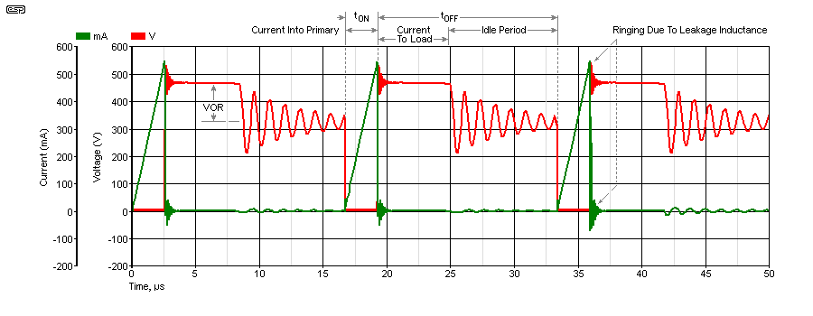
Figure 1.2 shows the primary waveforms with annotations. The red trace is voltage, and the incoming DC is nominally 325V (rectified and smoothed 230V RMS). When the MOSFET turns on, the voltage falls to zero and current (green trace) starts to increase. The 'on' time is about 2.43µs, during which time the current rises to about 545mA. When the switch turns off, the voltage across the primary winding increases to 472V as the magnetic field collapses. The stored energy is dissipated via the secondary diode, as it charges the output filter capacitor and supplies the load current. Once the primary's stored energy is depleted the circuit is 'idle', and it will 'ring' at a frequency determined by the primary inductance and stray capacitance. A scope capture of the voltage from a real flyback SMPS is almost identical to that simulated (see below).
The parameter shown as 'VOR' is sometimes referred to as 'reflected voltage', and it's the output voltage across the secondary, reflected back through the transformer and multiplied by the turns ratio. It's not my intention to go into detail about transformer design, but suffice to say that this is not a matter of guesswork, but is a highly refined process. IC manufacturers often provide dedicated software to assist with the design, or sometimes spreadsheets. The transformer is the most critical part of the design, and it's essential to get it right to enable maximum efficiency and low no-load losses.
Calculating the peak primary current is not easy, but it's a function of time, inductance, applied voltage and circuit resistance. Most transformer design procedures will cover this in detail. I don't propose to go into this here, because as already noted I don't consider a DIY flyback SMPS to be a viable proposition. However, I will offer the following ...
ΔI/Δt = V / L
Where ΔI/Δt (aka dI/dt) is change of current over time (amps & seconds)
V is voltage
L is inductance
If this is calculated for 325V and 1.5mH, the answer is a rather large 217kA/s (yes, that's kilo-amps). Since we have an 'on' time of 2.6µs, we simply divide by 1 million (106) to get current per microsecond, and multiply by 2.43 (µs). The final answer is 548mA peak, which agrees quite well with the simulation (the error is less than 1%). Because the resistance is so low (5Ω) it can be ignored for a current of less than ~500mA, but you may need to adjust the voltage to compensate if it's much higher. Remember that in normal use, the SMPS will be powered from the mains, which can vary by up to ±10% (207 to 253V RMS for nominal 230V mains).
The peak current cannot be increased beyond that which causes the maximum recommended flux density for the core being used, as it will saturate. Once a transformer core is fully saturated, it effectively ceases to exist, and the current is limited only by the series resistance. Because there is a net DC in the primary waveform, transformers used for flyback SMPS always have an air-gap. This has to be calculated too, and it reduces the inductance (compared to the same number of turns with no air-gap). In most flyback designs, the duty-cycle (ratio of 'on' to 'off' time) is almost always less than 50%. The flux density in a flyback transformer increases with higher output current (and therefore a longer on-time). This is the opposite of a linear (mains frequency) transformer, where the flux density is reduced as output current increases. They are different in nearly all respects, and cannot be compared!
The highest flux density will be at maximum output load and minimum input voltage, because the switch 'on' time is at its maximum. If you look at the specifications for wide-range (small) switchmode supplies, efficiency is generally higher with 230V AC input than with 120V input. The output voltage (without feedback) is directly proportional to the input voltage for the same on-off ratio. The feedback circuit changes the ratio in 'real time' to ensure the output voltage is stable.
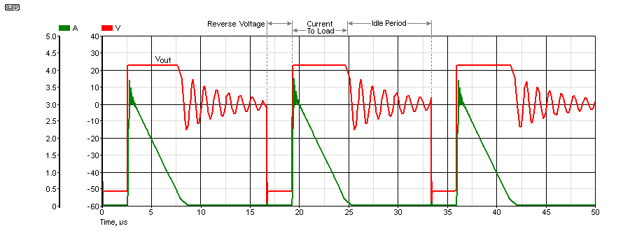
The secondary voltage and current are shown in Fig 1.3, and you can see that the peak reverse voltage is fairly high. For the simulated circuit shown in Fig 1.1, the DC output voltage is about 22V, and the diode's peak inverse voltage is over 90V (including the ringing 'spike'), both with a 47Ω load resistor (468mA DC output). The peak diode current is 3.5A, over seven times the average DC. It's easy to be caught out by the behaviour of the secondary circuit, because most initial assumptions will be wrong! Unless you've taken serious measurements you'll be completely unaware of the reality. I tested a 5V 1A SMPS (after repair because the output rectifier had failed), and found that the diode was subjected to a reverse voltage of 42V with 230V mains. That's more than eight times the output voltage.
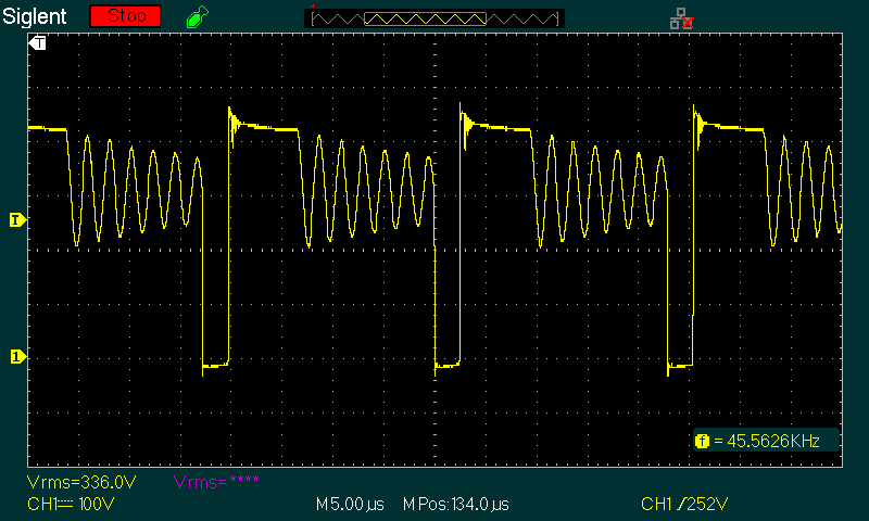
As for waveforms, the final one is a scope capture from a 24V, 4A flyback SMPS, operating with a 600mA load. The peak amplitude can be seen to be about 450V, and the MOSFET 'on' time is 2.5µs. Power is delivered to the load for 6.5µs, after which the transformer 'rings' for 6 cycles (no appreciable power is consumed, as evidenced by the slow decay of the ringing frequency). The switching frequency shown on the scope capture is correct, at 45.56kHz. In common with many SMPS ICs, the switching is frequency modulated. This is done to help ensure that the product will pass EMC tests.
The standard method for capturing the RF energy is a 'quasi-peak' measurement, and when the frequency is changed that results in a lower overall level of RF emissions. A quasi-peak detector generates a higher voltage output when the event occurs more frequently, so by modulating the switching frequency, the repetition rate (at any particular frequency) is reduced. I do not intend to even try to cover the test methodology, but I will point out that there are two different measurements. Conducted emissions are those passed back into the mains wiring via the power lead, and radiated emissions are those detected with a specially designed receiver, and are radiated into free space. The Y1 (safety) capacitor bridges the input to the output, and without it few SMPS will pass radiated emissions tests.
Note the short damped burst of RF at the peak voltage. I measured this, and it's at 5-6MHz, and is caused primarily by leakage inductance. The damped ringing between cycles is at 455kHz. There's also ringing at the output (at around 22MHz), and although it looks ugly it's not audible (yes, I connected the output to a speaker via a capacitor). However, in an audio application, SMPS noise can cause intermodulation products, although getting worthwhile info on that can be challenging.
The following examples are selected to demonstrate some of the newer (some are not-so-new) flyback controller ICs. These are not a specific endorsement of the ICs featured, but are a reasonable representation of the devices (or device 'families') that are available. It would not be sensible to even try to cover all examples, as there are countless ICs from many different makers. Most require relatively few external parts, but the mains input EMI (electromagnetic interference) filter, bridge rectifier and main filter caps are common to all. Many higher output ICs include active PFC (power factor correction) functions as well, and the LT3798 (Linear Technology) and HVLED007 (ST Microelectronics are two examples (the LT3798 is not shown here). Active PFC is becoming more important as energy usage increases worldwide - see Part 3 - Active Power Factor Correction.
I've included five examples below, all of which are adapted from the applicable datasheet or application note. This gives you an idea of the range of devices used, but doesn't even scratch the surface - there are literally countless others, but they all operate in a similar fashion. Flyback has been the topology of choice for many, many years, particularly for low-medium power. This isn't expected to change any time soon. All examples are shown with voltage feedback, but a combination of voltage and current feedback is often used for LED lighting. The voltage feedback prevents the no-load voltage from destroying the output filter cap, and current feedback limits the current into a series string of LEDs.

A FFT (fast Fourier transform) of the voltage waveform shown in Fig 1.2 shows the magnitude of the harmonics, extending to 16MHz. These harmonics continue up to at least 30MHz while still having 'significant' amplitude. This is the primary source of EMI, and to prevent radiation the PCB has to be very well designed. The switching device has to be close to the primary winding terminal, and in some cases it may even be necessary to ground the transformer core, and/or add an external shield. It's also essential to prevent conduction back into the mains, because the household mains wiring can make an excellent antenna, causing problems for other equipment. Both conducted and radiated emissions are tested when a supply is submitted for approvals testing.
There is a frequency peak at every multiple of the switching frequency, so for the example shown (60kHz switching) there's a peak at every multiple of that. The second harmonic is at 120kHz, the third at 180kHz, continuing through to at least 30MHz, with smaller peaks well beyond that. The harmonics include even and odd-order, because the switching waveform is asymmetrical. Additional frequencies are also generated due to ringing, in both voltage and current waveforms.
In the examples below, input EMI filters have been included (mostly) as described in the datasheets. I have not included a MOV, although these are sometimes recommended. The MOV (if included) provides some protection against mains 'transients' that may damage the supply. In some cases, a TVS diode may be specified instead. In either case, the transient protection device must be located after the fuse/ fusible resistor as both types can fail short-circuit.
There are many common ICs used for small SMPS. One of these is the VIPer22 series, by ST Microelectronics. These integrate the oscillator, feedback regulation and high-voltage power switch in a single IC, and minimal external parts are needed for a basic supply. Parts that must be included are an input EMI filter, bridge rectifier, filter capacitor and a reference with an optocoupler. The reference can be a zener diode if regulation isn't particularly critical.
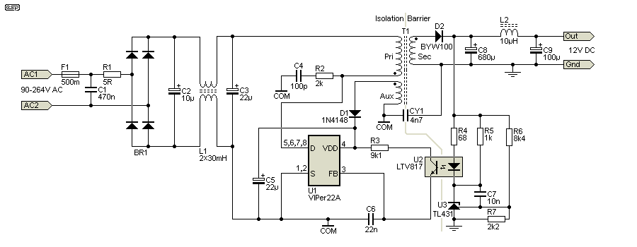
The transformer will be a 'special', designed for a primary inductance of about 2.25mH, with low leakage inductance (no more than 22µH). The turns ratio to the secondary winding will be about 1:0.127 and 1:0.67 for the auxiliary winding. The maximum VDD voltage for the VIPer22 is 50V, and this must not be exceeded. The isolation barrier is created by the transformer and optocoupler, and is bridged by the Y-Class capacitor CY1 (4.7nF). No other capacitor type is permitted in this role. C1 must be an X-Class mains rated capacitor, and C2, C3 are rated at 400V. C4 (100pF) is a 1kV (minimum) ceramic.
Note: There should be a resistor in parallel with the mains input to allow C1 to discharge when the PSU is unplugged from the mains outlet. This eliminates the possibility of the user receiving an electric shock if s/he touches the pins. Normally, it will be at least two high-value resistors in series to ensure that the resistor's voltage rating isn't exceeded. A total value of around 500-600k would normally be used. There's an IC called CAPZero (by Power Integrations) that's designed to connect the discharge resistors only when the AC voltage disappears, minimising wasted power. It may be less than 100mW, but even that may be considered 'excessive' in some jurisdictions. A discharge resistor should also be used with the next example.
Another complete SMPS on a chip is the TinySwitch family from Power Integrations. These are very capable, and for low-power applications such as standby circuits, the auxiliary winding on the transformer can be omitted. This works up to around 1-2 watts output, but for any more the auxiliary winding is still needed.
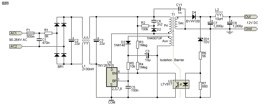
The transformer requirements are similar to that for the VIPer22. The application note doesn't have any values which isn't very helpful. Like the VIPer22, this IC minimises the external parts needed, but the general requirements are the same for any SMPS - full isolation from the mains voltage is essential, as is adequate RF filtering to ensure EMC compliance.
A higher power SMPS (40W for this example) is the 6-pin TO-220 FSDM0565RB from Fairchild (now OnSemi). Like the previous two, these are very capable, and I obtained a couple to repair the power supply of a laser printer (it turned out that the IC wasn't faulty after all, but the printer remained dead). There's the now familiar auxiliary winding on the transformer, and another secondary to provide the two output voltages. Only the 5V supply is regulated, and this is a common approach for multi-output SMPS.
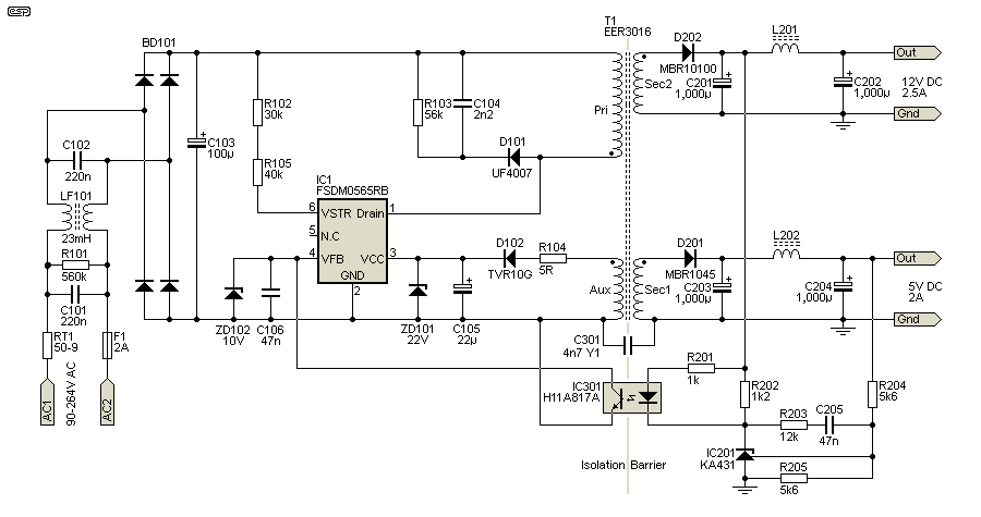
I've reproduced the drawing with the original part designators. Mostly, it's much the same as the other circuits, except the transformer will be significantly larger to accommodate the additional power. The SMPS IC would be attached to a heatsink, and it's a 'full-pack' design (fully encapsulated, including the reverse side) so an insulating washer isn't required, only thermal 'grease'. The output diodes also require a heatsink, as they will dissipate more than 2W each at full power. Overall there's a low parts-count for a 40W SMPS, which can be used for up to 60W in an 'open-frame' design (exposed heatsink) or 70W if it's only used with 230V mains.
This example shows something quite different. Instead of using an optocoupler, the InnoSwitch3 ICs use an internal magnetic coupling system, using a magnetically coupled set of coils (a transformer) to provide the regulation feedback. It also features a synchronous rectifier (Q1) which is a MOSFET used as an 'ideal' diode. This reduces rectification losses. A synchronous rectifier is not recommended for the 12V output.
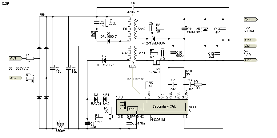
The version shown is only relatively low-power (13W) and it has a low parts count (according to the datasheet). Some may disagree, as it uses more parts than the Fig 4.1 version which also has higher power. However, it is designed to have the highest possible efficiency, and the datasheet claims that R4 can be adjusted to give the lowest no-load power consumption (only 5mW no-load at 230V AC input). The synchronous rectifier gate drive is triggered via R5, which senses when secondary current is available and turns on Q1 via the secondary-side controller.
I've included this example because it shows just how important IC manufacturers (and industry in general) consider efficiency and no-load power to be. Once, no-one thought anything of a SMPS that drew 1W or so when idle, but government regulation and the cost to users of so-called 'phantom' power have demanded better performance. Achieving good results is now something of a 'contest', with each IC manufacturer trying to out-do its competitors for a slice of an ever-growing market.
In Section 1 I mentioned ICs with active PFC, with the one shown from ST Microelectronics. Based on the model number, it appears to be intended for LED lighting applications, where active PFC has become the de-facto standard. Light fittings are used in large numbers, and including power-factor correction is becoming a requirement for many lighting products. Note the very low value of the input capacitor. Where the other designs shown use between 10 to 100µF, in the following circuit it's only 120nF.
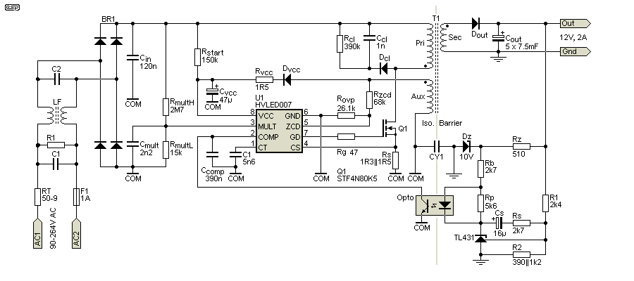
The datasheet doesn't include any values, and those shown were obtained using ST's on-line design software. The software works out almost everything for you, including the transformer. It provides the required parameters that need to be used for the design. The software even calculates the expected efficiency with all losses accounted for. I've not specified the diodes, but they all must be high-speed types (other than the input bridge rectifier).
Transformer Details Parameter Value Primary Inductance (Lp) 700 µH Leakage Inductance (Lplk) 14 µH Primary Saturation Current (Isat) 2.01 A Primary RMS Current 472 mA Secondary 1 Turns Ratio (Np:Ns1) 10:1 Secondary 1 RMS Current 4.13 A Auxiliary Turns Ratio (Np:Na) 8:1 Auxiliary RMS Current 11 mA Secondary 1 Voltage (Vsec1) 12.7 V Auxiliary Voltage (Vaux) 15.7 V
This enough information to allow one to calculate the transformer windings. These values were obtained from the design software as well. The active PFC ensures that the current drawn from the mains is as close to being sinusoidal as practicable, where all other supplies shown do not include PFC, and draw a very unfriendly (to the grid) spike waveform. To understand how this ruins the power factor, see Part 3 - Active Power Factor Correction.
With active PFC, the feedback control loop has to be slow - note the high value of Cs used to stabilise the TL431. As a result, the output capacitance has to be much greater than with the other circuits shown. This means that for acceptable output voltage stability, the main output filter capacitance has to be very large, in this case 5 x 7,500µF (7.5mF) caps in parallel. This is an inevitable compromise when a single IC is used for PFC and power conversion.
I don't know how many ICs are available for flyback SMPS, but there are a great many, by many different manufacturers. Attempting to research them all would be a massive task, and it's one I don't intend to undertake. Some are very similar across different vendors, others (in particular, those that have been in production for some time) may require much more circuit complexity. There are DIP and SMD versions of the same IC in many cases, with the DIP version almost always capable of higher output power due to a larger package and bigger pins to aid heat removal.
There are also many higher power versions, often in a modified TO-220 package with five leads, or sometimes six. The range is bewildering, but many devices you come across are Chinese and there may be zero information available. Some will be copies of other devices, but it's almost impossible to guess which one. The TOPSwitch family of ICs from Power Integrations includes a 3-terminal TO-220 version that incorporates all power and control functions onto a single IC pin (however, it's not recommended for new designs). I've not included one of these, but there's plenty of information on-line.
Several flyback designs use the auxiliary winding for voltage sensing, eliminating the need for an optocoupler to provide feedback. This requires careful transformer design to ensure close coupling of the windings so that output voltage regulation isn't adversely affected. This may be referred to as 'PSR' - primary-side regulation. An example of this type of controller is the TI UCC28632, which uses an external MOSFET. There are so many different options for ICs, regulation system, output power (etc.) that it's hard to choose unless you have a particular preference for one reason or another.
The number of ICs you can get will always be limited to those available from your preferred supplier(s). I generally don't recommend on-line 'auction' sites for buying ICs, as counterfeits are rife. If you're trying to repair an existing SMPS you may find that the IC is no longer available, or is proprietary. In some cases the part number will have been removed, or the only datasheet is in Chinese.
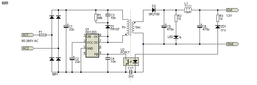
The one shown above comes from a datasheet that is in Chinese, and it's one of the supplies that prompted the article on dangerous power supplies. There is no input filter, and the circuit is about as 'bare bones' as you can get. The one that I have using the DK1203 IC omits both the input and output filter, but it has a somewhat more refined feedback network. What you see may well be what you get if you buy a cheap, unapproved SMPS on-line, and it may (or may not) have an improved regulation circuit. Interestingly, there appears to be no requirement for an auxiliary supply.
You can be certain that as shown, the SMPS definitely won't have approval from any of the appropriate agencies, and it made it to #1 on my 'dangerous' list. The details are shown in the reference [ 7 ].
Transformer design is well developed, and there are guides and design programs to assist with the process. Most are very detailed, and cover the magnetic, electrical and mechanical processes needed to produce a transformer that's safe and (hopefully) easy to wind. There's a lot of information about insulation and material ratings, choice of wire size and mounting arrangements. The insulation test voltage depends on the device class, either Class-I (basic insulation plus power earth/ ground) or Class-II (double/ reinforced insulated). Stand-alone supplies (plug-pack types) can only be Class-II, and must be insulated to very high standards.
The transformer's core loss may be greater than expected because of the rectangular switching waveform. If the core loss is too high, the transformer will get hot. The same will happen if the wire size isn't sufficient for the current. At high frequencies, the skin-effect will cause large-diameter wire to have a higher effective resistance than at DC, and it's common (in high quality transformers) to use multiple strands of thin (insulated) wires rather than a single larger diameter conductor. This complicates the winding process.
Care is needed with the transformer terminations, to ensure that acceptable separation between primary and secondary is maintained within the transformer. Expecting the wire's insulation to withstand the required test voltage (which is 4.5kV RMS or more) is not realistic. All lead-in/ lead-out wires need to be kept separated, and have additional insulation if required. The recommendations for the insulated wire ('magnet wire') vary, with triple-insulated wire recommended for maximum safety. The insulation tape also has to be chosen carefully. Most commercial transformers use Mylar (polyester), but the adhesive must be suitable for the job. Some adhesives may interact with the wire's insulation, although this is (probably) unlikely with modern insulated wire.
Winding geometry dictates the inter-winding capacitance and leakage inductance, both which should be as low as possible. The choice of insulation material depends on the expected maximum temperature. Excessive capacitance and/ or leakage inductance causes high voltage switching spikes and ringing, increasing EMI (electromagnetic interference). It's also important to minimise voltage stress between the ends of a winding where it covers two or more layers on the bobbin. The enamel insulation on 'magnet wire' cannot withstand excessive voltage, and you may also get a corona discharge which will degrade the insulation.
The critical voltage for a corona discharge is around 3kV/mm, so if two wires are 0.1mm apart, the voltage needed is only 300V. This is something that isn't covered in detail anywhere other than in documents protected by a 'pay wall', so I've not been able to access them. In any insulation system, corona discharges can occur at well below the breakdown voltage. These lead to the deterioration and eventual destruction of nearly all insulating materials. Vacuum impregnation is one way to minimise the likelihood of corona (and other) discharges. The transformer's insulation is the most important isolation barrier in the power supply, so it has to be right.
In all cases, creepage and clearance distances must be maintained for the appropriate level of protection. In a PSU that's not enclosed you also have to consider the pollution degree, as any dust or other material that collects on the transformer, PCB or other components may become conductive with high humidity. There's a great deal to consider, most of which takes a lot of research to find.
For any project you may be contemplating, a far safer and more reliable solution is recommended. This involves using a commercial (and fully approved) SMPS and removing the PCB from the original 'plug-pack' housing. It's then installed inside a small 'jiffy box' or equivalent to ensure that live parts are not accessible when installed in the equipment chassis.
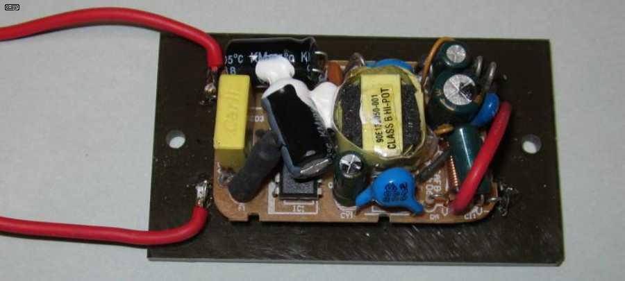
Fig 8.1/2 are my preferred methods, and I've used these supplies in a few my own projects. The PCB for Fig 8.1 was 'liberated' from a commercial (and approved) plug-pack supply, and it was mounted onto a piece of acrylic. The second supply was a small 'in-line' type supply, with a 2-pin IEC mains input socket and a flying lead for the DC output. Both examples can be installed in a small plastic 'utility' box, which protects against accidental contact. The total cost will generally be lower than that to build one, and its safety is as assured as is possible for this class of device. The Fig 8.2 supply is higher power, but it will still fit inside a readily available utility box.
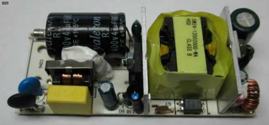
I've also recommended this approach in several projects, as it's a lower cost (plus smaller and more efficient) alternative to a 'traditional' linear supply. However, a linear supply will have a much longer life (50 years and more is not uncommon), where the SMPS has an indeterminate life - it will work until it doesn't. I have switchmode supplies that are well over 10 years old and still work fine, but I've also had a couple that lasted for less than two years (one much less).
One thing that's obvious on both is the input filter, necessary to ensure that EMC requirements are met. These two are well made, and appear to have a generous safety barrier between hazardous and 'safe' voltages. While I can't run tests for isolation (other than using my 1kV insulation test meter), I am confident that both supplies are compliant with all regulations. Both had all of the required safety certifications printed on the original (discarded) enclosures.
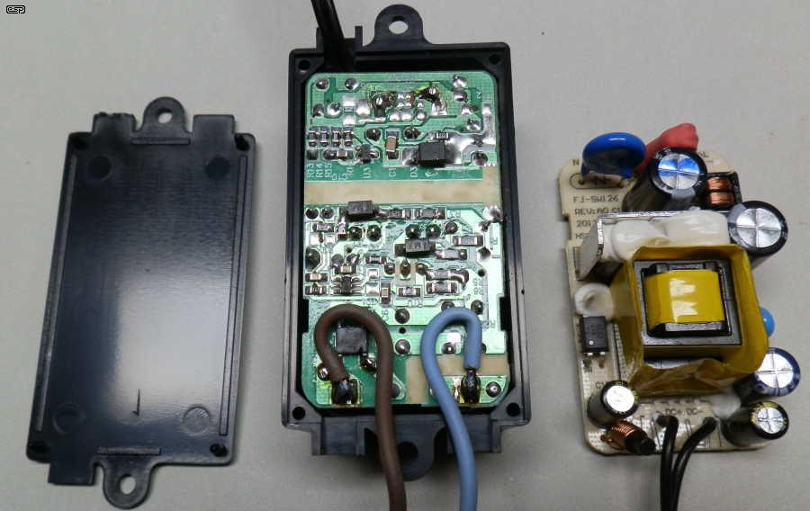
The 12V, 1A SMPS above looks like it was designed for the box it's in. The box is 85 x 38mm, and about 24mm deep. The PCB fits inside perfectly, and it has separated 'ports' for the incoming mains, and a single outlet for the DC wires. This can be installed in a chassis to provide a safe 12V supply for anything that needs it. The supply itself is from a well known reputable supplier, and was liberated from its original plug-pack enclosure. This is as safe as you're likely to find anywhere, and it's small enough to fit into any chassis I'm likely to use it in.
Another alternative is the Hi-Link HLK-PMxx - a small modular supply measuring only 34 × 20.2 × 15mm high. These are 94-265V AC input (50/ 60Hz) and are available with an output voltage of 3.3, 5, 12 and 24V, with a maximum power of 3W. I've not used one of these, but they are low-cost (some are under AU$7.00 depending on seller) and smaller than any other option. They don't have any safety agency approvals though, which is cause for some concern. The only sources I've found are eBay or Amazon. The datasheets claim compliance with major safety regulations, but the products have no printed compliance markings (as required in most jurisdictions).
A switchmode supply provides many exciting ways to cause frustration, angst, poor performance and (of course) smoke. The referenced document [ 6 ] has all the details, but a quick summary is worthwhile.
If the IC has controllable soft-start circuitry, it has to be programmed properly for the transformer used. If the setting is wrong you will experience problems. The exact nature of the issues you may face can't be determined beforehand, as they have too many dependencies. Some of the possible failure modes may not show up initially, or may be affected by the load.
Fault protection circuits can be troublesome if the PCB layout isn't ideal, because even tiny amounts of stray inductance and/or capacitance due to PCB traces can cause havoc. The clamp circuit (resistor || capacitor plus diode, aka RCD [resistor, capacitor, diode]) shown in each circuit reduces efficiency, but it's required due to inevitable leakage inductance in the transformer. However, attempting to reduce the leakage inductance will add considerable time and cost, and if you expect to get below 2% of the primary inductance that's probably unrealistic. Note that some circuits specify a TVS (transient voltage suppressor) diode in place of the parallel resistor and capacitor.
There may also be issues with audible noise, which can be created by the transformer or filter inductors. Vacuum impregnation will keep most of these parts quiet, but adds cost. Also, beware of 'High-K' ceramic capacitors, which can act as tiny piezo 'speakers' if the AC voltage across them is too great. Larger capacitors are more likely to make noise, either by themselves or by flexing the PCB.
Not using a large enough input filter capacitor can lead to ripple breakthrough at maximum output current, and the same will happen as it degrades over its life. The former is easy - use a bigger cap, but the only way to minimise degradation is to ensure minimal losses throughout the system to keep the temperature rise as low as possible. Use 105°C caps whenever possible. Reducing the temperature of electronic components will generally double their life for every 10°C temperature reduction. Also remember that aluminium electrolytic capacitors are notoriously unreliable when used at their maximum rated temperature, ripple current and/or voltage. Using an input capacitor that's too big may cause problems due to inrush current.
Optocouplers are usually considered (by the uninitiated) to be ultra-reliable, but this isn't always true. The LED is subject to 'lumen depreciation' over its life, and the feedback circuit must be able to provide enough LED current to maintain regulation for the life of the product. If the regulation circuit can't supply enough current, the output voltage will rise, either causing an over-voltage shutdown or damaging connected equipment. The optocoupler's CTR (current transfer ratio) is also temperature dependent, and it falls with increasing temperature.
When you buy an approved SMPS, most of the issues mentioned above will have been solved already, at least to a degree that is 'satisfactory'. Expecting perfection is unrealistic, but most of the approved SMPS I've used are 'good enough'. I've had failures (haven't we all?), but most of those I have in my collection have been ok. This mainly excludes cheap 'no-name' types with no approvals, although (surprisingly) some are not too bad.
If you try to build your own, you'll have to do a '1-off' design, debug the circuitry (assuming you can get/ wind a transformer to an acceptable standard), perform perhaps several PCB re-designs and source all of the parts needed. If you imagine for an instant that you'll save money you're mistaken. You will get experience of course, but you're working with live mains and limited test equipment compared to that used by professional SMPS designers. Since you can't get the required approvals (safety and EMC), you'll find that you can't sell it lawfully, and it may even be an offence to give it away!
There are several DIY flyback SMPS that use 1/2 wave rectifiers, presumably to save a couple of cents on the total cost. This is a really bad idea, and isn't recommended for any power level greater than perhaps 0.25W (that's only 50mA at 5V, or 21mA at 12V). Mostly, such low power levels aren't useful other than for a dedicated standby power supply that only has to provide a few milliamps to keep the equipment 'alive' (e.g. to power an IR receiver so the equipment can be turned on via a remote control). Once turned on, the low-power supply isn't needed. Even then, using a bridge rectifier is always a better idea (I really dislike 1/2 wave rectifiers in anything).
Something that should be considered is audible noise. At low power, most of the ICs available operate in 'skip-cycle' mode, where the switching shuts down for several cycles and the output voltage is usually somewhat unstable. This may or may not be a problem for the equipment, but one hopes that the supply doesn't make audible noise. A vacuum impregnated transformer usually ensures no (or minimal) audible noise, and some otherwise very ordinary transformers are completely silent. You won't know until you test it for yourself.
You may have noticed that there are more similarities than differences in the circuits shown. This is inevitable, because the flyback topology doesn't really lend itself to many significant variations. The essential parts will always be similar, but that doesn't mean that you can use (for example) any IC with any transformer. There are requirements for operating frequency, peak primary current and rated power level. While it can seem that the design process is 'trivial', that's not the case at all. Stabilising the feedback loop can be very challenging in some cases.
Much as I'd like to be able to produce a project for a flyback AC/DC converter, I won't do so for many reasons. The first of these is (of course) safety, since making a transformer that's guaranteed to be safe isn't possible because it's home-made. Not everyone can ensure that everything is done perfectly, and I can't even test a prototype to the required standards. Even getting the correct core and bobbin can be challenging, as availability is somewhat variable, depending on your supplier. Because of electrical safety concerns, the circuit would need a PCB, and that's something I'm unwilling to undertake because it promotes the idea of a DIY version.
The alternative to a DIY transformer is to specify a ready-made transformer, but if the constructor can't get it, then the project is over before it even starts. Even ICs can be difficult, as not all suppliers have the same product range, and component shortages make that worse. There are also input and output filters, which require specific parts to perform as intended. I can't do EMC testing, and EMI depends on the construction, so there's no way of knowing if the circuit will kill AM radio reception for you or your neighbours, or interfere with other radio-frequency devices.
Should you decide that you really want to build your own flyback SMPS, you must have 'test points' to allow you to measure as much as you can. That means being able to connect an oscilloscope to all of the important circuit nodes. The supply will almost certainly not be safe to use (especially with no protective earth/ ground), but you will be able to observe and measure its behaviour. During your testing the supply may fail, and unless you get everything right it may even blow up when power is first applied. Rather than being powered from the mains, I suggest that you have an isolated power supply that can deliver up to 150V DC or so at no more than 100mA, so you can run tests safely. You can make adjustments to your design to suit the lower voltage.
The only 'safe' way to work on any mains powered supply is to use an isolation transformer. That means there is no common (neutral) conductor, so contact with one mains lead won't kill you. Contact with both mains leads may be lethal, so the 'protection' provided is totally reliant on your vigilance. Should you get an electric shock, the (IMO mandatory) safety switch won't work, and it could be the last electric shock you ever receive!
While this article looks a bit like a collection of projects, it's not! Ideally, it should be looked at as education, but with no intention to construct any of the circuits shown. These are adapted from manufacturer's datasheets, using the values suggested. I have (deliberately) not included voltage ratings for capacitors or power ratings for resistors, because I really don't want anyone to think that building a flyback SMPS is a good idea.
There are now several approaches to obtaining very low no-load power consumption, but you probably won't be in a position to make use of the ICs used because they are somewhat specialised. A reasonably good SMPS should have no more than ~150mW no-load power draw from the mains, and even this is difficult to achieve. Getting this down to 5mW is possible, using dedicated ICs available from some suppliers. Unless you get everything just right, your supply will likely draw 500mW or more with no load. The SMPS shown in Fig. 8.3 draws 90mW with no load, which is a good result.
After (or before) reading this, I recommend that you also read Reference #7, which covers the hazards in some detail. It also explains why buying from sellers that distribute cheap products directly from Asian manufacturers is a really bad idea.
 Main Index
 Articles Index