

|
| Elliott Sound Products | Voltage Followers And Buffers |
 Main Index
 Articles Index
Contents
A voltage follower, regardless of the technology used to build it, is a current amplifier. A small available current from the source is usually due to the circuit having a high impedance, so it cannot supply enough current to drive the following circuitry. Most of the time, we are concerned with voltage amplifiers, which (as their name suggests) increase the amplitude of the signal. These are used when the voltage from the source is too low to be useful. In reality, the vast majority of circuits combine both voltage and current amplification, although the latter is often not the primary goal. It comes 'free' with the circuit (especially opamps).
When a voltage amplifier is combined with a current amplifier, the end result can be considered to be a power amplifier, having increased both the output voltage and the ability to supply current. In small signal applications, nearly all opamp circuits are actually 'power amplifiers', but they are rarely referred to as such, because the output power is negligible compared to that we normally expect. For example, most opamps are able to supply a few milliwatts at most.
The voltage followers discussed here are only current amps, and do not increase the amplitude of the signal. Indeed, most actually reduce the voltage slightly, with outputs varying between around 0.9 to 0.99 of the input voltage. However, the current from the load can be increased by a factor of between a few hundred up to many thousands of times, depending on the topology of the circuit. In most cases, the 'amplified' current will still only be a few milliamps, although the composite transistors shown in Section 10 can provide many amps of output current from an input of just a few milliamps.
It can be difficult for beginners (in particular) to understand that output impedance and output current are completely different, and one does not imply the other. The purpose of this article is to show the various methods available to get significant current gain, which is essential when the source has significantly less output current than is needed by the circuit being driven.
Examples of devices that need a current amplifier (essentially an impedance converter) are capacitor (aka 'condenser') microphone elements and piezo sensors (common for vibration measurements amongst others). There are many other good reasons to use a current amp/ voltage follower though, because some amplifying devices (notably valves, aka vacuum tubes) have high impedance outputs that aren't very fond of loads that are now common. Most modern-day loads are typically less than 100k, but many are down to 10k and sometimes less.
These days when a voltage follower is needed, it will almost always be an opamp connected as a unity gain amplifier. It can be inverting or non-inverting, with each having its own set of advantages and limitations. The non-inverting connection suffers from (slightly) higher distortion because the common mode voltage is high (i.e. the voltage seen by both inputs at the same time), but with modern opamps this is rarely a problem. The distortion can be measured with (very) good equipment, but there are now opamps that have such low distortion that it's almost impossible to measure it. It is very rare indeed for the distortion to be audible, and if so, it usually means something else is wrong with the circuit.
The greatest benefit of the non-inverting connection is that input impedance is very high, and if you use a FET input opamp it can be very close to infinite. Output current is determined by the opamp you use, as is the DC offset which may be problematical with extremely high input impedance. Noise is usually fairly low, but with high impedances it will be dominated by the noise voltage from the input resistor unless the source bypasses the noise (as happens with a capacitor (aka 'condenser') microphone for example).
Using an inverting opamp configuration solves he common mode distortion problem, because there is virtually none. The inverting connection has the disadvantage that its input impedance is limited by the resistor values used. They can't be too high or noise becomes a major problem for low level signals.
For the most part, this article looks at more primitive techniques used as voltage followers - primarily transistor emitter-followers and JFETs, and the valve (tube) cathode follower will also be discussed as part of the historical view.
While there are some who insist that opamps are somehow 'bad' and that only discrete designs should be used, there is nothing to suggest that this is true of anything other than the most pedestrian of opamps. Even there, a lowly µA741 opamp will have better distortion figures than many discrete designs (although noise and speed are seriously compromised). There are some esoteric circuits that are arguably better than (some) opamps, but at the cost of many parts and significant PCB real estate.
Since I'm not about to build and measure every circuit discussed, the results will be as derived from the SIMetrix simulator. It can be somewhat optimistic in some respects, but because familiar transistors and basic opamps will be used for all simulations, the results will be comparable. I used a signal voltage of 1.414V RMS (2V peak) for the simulations, as this is a realistic operating level for many common circuits.
Opamp circuits will be described using a dual supply, typically ±15V. Discrete followers will generally also use a dual supply, although they can all be used with a single supply if preferred. Eliminating the DC offset is usually best done by adding an output coupling capacitor, and that's generally necessary even when a dual supply is used.
An important point to make is that an impedance converter circuit should ideally be able to source and sink current equally well. If it can't, the output may be asymmetrical with some loads. Sourcing current is taken to mean that the circuit is providing current to the load, while sinking current means that it's drawing current from the load. Any follower should also be able to provide the same peak voltage (positive and negative) to its rated load, and preferably down to the lowest load impedance likely to be encountered (real life is unpredictable).
Simple emitter followers can't usually provide fully symmetrical operation unless their operating current is unrealistically high. In some cases you can offset the output voltage so that there's less voltage across the transistor, and more across the resistor, and that can restore symmetry for a defined load impedance and reduce distortion. However, creating deliberate asymmetry isn't a cure-all and will only work if you know exactly what you're doing.
Be very aware that simple circuits such as emitter followers have relatively poor power supply rejection ratios (PSRR), so hum or noise on the supplies will affect the signal to some extent. Simple emitter followers as shown in Figure 2 will have a PSRR to the emitter circuit of around -27dB, and about -44dB to the collector circuit, with a 10k source impedance. These figures depend on the component values and (especially) the source impedance, so are only a guide.
Of the circuits discussed here, very few are suitable for buffering DC voltages. Because there are DC offsets that can seriously affect the performance of many of the circuits, they are only suitable for AC operation, meaning that there is a requirement for an output coupling capacitor to block the DC component. In many cases, an input coupling capacitor will also be used, especially if the source has a DC potential.
Many single opamps have provision for an offset null potentiometer, so that input transistor DC offsets can be zeroed, allowing the circuit to operate accurately with DC voltages. This is rarely necessary in audio frequency circuits because the DC is removed by a capacitor, but it's essential for high accuracy circuits that include a DC component that must be preserved. Note that there are many advanced techniques to obtain very high accuracy for DC (such as chopper stabilised amplifiers), but these are not covered here because they are specialised (and usually expensive) parts and aren't necessary or desirable for normal audio frequencies.
Note Carefully: While all the circuits shown on this page have their outputs directly connected (with or without a capacitor), if the circuit is going to be used to interface to the 'real world' via a shielded cable, a resistor must be placed in series with the output. If that isn't done, oscillation is far more likely than not, and it may be at such a high frequency that it doesn't show up on a typical 20-50MHz oscilloscope. The resistor needs to be at least 50Ω, and I generally use 100Ω resistors in this role.In some cases it may also be necessary to add a 'base stopper' resistor, directly in series with the transistor's base connection with as little PCB track as possible between the two. The value can vary from as little as 100Ω up to perhaps 1k or more, but remember that a higher resistance will degrade noise performance. Sometimes you can figure out that a base resistor is needed if you discover that audible noise or distortion changes or goes away when you touch the transistor or components connected to it with your finger.
While it may seem unlikely that an emitter follower or unity gain opamp can oscillate, it most certainly will do so if a high Q tuned circuit (such as a length of coaxial cable) is connected directly to the output. Since any oscillation so caused will be RF (radio frequency), it can go unnoticed, but distortion performance will be degraded and in some cases the oscillation may be audible as an audio frequency buzz. The resistor damps the tuned circuit, and makes sure that oscillation will not occur under normal circumstances.
Despite everything I've said above, there are still instances where a discrete design is a better option. If you need higher voltages than can be handled by affordable opamps, or if you need higher output current than can easily be supplied, then a discrete design may be the simplest and cheapest option. This also applies if you need especially wide bandwidth (over 1MHz or so) or other special requirements that aren't met by available ICs. You may never need to build a discrete circuit, but there's no doubt that opamps can't be used for everything.
One factor that has to be understood is the intrinsic emitter resistance (re - literally 'little r e') of a bipolar transistor. This varies with emitter current, and is generally taken to be ...
re = 26 / Ie (in milliamps)
So if the emitter current is 1mA, re is equal to 26Ω. It falls to 2.6Ω at 10mA, and rises to 260Ω at 100µA. This non-linearity is responsible for much of the distortion in any circuit that uses bipolar transistors, and where the emitter current changes during operation (which will be the case in the great majority of circuits). Similar mechanisms exist in all amplifying devices, and despite claims to the contrary, no known amplifying device is truly linear - especially valves!. With JFETs and MOSFETs, one distortion mechanism is the variation of gm (mutual conductance) with drain current, but there are also others that are rather complex and will not be covered here. The design process should always ensure that non-linearities are minimised by using appropriate circuit techniques, not by using 'esoteric' parts.
It's also important to recognise that with few exceptions, the circuits shown here are in their basic form only - they are not optimised for any particular application.
An 'ideal' (i.e. theoretical) voltage follower has an infinite input impedance and an output impedance of zero ohms. Obviously the 'ideal' doesn't exist other than in simulators, but it's still a useful tool during simulation because opamps (in particular) come close enough to the ideal case that any difference is largely academic. The input impedance of a JFET input opamp is usually in the gigohms range, and the output impedance is a few ohms at most. The output voltage is limited by the power supply voltages, and the output current is set by the opamp itself. It's usually about ±25mA or so, but if loaded that heavily the available output voltage is reduced.
There are a few acronyms that you'll find in this article. Most should be familiar, but they are repeated here so you don't have to look them up.
BJT Bipolar Junction Transistor (standard transistor, such as 2N2222 or BC549, etc.)
FET Field Effect Transistor, equivalent to ...
JFET Junction Field Effect Transistor
MOSFET Metal Oxide Semiconductor Field Effect Transistor
CMOS Complementary Metal Oxide Semiconductors (Complementary MOSFETs)
Opamp Operational Amplifier (aka op-amp or op amp)
The basic opamp circuits will be covered first, because they set the goal posts for the parameters that we aspire to. With few exceptions, discrete transistor designs don't even come close to the opamp based followers. The main parameters we are interested in are input impedance, output impedance, and gain. While it's accepted that followers in general don't have gain as such, if the internal gain is too low, then there will be a loss of signal. It's usually less than 1dB even with a valve cathode follower, but it's still a loss of level that will compromise the effectiveness of circuits such as active filters that rely on feedback to get the desired performance.
There is a full discussion about output impedance below, but a word of warning is needed here as well. While a typical opamp may offer an output impedance (with feedback) of less than 1Ω, there is also a limit to the short-circuit current, and the maximum output swing is dependent on the load impedance (and hence the peak output current).
This means that if you use a load impedance that's too low, you will not be able to get the maximum output voltage, and distortion is increased - often dramatically. Most common opamps are limited to a load impedance of 2k or more, but there are also quite a few that can handle 600Ω loads, and a few that can handle even lower impedances. If you need to drive a low impedance, you must check datasheets to verify that you can get both the output current and voltage you need, or the circuit may not be acceptable for your purposes.
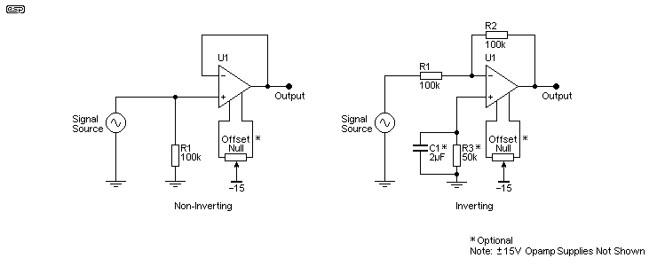
Figure 1 - Opamp Voltage Followers
Figure 1 shows the standard opamp buffers, non-inverting and inverting. Of these, the non-inverting configuration is the most common, and although it does invoke common-mode distortion (because both inputs are driven to the same voltage), it is one of the most used circuits known. A great many ESP projects use non-inverting buffers, and they are particularly common with active filter circuits. The input impedance is set by R1 (100k - although it may be a great deal higher with some opamps), and that's in parallel with the opamp's input impedance.
The offset null connections are optional, and are only necessary if an absolute DC level must be maintained. Pin numbers and pot value vary, so the datasheet must be consulted to determine the proper connections and value for the opamp being used. In most cases the offset null isn't necessary, particularly when capacitor coupling is used.
Minimising DC offset is usually not particularly important for audio, especially when the supply voltages are greater than ±5V or so, because there's plenty of 'headroom' and even a few hundred millivolts of offset isn't an issue. The output capacitor removes the DC component and everyone is happy. However, if you do need a low offset, that's achieved by keeping the DC resistance from each input to earth/ ground equal. This is shown above in the inverting circuit, with a bypassed resistor to earth from the non-inverting input. Its value is equal to the resistance of R1 and R2 in parallel - assuming that the source resistance/ impedance is zero.
The resistor is bypassed by a capacitor so that the resistor's thermal noise is not added to the signal, thereby reducing the signal to noise ratio. This arrangement used to be very common, but most modern opamps are good enough to let you simply earth the unused input (no series resistance). It is rarely necessary to ensure input resistance balance, but if you are designing a high gain DC amplifier then it's advisable to keep the resistance at each input the same.
As noted in the introduction, the main benefit of the non-inverting configuration is its very high input impedance. Even if opamps with bipolar inputs are used, a high input impedance generally only affects the DC offset. There is a measurable input impedance of course, and if you need an impedance greater than around 1 Megohm it's better to use a FET input opamp. Opamp manufacturers don't specify the input impedance directly, because it depends on how the device is used. They do specify the input bias current, and this can be used to work out the DC offset you'll get with a given input resistance to ground. You can also use the input bias figure to work out an approximate input impedance, but it's not always reliable for a variety of reasons.
It might be possible to measure the input impedance, but it will be with some difficulty. The easy way is to add a resistance in series with the generator, and adjust its value until the level has fallen to half (6dB). Assuming that the generator has a negligible impedance (typically between 50 and 600Ω), the opamp's input impedance is then the same as the series resistance. However, since the opamp is used with 100% negative feedback, even a rather basic opamp such as the RC4558 will almost certainly have an input impedance of several megohms. The datasheet claims a typical input resistance of 2MΩ, but in my experience this is somewhat pessimistic. Input bias current is ~50nA (typical).
Should the input resistance be more than 1Meg or so, you will have real difficulties taking a measurement. The opamp's bias current may cause it to swing to a supply rail before you can take a useful measurement. You can use a lower value resistor and calculate input resistance based on a voltage drop. I'll explain this the long way, as that only needs Ohm's law and basic maths, so is more easily remembered ...
Measure the output with zeroΩ in series with the input. Let's assume 1V RMS. Add a variable resistor (a 1M pot for example) in series with the input pin of the opamp, and adjust it until the output voltage falls to 900mV RMS. If the series resistance is (say) 500k, you know that 100mV is dropped across the resistor, and 900mV is available at the opamp's input pin. Make sure that your measurement does not include any DC component of voltage or current.
Iin = 100mV / 500k = 200nA
Rin = 900mV / 200nA = 4.5 MΩ
The series resistance isn't so high that the opamp saturates (swings to either supply rail), but is enough to allow a fairly accurate measurement of the opamp's input resistance under normal operating conditions. A similar technique is used to determine output impedance, which we shall examine later in this article.
Note that some opamps will swing negative if the input resistance (the opamp's bias resistor) is too high, and others swing positive. It depends on whether the input stage uses PNP or NPN transistors. PNP input transistors will cause the input voltage to be pulled towards the positive supply, NPN transistors cause it to be pulled towards the negative supply. Since we are talking about followers, for the non-inverting case the output follows the input.
FET input opamps (JFET or CMOS) draw negligible input current, for example a TL072 is specified for a typical input bias current of 65pA and an input resistance of 1012Ω (1 TΩ). Any attempt at measuring such a high resistance is doomed, because you aren't measuring a resistor, it's an insulator. It's generally safe to assume that most FET input opamps have an input impedance that's much higher than you will ever need for most applications. PCB leakage may easily become a factor well before the opamp itself has any influence.
Of course there will be situations where your circuit may need exceptionally high input resistance, and special construction techniques are required if that's the case. Most of the time, general purpose circuits (especially audio) don't require impedances much greater than a couple of megohms, and ultra-high impedances won't be examined here. For those interested, there is a project showing a 1GΩ preamp (see High Impedance Input Stages / Project 161 for more info.
Inverting opamp buffer stages have a couple of major disadvantages. The input impedance is set by the input and feedback resistors. These must both be the same value for a unity gain inverting buffer. It's inadvisable to make them very high values (> 100k) because noise becomes a serious issue. In general, it's not a good idea to use the inverting buffer for high impedance low-level signals due to the circuit noise. The input impedance is simply the value of the input resistor, and it doesn't need to be measured.
There is also an advantage, in that the input common mode input voltage is close to zero, ensuring minimum common-mode distortion. While this is rarely a problem for most decent opamps where distortion remains at close to immeasurable levels, it's something to be aware of. This is one of many trade-offs that are required in all aspects of electronics design - for every disadvantage, there is usually an advantage, but neither may be of any real consequence for most designs.
The inverting configuration also has a noise gain of 2, so the opamp contributes more noise than a non-inverting buffer which has unity noise gain. As mentioned above, there is a benefit in that distortion is usually lower because there's no common mode voltage, and both opamp inputs sit at close to zero volts regardless of input signal (assuming a dual supply). However, the reduction of distortion is generally rather small with most opamps, and using that as an excuse for not using a non-inverting buffer would be unwise.
What is 'noise gain'? If you examine the configuration of an inverting buffer, you'll see that the feedback and input resistors are just what you'd expect to see in a non-inverting amp with a gain of 2. When the source impedance is low compared to the input resistor, noise is therefore amplified by 2, but the signal is only amplified by -1. The noise gain is simply a measure of how much the noise is amplified compared to the signal. This applies to all inverting opamp stages - the noise gain is equal to the signal gain plus 1.
It's common (or it used to be common) to include a resistor (shown in Figure 1 as 'Optional') in series with the +ve opamp input to ground (R3). The value depends on whether the input is AC or DC coupled. If there's a cap in series with the input, R3 will have the same value as the feedback resistance (R2). With no cap (DC coupled), R3 will be equal to half the value of R1 and R2 - 50k as shown. If R3 is replaced by a short to ground, the DC offset at the output of the inverting buffer will be around 13mV, vs. well under 1mV when the resistor is used. Of course, this depends on the opamp used.
So, while the extra resistor removes much of the input stage DC offset, the resistor must be bypassed with a capacitor to minimise noise. The bypass cap needs to be large enough to bypass noise down to the lowest frequency of interest. If you need response to 20Hz, the cap's reactance needs to be equal to the resistance at one tenth of that frequency - 2Hz. For example, a 50k resistor needs a bypass cap of 1.59µF (use at least 2µF as shown, 10µF is fine). It's unrealistic to expect the cap to bypass 1/f (aka 'shot') noise, so there may be a small uncertainty when measuring DC.
With most newer opamp designs the resistor is not necessary, especially if the opamp has offset null terminals. For audio, it's rarely used because it simply adds more parts for no useful purpose. The output should always be capacitively coupled unless response to DC is a requirement.
The simplest and best known voltage follower is the emitter follower, also known as a common collector stage. The collector is at AC ground potential, because it's connected to the supply rail. These used to be very common in all kinds of audio circuits, but they perform very poorly in almost all respects compared to an opamp. Input impedance depends on the load that's connected to the output, so rather than maintain a high defined input impedance, it varies when the load is added, changed or removed. There's a 0.65V DC offset from input to output, and it needs a DC load from the emitter to ground or a supply rail (which rail depends on whether the transistor is NPN or PNP). The load is most commonly a resistor, but that causes the output drive capability to be asymmetrical. While it can source a reasonable current via the transistor, its current sinking capability depends on the resistor value.
All simple follower circuits have a small loss of level, typically providing an output of between 0.99 and 0.999 of the input level, depending on the gain of the transistor(s) used, the topology and the source and load impedances. Unlike opamps, the input and output impedances of emitter followers are interdependent, so changing one also changes the other. Opamps avoid this by using very high internal gain and lots of feedback, so while there is still some interdependence it's usually so small that you will be unable to measure the difference.
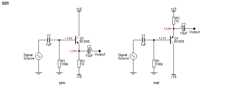
As shown above, the two circuits have a 1k emitter load, and the external load impedance should not be less than 10k if a large output voltage swing is required. If lower load impedances are expected, R2 needs to be reduced, but that reduces the input impedance and increases the quiescent current drawn. With ±15V supplies, this single transistor stage draws more current than 3 to 5 opamps (depending on type), but doesn't perform anywhere near as well. The performance of both circuits is roughly similar, and you can even use both together with the outputs joined with caps to create a complementary emitter follower as shown further below.
With the values shown, the input impedance of the transistor (ignoring the 100k bias resistors) is about 500k with no load, falling to ~450k when the 10k load is connected. Input impedance is roughly the value of the load impedance in parallel with the emitter resistor, multiplied by the transistor's gain (hFE of 500 in my simulation), and in parallel with the input bias resistor (R1). Because of the transistor's bias current, there is 1.8V dropped across R1 (18µA base current) and a little over -2.5V at the emitter due to the typical 700mV between base and emitter of a silicon transistor.
Most of the circuits shown here use a dual supply, but when only one supply is available the emitter follower must be biased so the emitter is at roughly half the supply voltage. The most common arrangement is shown next. As you can see from the voltages shown, the emitter of Q1 sits at a little over 6V rather than the optimum 7.5V. R1 needs to be reduced to 69k to obtain the optimum bias point, but as long as the signal level never exceeds a couple of volts (RMS) the use of two equal resistors is quite alright.
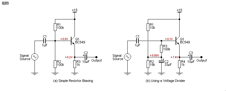
It's important to understand that the use of two resistors as shown in (a) reduces the input impedance. It's now R1 in parallel with R2 in parallel with the transistor's input impedance. Equal value resistors were used here to demonstrate that the emitter voltage will be less than desired. Reduced input impedance can be avoided by either using higher value resistors or the second biasing scheme, using a bypassed voltage divider as the bias supply. The second version has the advantage that any power supply noise is not passed on to the base circuit. The voltage divider (R1 and R2) is deliberately unbalanced to obtain close to half supply at the emitter.
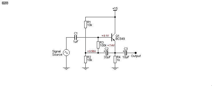
There are many variations on biasing schemes, including direct coupling the base of the emitter follower to the output of the preceding stage. There's also a technique known as bootstrapping, where the emitter signal is fed back to the centre tap of the voltage divider as shown above - C2 connects to the emitter rather than ground. This trick boosts impedance with positive feedback. By ensuring that the AC voltage at each end of R3 is almost the same, its apparent impedance for AC is increased by at least an order of magnitude, but DC conditions aren't affected.
The input impedance of the bootstrapped emitter follower is around 340k, so it should be apparent that R3 has little influence for the AC input. The DC resistance is still 100k of course, so the voltage drop caused by the transistor's base current isn't changed. Bootstrapping has been used in this way for a very long time, and it can even be applied to valve circuits.
Bootstrapping has a couple of downsides though, firstly that there's a 2dB gain boost at 1.5Hz with the values shown. In effect, a rather odd 8 to 9dB/ octave high pass filter is created by the combination of C1, C2 and the associated resistors, and it has a higher than expected Q ('quality factor') that creates a peak before it starts to roll off. The effect (and Q) of this filter depends on the source impedance, so it can be unpredictable in 'real world' applications. With a high source impedance, the amount of boost is reduced, and when the source impedance is 100k (for Figure 4) there's no boost at all. The low frequency response extends to just below 1Hz (-3dB) with a 100kΩ source. This point is rarely raised in most articles you might come across, but it can be a trap if you don't know about the potential for 'interesting' low frequency effects.
Secondly, because the bootstrap circuit uses positive feedback, it will cause transient instability if there is a DC change at the input. Another issue that arises is that the circuit may have a significant settling time, so after power is applied you may have to wait for several seconds (or more, depending on component values) before the DC conditions are stable. This is also due to the use of positive feedback, which causes a damped low frequency oscillation at a frequency determined by the resistor and capacitor values used.
It's essential to build the circuit and test it with your application before you decide that using a bootstrapped input circuit is the best option. Because of the positive feedback, the impedance depends on the signal frequency, and it is also affected by the Miller capacitance of the transistor as well as any stray capacitance, limiting input impedance at higher frequencies.
Although shown with a single supply, bootstrapping can be applied to any variant shown in this article (including JFETs and opamps). For the circuits using dual supplies, only one resistor to ground and one to the base is needed (two resistors instead of three), with the bootstrap cap connected to their junction. This lets you reduce the value of the input resistor to reduce DC offset if you wish to do so. The resistors don't have to be the same value, but to see exactly what happens with any given circuit requires that you build and test it, or at least run a simulation (which will usually be very close to reality).
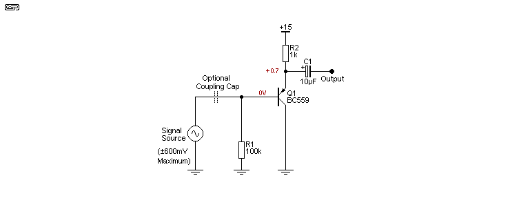
The version shown above is simply too interesting to omit. It has many limitations, but despite that it's used as the input stage for some single supply ICs where the input is allowed to include ground (e.g. LM358, LM386 and a few others). While it might not seem possible, the circuit acts as a normal emitter follower with an AC input that's referred to ground. The input can swing to a maximum of about ±600mV, despite the fact that there is no separate negative collector voltage supply. The circuit relies on the base-emitter junction voltage to provide just enough voltage differential between the collector and base to allow the transistor to function normally.
The circuit is a special case, but can be very useful. It can be DC coupled as shown, or capacitor coupled as with the other circuits described here. When a coupling cap is used between the source and input (shown dotted in the drawing), the base voltage will rise depending on the transistor gain and emitter resistance. With 100k (and using a transistor with an hFE of around 420 for a BC559C), the base voltage will rise to about 2.7V, allowing a considerably higher input (and output) voltage of about ±2.6V (1.9V RMS). As with most other circuits shown here, you will need to experiment. In general, I wouldn't be happy with an input signal of more than around 700mV RMS even with capacitor coupling, because transistor parameter variations could easily cause problems otherwise.
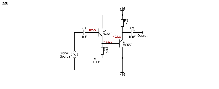
By using a pair of emitter followers of opposite polarities as shown here, the total DC offset is minimised, being reduced to between 100mV and 150mV, rather than over 2V as with the single stages. Performance is similar to the Darlington and Sziklai pairs shown below. The additional resistor (R2, 10k) helps force Q1 to draw enough current to ensure reasonably high gain, and without it the circuit won't work at all because Q2 has no path for base current. Ignoring base offset voltage, the emitter of Q1 will be at -600mV, and this is offset by the base-emitter voltage of Q2 (700mV). They will never cancel perfectly because the transistors operate at different currents, and the DC offset at the base of Q1 isn't compensated so some of it also appears at the output.
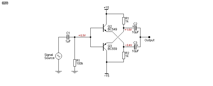
This circuit has the advantage that input bias current is minimised, and if the transistors were identical they would balance out perfectly. Many 'symmetrical' amplifiers use a similar input stage, but true symmetry is not achieved because NPN and PNP transistors will never be perfectly matched. Input impedance is about 200k for the circuit shown (not including R1 and with no load), and input bias current is a little over 3µA, which is significantly better than a single transistor as shown in Figure 2. It has the advantage that output drive is symmetrical, so it can source and sink current (almost) equally well. However (and despite appearances) the circuit cannot drive very low impedances to the full supply rail. With the values shown it can provide up to ±30mA into the load with around 0.5% distortion. The input impedance falls with the load impedance, and is reduced to about 150k with a 1k load.
There are many opamps that can do a great deal better, and they don't require two output capacitors - you can often get away with not using an output cap at all if the offset is low enough.
To increase the input impedance, a Darlington pair can be used. This provides higher overall gain and better linearity, but increases the DC offset at the output. A far better circuit uses an NPN and a PNP transistor in a complementary feedback (aka Sziklai) pair. This arrangement has an internal gain that's similar to the Darlington, so in both cases input impedance is increased, and both output impedance and distortion are reduced. With the complementary pair, the DC offset at the output is also reduced. The circuits are shown below.
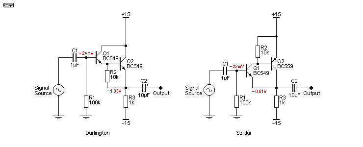
However, there's a small problem with these arrangements, in that the first transistor (Q1) is run at very low current, and this limits the effectiveness of the pair of transistors in both circuits. When operated at low current, the gain of a transistor falls, and this is sometimes shown in the datasheet, although it's often not shown for exceedingly low current (a few 10s of microamps). This problem is partly circumvented by adding a resistor, shown as R2 (10k), and it forces Q1 to operate at a slightly higher current than would otherwise be the case. Input impedance is typically increased to over 4 megohms, although it falls at higher audio frequencies. The Darlington has a higher input impedance, but it falls faster with increasing frequency, and is roughly the same as the Sziklai pair at 20kHz. The HF performance is affected by internal (mainly collector to base) capacitance.
Of the two, my preference is for the Sziklai pair. It has a lower DC offset at the output (which improves symmetry slightly), but it has a certain 'elegance' that is lacking in the Darlington pair. The small amount of local feedback that is inherent with this topology also helps to reduce distortion (albeit only by a tiny amount). Because of the very high transistor gain, the voltage gain is very close to unity - expect at least 0.999 with the values shown.
The circuits shown so far have a resistor to provide the current for the emitter follower. This is cheap, but doesn't provide the best linearity because the transistor's current is constantly changing with the applied signal. For example, with a 1k resistor as shown, the transistor's current changes by 1mA for each volt change of the emitter voltage. Transistors give their best linearity when the current through them is constant, but this isn't the case if a resistor is used to set the emitter current.
A current source will improve the stability of the operating current, but it's not a panacea. The load also demands current, and this causes the emitter current to vary (thus causing re to vary accordingly and introducing some distortion), but the change is usually - and ideally - much less than when a resistor is used. Unfortunately, adding a current source also increases overall complexity and increases the component count. This makes the use of discrete circuits less appealing.
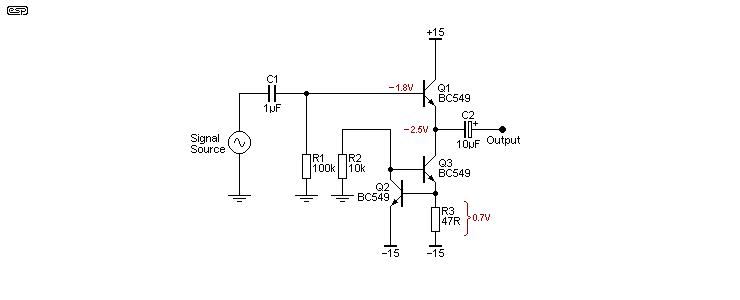
The current source can be used with a simple (one transistor) emitter follower, or with the Darlington and Sziklai pair versions. The current source circuit can be referenced to the positive or negative supply (the latter is shown), allowing it to be used with PNP or NPN emitter followers respectively. It also works with JFETs and MOSFETs, but with those it only improves linearity - input impedance is not affected. The amount of current through the source depends on the load impedance, and for small signal circuits needs to be no less than around 5mA - the circuit shown runs at 15mA to match the others described in this article. 15mA will let you drive up to 20V peak-to-peak into a 1k load using ±15V supplies. However, you will note that the transistor current may still fall to zero if too much output current is expected from the current source. If this is the case, the source current needs to be increased.
While there is definitely a distortion reduction compared to a resistor load, it's likely in most cases that the extra complexity isn't warranted. This is especially true if the peak signal level doesn't exceed around 1/2 the supply voltage (±7.5V for Figure 6). Under these conditions, distortion may be reduced by as much as an order of magnitude, reducing from 0.05% to 0.005%, but is still a great deal higher than a less costly opamp.
Many low power Class-A amplifiers use this technique, and the source current has to equal the maximum peak loudspeaker current, typically up to 2.5A or so for a 20W/ 8Ω amplifier. When a high output current is expected, it's usually not possible to include a large current safety margin. However, for small signal conditions it's easy to ensure that the emitter follower transistor current changes by no more than around ±20% or so. The smaller the current variation, the greater the linearity. This is provided the current is well within the device ratings - running a higher current than necessary can easily make performance worse.
A circuit that is popular is the so-called 'diamond buffer', which uses four transistors. The input impedance of the version shown is 500k, and DC offset at the output is around 145mV in my simulation. Input bias current is less than 2µA. It can source and sink current equally well, and the output impedance is about 10Ω. Because of the push-pull arrangement, it operates in Class-AB, and quiescent current is less than 4mA - this is significantly better than a simple emitter follower, especially when you consider its output drive capability (it can drive a 100Ω load to greater than ±10V peak).
The circuit seems to be generally attributed to the (now obsolete) National Semiconductor LH0002 buffer, which has a circuit that's essentially identical to that shown below, but with some resistor value changes. The datasheet claims distortion of 0.1%, which is acceptable but certainly not in the league of even 'ordinary' opamps. It was designed to be used with an opamp, with the buffer included in the opamp's feedback loop.
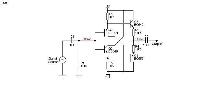
In terms of PCB real estate it's not good - 4 transistors, 4 or 5 resistors (depending on the signal source) and a large output capacitor to allow it to drive low impedance loads. However, there are very few opamps that can come close to it for output current, so it may be worth considering if you have a particularly low load impedance. Other than its high output current, it doesn't come close to an opamp in terms of input impedance, output impedance or distortion, so unless you really need to be able to drive 100Ω loads (for example) it's probably best avoided.
Be aware that if the circuit shown is used inside the feedback loop of an opamp it may be unstable, due to high frequency phase shift within the circuit. This is less likely with an integrated circuit because it can be optimised and all signal paths are very short. For those who think that opamps somehow 'ruin' the sound (hint: they don't) the diamond buffer may be attractive, but these days it should be viewed as a curiosity.
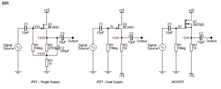
The greatest advantage of using a JFET (or a MOSFET) is that they have extremely high input impedance, limited only by their input capacitance and small amount of leakage. In almost all other respects they are inferior to bipolar transistors, but if you have a need for an input impedance over 10 megohms then you probably need a FET. Where a bipolar emitter follower circuit has a 'gain' of around 0.99, a FET will be a lot worse. A simulation using a BF245C JFET and a 2N7000 MOSFET shows that the JFET gain is 0.903 and the MOSFET is 0.986 - significantly better. Note that the circuits shown below are not optimised, and I used the same value of source resistor as was used for the emitter in the BJT versions above. Ideally, JFETs will be operated at a lower current and they can't drive low impedances as well as bipolar transistors.
In the circuits, the JFET is shown both with a single supply and a dual supply. When a single supply is used, an additional resistor (R2) is needed to bias the FET properly, and it will normally be bypassed (C2) for AC. This connection provides a bootstrap for the input resistor (R1) as a matter of course, and including C2 improves input impedance. If C2 is omitted, the input impedance is around 2.6MΩ, rising to 4.2MΩ when C2 is included. C2 also has a small effect on the gain and output impedance. When it's installed, the FET sees a slightly lower impedance at its source, so gain and output impedance are both reduced slightly.
Distortion for the dual supply JFET measures 0.1% and the MOSFET gives 0.028%, again, a better result. However, the input capacitance of the MOSFET is much higher than the JFET, and the input impedance of both falls as frequency is increased. Measured at 1kHz, the JFET has an impedance of 245MΩ while the MOSFET is only 32MΩ. These values are both significantly higher at lower frequencies, and vice versa. At 10kHz, the JFET is down to 24MΩ and the MOSFET measures 3.3MΩ.
While these figures are fairly respectable, a TL072 (a very lowly JFET input opamp by modern standards) shows an input impedance of 1TΩ (in the simulator and as shown in the datasheet) from DC to well beyond normal audio frequencies, with no loss of impedance until over 200kHz, being down to 900GΩ at 1MHz. No, I don't believe that either, but it's measured with the same simulator as the two types of FET. While somewhat optimistic, it's probably not as far off the mark as you might imagine. Having built a preamp with 1GΩ input impedance using a TL072 I can attest to its performance across the audio band and to at least 50kHz (I didn't measure it beyond that).
The output impedance of a JFET source follower is really nothing to write home about. For the single supply version, output impedance measured 197Ω, and for the dual supply version I measured 133Ω - both are less than awe-inspiring. The MOSFET again does a great deal better at only 25Ω, and this is comparable to a bipolar transistor driven from a medium impedance (around 10kΩ) source.
The performance of JFET followers can be significantly improved by using a current source in place of the source resistor, and adding a BJT emitter follower. This boosts the gain to something closer to unity, and provides a much lower output impedance. These options aren't shown in their entirety, but the version in Figure 12 performs significantly better than its dual supply equivalent in Figure 11 above, even without the added bootstrap capacitor.
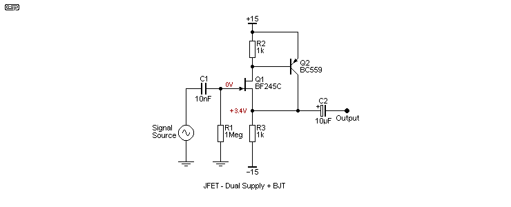
The circuit shown above combines the best of both worlds - the high input impedance of a JFET plus the low output impedance of a BJT. The circuit can be considered a hybrid Sziklai Pair, but with the JFET as the 'controlling' device. The (simulated) output impedance is less than 2Ω, a seemingly impossible feat for such a simple circuit. The same JFET without the buffer not only has much higher output impedance (around 100Ω) but lower gain. A follower is expected to have a gain of unity, but the unbuffered JFET has a gain of 0.83, vs. 0.98 with the BJT. There can be no doubt that these improvements are worthwhile, but performance is still not as good as an opamp.
Regular readers of the ESP site will probably be aware that I rarely specify JFETs for anything where a viable alternative exists. There are several reasons for this, with the main one being that their operating characteristics are extremely variable. Two JFETs, even from the same manufacturing batch, will rarely even be similar, and parametric selection is tiresome. It doesn't help that many of the FETs that used to be common are now very difficult to get, with some of the better devices (especially low noise types) being virtually unobtainable. This makes them rather unappealing for anything more than mundane tasks that can often be accomplished with a bipolar transistor for far less cost.
For a great deal more information on using JFETs, I suggest you read Designing With JFETs. The article describes a simple way to characterise JFETs for maximum drain current (IDSS) and 'pinch-off' voltage (VGS(off)), the two parameters that are the most variable and also the most critical to get a working design.
There is no denying that a JFET provides a very high input impedance, and for this alone they are sometimes the only sensible choice if a FET input opamp can't be used for some reason. If you happen to need good high frequency response, JFET source followers can benefit from bootstrapping, but unlike the example shown for a BJT emitter follower, the drain is bootstrapped to reduce the rolloff caused by the JFET's Miller capacitance between the drain and gate. If the same voltage exists on the gate and drain, it follows that capacitance between them is effectively cancelled until there's a significant phase shift (greater than 45°). This occurs at 197kHz in my simulation.
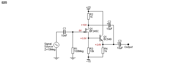
With a 10MΩ source impedance, response without C2 is -3dB at only 22kHz. When C2 is added, this is extended to 215kHz - almost an order of magnitude improvement. The BJT follower is essential to ensure a low output impedance and to minimise loading on the JFET, and without it the bootstrapping won't work. The same technique also works with a MOSFET, and the improvement can be equally significant. This is a somewhat unusual application of the bootstrap principle, and while it may seem to be similar to the system of bootstrapping used in many power amplifiers, it's actually quite different, and serves a completely different purpose.
The input can also be bootstrapped in the same way as shown with emitter followers (and as shown above in basic form), and you can use the two bootstrapping techniques on the same circuit if you need to. A bootstrapped input resistor has the advantage that the resistance (R1) can be a comparatively low value (10MΩ perhaps) while still providing an extremely high impedance to the source. Naturally, the same caveats apply regarding settling time and the potential for unwanted low frequency boost.
Note that any form of 'true' bootstrap circuit can only ever work for AC signals. Because a capacitor is used, bootstrapped DC circuits are not possible. Similar techniques can be used for DC, but they will be active (i.e. using transistors, opamps, etc.) and are significantly more complex.
One circuit that works surprisingly well is shown below, although it's now very dated and doesn't come close to the performance of an opamp. The basic topology is that of a discrete opamp, but simplified to the bare minimum. In the original Wireless World article there was also an alternate version shown, but it doesn't work well so has not been included in my analysis. I've seen the alternate version elsewhere as well, but it still doesn't work as well as the one shown here without significant additional complexity.
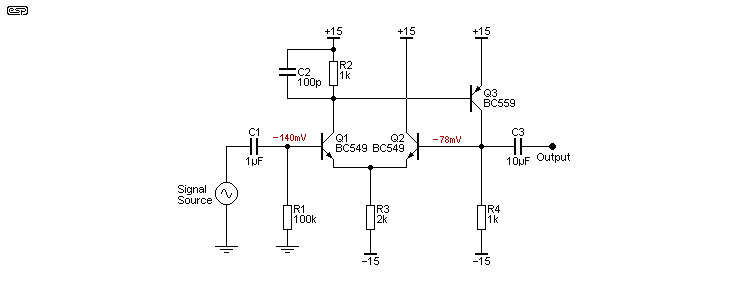
The circuit operates using Q1 and Q2 as a standard long-tailed pair, but 100% negative feedback is applied to the inverting input directly from the collector of Q3. Output impedance is very low at 0.85Ω, and the output voltage swing is limited to +15V and -13.5V, so it can swing to the positive rail, but not the negative. With a ±10V input (7.07V RMS) distortion is 0.06% with no load, and it doesn't change with a 10k load. The load impedance does change the maximum negative swing though, because it is limited by the current that can be drawn through R4.
While interesting (and it performs slightly better than the 'diamond buffer' shown above in some respects), there's really no point because even 'ordinary' opamps will outperform it. Although it's shown with a 100pF capacitor in parallel with R2, this may not be needed. According to the simulator, response extends to over 60MHz, although it's doubtful that would be achieved in practice. However, it will beat almost all opamps in terms of frequency response, so it does still have a potential place in the world.
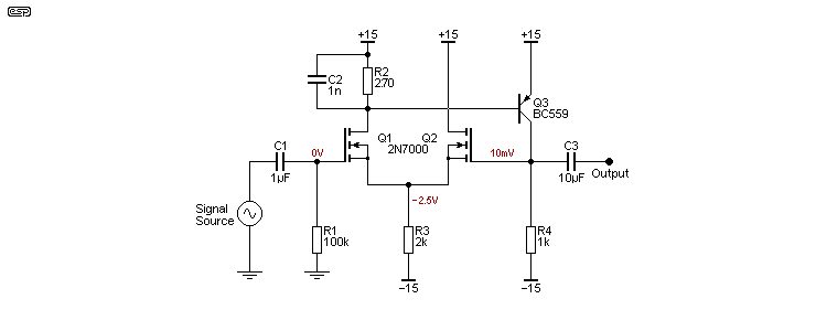
For the sake of completeness, a MOSFET version is shown above. The 2N7000 devices are not particularly quiet, so noise will be an issue at low signal levels. The offset voltage can be trimmed by changing the value of R2. As shown (and simulated), the offset is 10mV, and it can be reduced to almost zero by making R2 around 250Ω. In reality, the MOSFETs will not be matched, so the actual value for zero offset will change - perhaps considerably. The MOSFETs must be in close thermal contact, but even that doesn't guarantee a low and stable offset voltage. Without the coupling caps, response extends from DC to well over 1MHz, and the distortion (simulated) is less than 0.03%.
JFETs can also be used, but the component values need to be changed to obtain the proper operating conditions. With all circuits using a long-tailed pair, the current through each device should be the same. For example, in the Figure 13A circuit, the tail current (through R3) is about 6.2mA, so each MOSFET (or JFET) should draw 3.1mA. Balance is achieved by varying the value of R2.
In the early days of electronics, the valve (aka vacuum tube) was the only option. Unlike transistors and FETs, valves come in one basic format - roughly the equivalent of an N-Channel JFET. There was/is no complementary version, so options were limited. Valves were then (and are now) expensive, and they need a fairly high current to bring the cathode or filament up to operating temperature. Because none of this power is usable by the circuit itself, it's wasted - another expense.
By their nature, valves have a high output impedance, determined almost completely by the plate (anode) and load resistors. The internal plate resistance (rP) also plays a part, but it's not usually considered 'significant' for small signal applications. To get around this, the cathode follower circuit was common, and it was essential in many circuits because without it, the output impedance was too high to be useful.
Cathode followers were poorly understood for quite some time, and many articles were written trying to explain their operation to the engineers of the day [ 4 ]. The referenced article took up four full pages in the magazine! Put simply, the voltage between the grid and cathode will try to remain constant, and if the grid voltage increases, the valve will draw more current from the supply, raising the voltage on the cathode by a similar (but slightly smaller) amount. The converse applies when the grid voltage is reduced.
Valves have very limited gain compared to bipolar transistors, and it was generally accepted that the gain from a cathode follower was around 0.9 (compared to 0.98 or more with a transistor or MOSFET). It's also notable that trying to use tetrodes or pentodes makes no difference, because both plate and screen are at the B+ voltage and the valve will behave as a triode (the screen grid is tied to the plate, which is a triode connection). However, see below ...
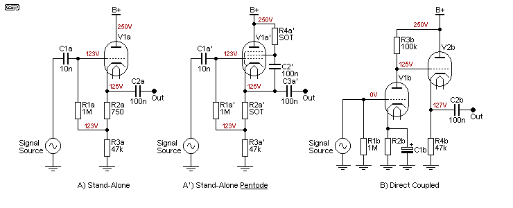
A) shows a cathode follower with an input capacitor (C1a) and biasing resistors (R1a and R2a), which operates as a stand-alone circuit with an input from any suitable source. In many cases, cathode followers are simply directly connected to the anode circuit of the preceding stage as shown in B). That removes the need for C1a, R1a and R2a, and has no downsides, but three components are saved. One always has to be careful with valve circuits though, as it's easy to exceed the maximum allowable cathode to heater voltage because the heaters are nearly always ground referenced. If the voltage is exceeded the valve may be damaged, but even if it survives it may not function properly.
The circuit shown as A' is a special case of using a pentode. The circuit is described in The Radiotron Designers' Handbook, page 324, and explains that if pentode operation is required, the voltage between the cathode and screen must be constant. Suggested methods were an inductor, or the arrangement shown, using a capacitor that's effectively bootstrapped to the cathode by C2a'. This forces the voltage across R4a' to remain constant, ensuring pentode operation. The values shown as 'SOT' are 'select on test'. (My thanks to the reader who alerted me to this interesting design.)
There are several differences between a valve cathode follower and its modern day JFET or MOSFET equivalent. With a valve, operating voltage, impedance and distortion are higher, and both gain and current are lower. Only a single supply is normally used. There was (almost) never a need to have a dual supply with valve circuits, although it could be done if you wanted to - and it was done in early valve based opamps. The design current for the cathode follower shown is about 2.6mA, so the valve might be 1/2 of a 12AT7 or 12AU7 for example. If you wanted to use a 12AX7, the current has to be reduced because they are designed for low current operation (typically no more than about 1.5mA).
Note that R2a can be bypassed, and like the single supply JFET circuit shown above, the input resistor (R1a) is effectively bootstrapped. Because of the low gain of valves, the impedance increase is not as great as you might hope. Unlike JFETs, there is a definite limit to the upper value of the grid resistor, determined largely by the materials used and the geometry of the valve's internal structure. If the resistor value is too high, the valve will attempt to bias itself as the grid collects stray electrons. This is called 'grid leak' or 'contact' biasing, and generally uses a resistor from 2.2MΩ to 10MΩ or thereabouts. The tiny current flow (typically less than 1µA) causes a voltage to be developed across the grid resistor (negative at the grid) which biases the valve. In general, grid leak bias is rather unpredictable and is usually a bad idea, and it should (IMO) be avoided.
If you want to know more about valve circuits in general, see the ESP Valves Index page.
Rather than using a cathode follower to buffer the output of a valve stage, a better option is to use a high voltage MOSFET. They are much cheaper than valves, don't need a heater supply, and they have higher performance. The output impedance will also be much lower and output current higher because you can run a MOSFET with a higher quiescent current than most valves can safely handle. A small heatsink will usually be needed if dissipation is more than 0.5W or so (or the MOSFET can be thermally coupled to a cool part of the chassis using a silicone thermal pad). Suitable devices include the IRF830 shown, IRF820, IRF840, STF3NK80Z, etc.
It is extremely important that any MOSFET follower used after a valve gain stage has good protection for the following circuitry. When the B+ (high voltage) is connected, the output will rise to the full B+ voltage until the valve's cathode warms up, and this can damage whatever is connected to the output. A capacitor is not sufficient - you need to include a resistance and a zener diode clamping circuit to ensure that the output voltage can't exceed ±10V or so (assuming that the following circuit is transistor or opamp based).
Cathode followers are rather ordinary in terms of drive capability, output impedance and linearity. When used at modest signal levels (up to 5V RMS or so), a MOSFET will far exceed the performance you can reasonably expect from a valve. You may expect the gate capacitance (CGS) to cause havoc, but it's effectively bootstrapped by the source itself. For the circuit shown, the -3dB frequency should be at least 100kHz (assuming that the valve has little or no high frequency rolloff).
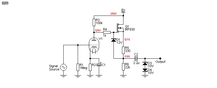
The value of the valve's cathode resistor and bypass capacitor (R2 and C1) haven't been shown because they depend on the valve used, and voltages shown are typical. With the MOSFET resistor values given, the AC output of the MOSFET follower is about 0.98 of the input, and is significantly better than a cathode follower in this respect. Without R4, there is virtually no signal loss at all, but there is also no current limiting. The current limit is around 25mA with a 330Ω resistor. This allows more than sufficient drive to following stages, but limits the damage that can be created with high signal levels.
Output impedance is 330Ω, and is based almost entirely on the value of R4. If R6 is 22k as shown, it should be rated for at least 1W, and the MOSFET needs a small heatsink because it will dissipate a little over 700mW with a 250V supply. Increase the value of R6 if you don't need the drive capacity provided by the 22k source resistor. Output impedance is not affected if you change the value of R6, but the ability to provide a high level signal into low impedances is reduced. The circuit above can provide well over 5V RMS into a 2.2k load impedance.
Linearity can potentially be improved further by including a current source load for the MOSFET, but that shouldn't be necessary for most applications. The added complication is unlikely to provide any audible benefit, and if not done well may do more harm than good. See Project 167 for more information about protecting the following stages, and there's also a muting circuit that can be added.
Most regular readers will know that I am not a fan of using 'vertical' MOSFETs (HEXFETs or other switching types) for linear circuits. This is an exception, because they are well suited to use a followers operating at high voltages. They are almost too perfect in this role, but at least you will know that any distortion comes predominantly from the preceding valve stage. Distortion as simulated is less than 0.01% with 7V RMS output and a 22k load at the output. A cathode follower will hard pressed to even come close to that, regardless of the valve used.
As a side-note, you can eliminate many of the protective parts if the MOSFET follower is used to drive a tone stack (in a guitar amp) or is used internally with other valves. For example, MOSFET followers are ideal to drive the grids of output valves, providing far greater bias stability. They also have no problems driving the grids positive (Class-AB2), which can have some decidedly adverse effects when a valve drive circuit is used. The zener diode and gate resistor are mandatory, but the limiting resistor (R4) and zeners are not required. The protection is intended to stop the valve stage(s) from destroying transistorised equipment (including opamps).
Taking a measurement of output impedance is often very difficult. This is especially true when the output impedance is extremely low, because your measurement will include losses in test leads and relies on the accurate measurement of small voltage changes. First, measure the output voltage with no load, then apply a load of known resistance and measure the voltage again. With most circuits, the voltage used must be small or the circuit will distort, which of course ruins the measurement.
For most of the circuits described here, you can use a voltage of 1V RMS, and the load resistance should be such that the output voltage falls by a measurable amount (around 100mV is usually alright). Note that this will not work with an opamp, because the output impedance is exceptionally low (usually well below 1Ω) but current capability is limited.
It is very important that you understand that you can have a low output impedance, but not the ability to drive an external load to full voltage. These are two different parameters, and one does not imply the other. A circuit can be designed to have high output impedance but supply a high current, or to have a low output impedance but only supply a small current (such as an opamp). Likewise, a circuit can also be designed to have low output impedance and drive a high current, and an audio power amplifier is a perfect example of this.
While the procedure shown below assumes a voltage drop of 100mV and an open circuit output voltage of 1V, you need to substitute the actual values you use. It will not always be possible to drive 1V into a load that is low enough to obtain a measurable voltage difference, depending on the circuit topology and its output current capability. You can also use a fixed resistor instead of a pot, and simply adjust the values in the formulae to suit.
Measure the output voltage with no load on the output. Let's assume 1V RMS. Add a variable resistor (a 1k pot for example) as an output load, and adjust it until the output voltage falls to 900mV RMS. If the load resistance is (say) 400Ω, you know that 900mV is dropped across the load resistor, and therefore 100mV is 'lost' within the circuit itself due to its output impedance. Make sure that your measurement does not include any DC component of voltage or current, and that the output remains undistorted. If the output clips (distorts) when loaded, the measurement is invalid!
Iout = 900mV / 400 Ω = 2.25mA
Rout = 100mV / 2.25mA = 44.4 Ω
This works well with most output impedances, provided they are not too low. In some cases (such as with opamps) it will be almost impossible to measure a reasonable voltage change, even with an unrealistically low value load resistance. The technique therefore can't be relied upon in all cases because it's not possible to measure the voltages accurately enough. With an opamp, output impedance/ resistance is reduced to near zero because of the large amount of feedback.
In a feedback circuit, the output impedance is roughly equal to the internal output resistance divided by the feedback ratio ... provided there is sufficient feedback. For example, an amplifier may have an internal impedance of 1k and a gain of 1,000 (60dB), and if used with 100% feedback (a follower) its output impedance will be 1Ω. However, its ability to supply current to the load is limited by the internal resistance/ impedance, and not the value obtained after feedback is applied. The hypothetical amp just described cannot provide more than ±15mA when powered from ±15V supplies, even though its output impedance is only one ohm. Note that this is a simplification, and while it's fairly accurate for some topologies it is at best a crude approximation.
As already noted, the measurements must exclude any DC component and the signal level must be low enough to ensure that there is no clipping or other distortion. In many cases, the output impedance will be frequency dependent, and this will always be the case with opamps. While output impedance may be less than 1Ω at 1kHz, it will be considerably higher at 100kHz. Typical opamps will have an output impedance of up to 10Ω (sometimes more) at 100kHz, because there is less available feedback due to the opamp's internal frequency compensation.
This is not usually a major issue though, and it's certainly not a valid reason not to use an opamp unless you are working with high frequency circuits. In such cases, it's usually necessary to use discrete circuits because opamps are mostly not intended for use with frequencies much above 50-100kHz. There are exceptions of course, but they may be rather costly and a discrete solution can sometimes work out better all round.
I don't propose to cover high current followers in any great detail, because they are already explained in various other articles and projects on the ESP website. High current versions are typically used in the output stages of power amplifiers, and can be simple complementary Darlington pairs, Sziklai pairs or in some cases a triple (three devices in cascade), and using various mixtures of NPN and PNP transistors. There are many combinations, and it is hard to provide the detailed analysis that each deserves in a short article.
Instead, I will show some of the common variations, purely for interest's sake. If you want to know more, you will need to perform your own analysis because the choice of transistors determines how well each version will work in any given configuration. The selection of devices depends on the application, frequency range, voltage and current, and given the number of transistor types available, the number of combinations is truly vast.
In the drawings below, resistors between individual transistor base-emitter junctions are not shown. For high-current triples, Q2 could have an emitter-base resistor of around 220Ω, and Q3 might use 22Ω, but these values need to be determined by the application and to suit the devices and intended purpose. Higher resistances can increase the turn-off time, and lower values draw more current. This is part of the design process, and each case will be different.
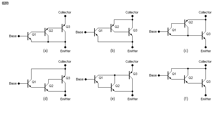
There are six possible connections of devices to create an NPN triple, and the transistor types will be selected as needed to create the versions shown. Their PNP equivalents increase the number of possibilities by another 6 - 12 different configurations in all. I've not included any type numbers because they will vary with the application. Their voltage rating must be greater than the total voltage that may appear across them, and they need to be graded with the lowest current device as Q1, a medium current device for Q2 and a high current type for Q3. As noted above, resistors (not shown) are nearly always be essential between the base-emitter junctions of Q2 and Q3, with values usually selected to minimise the transistor turn-off time.
The version shown in (b) is used in the P68 subwoofer amplifier project, but it uses a high power transistor as Q2 and a much lower than normal base-emitter resistor for Q3. The thermal stability is very good indeed, partly because Q3 is turned off under quiescent conditions. This is a 'special' application of a triple connection.
Note that in every case shown, the input transistor determines the effective polarity of each combination. The remaining transistors are then arranged as Darlington or Sziklai pairs as shown in the drawing. Of the six variations, (a) and (b) will have the best thermal stability, because there is only a single base-emitter junction between the base and emitter of the triple. It follows that (f) will be the worst, because there are three base-emitter junctions in series. The remaining three have two junctions in series, and if possible it's better if the final transistor (Q3) doesn't have its base-emitter junction involved, because the temperature of the final stage is nearly always subject to the greatest variation because its dissipation is the highest.

Because NPN and PNP output transistors will always have small differences, it can be helpful if both sections of a push-pull emitter follower output stage (as used in most amplifiers) can be made to be as similar as possible. The above circuit is not common, and it's not one that I've used in any of the published designs. However, it does have very good linearity, and the only difference between an NPN and PNP stage is the driver transistor. Although the drivers will not be identical, there is likely to be less variation between them than with the output devices. Note that transistor types and resistor values are a suggestion only, and many different types can be used.
The only power amplifier that I know of that uses this arrangement is Bryston (albeit with some variations), but it's inevitable that it's also used by others. Over the years I've looked at hundreds of different output stage circuits, and this is probably the most impressive, but of course it does come with a cost penalty due to the requirement for four output devices in a push-pull output stage. While it performs very well, it's very doubtful that there is the slightest audible difference compared to a 'traditional' output stage.
It should be fairly obvious that for small signal audio frequency applications, it's almost impossible to beat an opamp with any discrete option. Some are fairly good if you work at it, but the PCB area needed is a great deal more than that for an integrated circuit. FETs in general are a good option if you need an exceptionally high input impedance, but again, a FET input opamp will generally have far better performance than a discrete circuit. However, the noise performance of FET input opamps is usually not as good as bipolar types, and a low noise JFET may be a better option where noise performance is critical. There are some benefits to using MOSFETs, but their noise performance is usually a limitation so using them at low levels isn't usually a good idea.
Power amplifier output stages nearly all use emitter follower output circuits, most commonly Darlington or Sziklai pairs. In some cases you will see 'triples' used, having three transistors in a cascade arrangement. There are many different options, and section 10 gives a brief overview only. These circuits are designed for high voltage and current, and are not generally used for small signal applications.
Given the fact that even a simple Darlington pair may not perform as well as expected due to the very low current in the first transistor, it would be rather pointless to add yet another transistor which would operate at perhaps only a few microamps. It's gain (and its contribution to the circuit) will be well below expectations and it's essentially a waste of a transistor.
Be aware that most of the circuits were simulated using BC549C (NPN) and BC559C (PNP), and while any suitable transistors can be used, performance depends on the hFE of the transistors that you actually use. Lower gain devices will create greater DC offsets because their base current will be higher, and vice versa. Unlike opamps, the performance of the simple discrete circuits described depends heavily on the device(s), and you can easily run into problems if the gain is much lower than expected. If you build any of the circuits shown here, they will all work as described, but you may find that the DC voltages are different due to transistor(s) with higher or lower gain than used for the simulations.
Hopefully the reader has more information than before, and is aware of the limitations or potential benefits of simple circuits. There are few reasons in any audio frequency circuit to use an emitter follower these days because the performance will never come close to an opamp, and there is little or no cost saving. The DC offset is always going to be a problem, and making it 'go away' is far more trouble than it's worth. However, some circuits will benefit by not using an opamp, and the variations shown provide an insight into the likely advantages for specialised applications.
 Main Index
 Articles Index