
|
|
| Elliott Sound Products | Balanced Line Driver with Floating Output |
 Main Index
Articles Index
Main Index
Articles Index
The article presented is a contributed design by Uwe Beis. Uwe has built and tested the unit as shown, and although more complex than the balanced line drivers and receivers presented in the original versions in the Project Pages (see Project 51 for details), it also has better performance.
However (and this is important), the sensitivity to component tolerance is high, and thermal drift will cause the circuit's characteristics to change. It is very important that Uwe's recommendations are followed closely with regard to the tolerance and type of resistors used. I have simulated the circuit, and also built one using 5% carbon film resistors to see just how far off the circuit would be. Although it worked (after a fashion at least), the balance and frequency response were quite different for each output. After trimming (using a pot, and experimenting until I found the best spot for it), the performance was excellent, but just heating any of the 10k resistors with my fingers was enough to disturb the balance.
Metal film resistors are very much better than carbon in this respect, and are essential in a circuit such as this.
Additional testing and simulations of the circuit have revealed that there is a sensible trade-off that can be made, simply by increasing the values of 2 resistors. Although the modification degrades the 'perfect' balance, in reality there is only about a 0.4dB loss of signal when the circuit is connected in unbalanced mode, and this is well within the acceptable range.
The simplified version requires no adjustments. Mine uses an unbalanced input, but a balanced input can be added in the same way as with Uwe's circuit. Generally, an unbalanced input will be the most common, since if the internal circuitry is already balanced, there is little need to do it again. See Project 87 for all the details.
The following is Uwe's original material with a very small number of changes. Note that I have made minimal corrections to the grammar - Uwe is from Germany and his English is extremely good. You will still see some evidence of his origins, but to remove all of these would be to lessen the value of the original text (IMO anyway)  .
.
There are a few things that must be understood about balanced circuits, and I must thank Bill Whitlock (from Jensen Transformers) for pointing out a couple of things. I have discussed both points elsewhere, but they definitely bear repeating here.
Firstly, it is commonly (but very much mistakenly) assumed that signal balance is important, but this is not correct. In reality, it doesn't matter at all if a balanced line has all its signal on one lead, and none on the other. What is important is impedance, and the signal leads of balanced lines must have the exact same value of impedance to earth/ground/common at all frequencies of interest. Ideally, this should be as high as possible for both the send and receive circuits. The InGenius® IC (licensed to THAT Corp.) is a solution that provides a much higher impedance to earth than normal balanced line receiver circuits, and it's worthwhile to have a look at the PDF to understand all the reasons.
In reality, balanced receiver circuits are extremely hard to get right, and all active solutions have a limited impedance, often made worse by the addition of capacitors to reduce EMI and/or high frequency noise. Bill Whitlock says "Transformers outperform all conventional input stages for one very simple (and, to me, obvious) reason: transformers have incredibly high common-mode input impedance. In the real world, simply matching these impedances is not enough - they must also be very, very high. With transformers, they are inherently in the area of 50 MΩ at 50 or 60 Hz, and rejection is so high that it became taken for granted ... and seemingly, everyone who ever knew why either forgot or died! Ordinary balanced line receivers have common-mode input impedances in the area of 50 kΩ ... a factor of 1000 less than a transformer (or the InGenius® input stage)."
Secondly, send circuits ('transmitters' if you like) should also have a high impedance to earth, and the circuit shown here does just that. However, it must be understood that the circuits shown are useful, but only to a limited degree. While there is no doubt that the circuit performs well, it is easily disturbed by cable capacitance and can become unstable. Because it uses positive feedback to achieve the high effective impedance to earth, it doesn't take much of an imbalance somewhere to cause oscillation - certainly something that should be avoided.
Ultimately, there is no active balanced send or receive circuit that can match a good transformer - this does not include $20 mic transformers you can purchase from retail electronics outlets! As noted above, the windings of (good) audio transformers have an extraordinarily high impedance to earth unless the centre tap is earthed - generally a very bad idea. If you need to provide phantom power via the transformer centre tap, this ruins the inherent high impedance, but the far end will be a microphone, and is floating. A low impedance to earth is not such a great concern then, as there is no earth reference at the far (microphone) end, other than the mic body which is connected back to the mixer anyway.
It is very important that the true principles of balanced lines are understood properly, but this is often not the case. Many people concentrate on signal symmetry, but neglect the requirement for a very high common mode impedance and/or impedance matching of the two inputs or outputs. Note that this does not imply that input and output impedances be matched, because doing so reduces signal level by 6dB and may overload send amplifiers - whether opamp or transformer based. Transformers provide an almost perfect match when the input or output winding is floating, and will nearly always give the best results in harsh conditions.
Predictably, most people shy away when they see the prices, so opt for (often simple) active circuits instead. Under relatively benign conditions with no heavy interference sources this is often quite alright, and works just fine. Just remember though - just because you have a balanced line, this doesn't mean that you'll get no noise. Oh, and I must point out that balanced lines don't sound 'better' unless better is defined as lower noise or interference. If so (and you get the expected results), then it really is 'better', but mostly there will be no change if your system is already quiet.
In the professional audio industry analogue information is transmitted as a balanced signal over symmetrical cables. The big advantage of this method is that interferences of the signals by ground loops can be totally eliminated. To balance device-internal signals, where they are usually unbalanced, transformers are often used. Transformers have another very welcome side effect: They can completely galvanically decouple source and destination, i.e., there is no ground loop. They are not just compensated, in fact they do not exist any more. One transformer, either at the output or at the input, is sufficient for that, but professional equipment usually uses transformers at its inputs and outputs.
It is well known to use electronic circuits instead of transformers to balance signals at the outputs or to unbalance them at the inputs. The advantage is that this is cheap, small and works easily from DC up to very high frequencies. One major disadvantage is that they cannot handle voltages - particularly common mode voltages - greater than their operating voltage. Rod has written some more explanation about balanced signals in his project 'Balanced Line Driver'.
From here on we should discriminate the difficulties between balanced inputs and outputs.
The line receiver Rod describes is a single op-amp one. It is derived from the basic differential amplifier circuit. Its inputs are not totally symmetrical, i.e. signals at the -In 'see' a lower impedance than those at +In. Furthermore signals at +In are 'visible' at -In while vice versa this is not the case. For higher performance the following circuit is often used ...

Figure 1 - Improved Balanced Line Receiver
Both inputs may be directly connected to the incoming signal - there are no resistors in between. This improves noise performance so that this circuit is well suited for microphone preamps. Furthermore there is no feed-back from the output to any input so that the inputs may have any input impedance up to nearly infinite. The common mode rejection ratio is determined by the precision of the resistors R and will be about 40dB with 1% resistors. With only one additional resistor RGain the gain can be increased without decreasing the common mode rejection ratio. Or, in other words, the ratio between differential and common mode gain is further improved.
Another improved version can be found in project 66, which is based on a dual transistor differential input.
All in all, balanced line receivers are quite easy to realise with little effort. With the exception of the limited common mode range they easily can come close to the performance of transformer coupled inputs. They are no challenge - so I do not want to discuss them here further.
The line driver Rod describes in his article is quite simple too. There is nothing to grumble at ( ), but there is one essential difference between an output like the described one and a transformer coupled one: The common mode output resistance. A common voltage applied to the output will cause a considerable common mode current into the outputs - the output is not floating. Example: The differential output resistance in his project is 2 × 220Ω = 440Ω. If you apply a common mode voltage U at both outputs, a current of 2 x U / 220Ω will flow, i.e., the common mode output resistance is 110Ω (1/4 of the differential output resistance).
Or, another and more important point of view: With transformer coupled outputs you may short either output to ground or apply any voltage there - you will still have the full output voltage across its output ports. If you do this on one output of the simple push-pull amplifier it will not affect the other one. You can even connect several transformer coupled outputs in series and by this way sum all output voltages. This, of course, is not possible with a push-pull amplifier output stage which 'looks' like a balanced output with a centre tapped earth reference.
I call transformer coupled outputs 'floating outputs', because by nature they have a high or infinite common mode output resistance. So I was looking for a transformerless amplifier with floating outputs, and this is where my story starts. (Even though I'm afraid there is nobody out there raising his hand and shouting "Yes that's it! That's what I was always looking for!")
I must admit I never really investigated in circuits to be found in literature or in the www, because on one hand I very soon had an idea myself for an appropriate circuit and on the other hand I cannot remember ever having seen anything like this before. I have since seen the schematics for the Analog Devices SSM2142 which uses almost exactly the principle described here and the complement from THAT corporation, the THAT1420/30. I should also mention the Maxim MAX435, a so-called 'Wideband Transconductance Amplifier with Differential Output', which is somewhat similar but somewhat different too. At least it has a floating balanced output.
My basic circuit not only has balanced outputs but balanced inputs too and looks like this ...
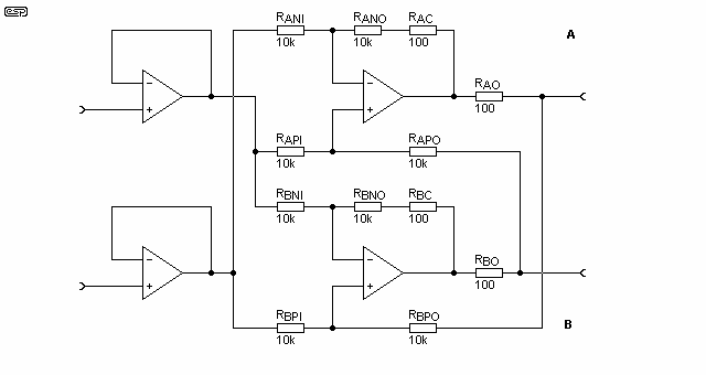
Figure 2 - Basic Form of Balanced Line Driver
Explanation of the indices used:
A, B (RANI): A: 'Upper' ('positive') resp. B: 'lower' ('negative') half N, P (RANI): Connected to the negative (N) resp. positive (P) input I, O (RANI): Connected to the input (I) resp. output (O) op-amps C (RAC): Used to compensate RAO resp. RBO
No bias resistors are shown. The input stage is used to buffer the input signal so that the inputs may be dimensioned for almost ideal properties while the actual line drive is supplied with the required low impedance source.
The whole amplifier, as it is dimensioned here, has a gain of 1. The same amount of voltage across the input terminals appears across the output terminals. This remains true if any output terminal is supplied with any voltage - like transformer coupled outputs do (provided both output voltages stay within the supply voltage area of course). This is a consequence of the fact that the common mode output resistance (RCOut) is high.
The differential output resistance (RDOut) is low, but not zero. It is determined by the resistors RAO and RBO and equal to it. In fact, RCOut and RDOut (the output resistance in differential mode) are coupled at each other by the precision of the applied resistors. As RDOut does not need to be very low and RCOut should be as high as possible, it seems obvious to start with a reasonable differential mode output resistance (RDOut = RXO) of 100Ω.
As mentioned, it is obvious that the precision of the resistors must have a certain influence on the performance of the whole circuit. But what is 'the performance' of such a circuit?
The primary target obviously is a high RCOut at a given RDOut. But at least three side effects must be kept in mind:
A common mode input voltage shall neither be visible at the outputs in common output mode nor in differential output mode (just like with transformers). The 'Common to Common Mode Rejection Ratio' (CCMRR) and the 'Common to Differential Mode Rejection Ratio' (CDMRR) tells about that. Furthermore a differential input signal shall not be visible at the outputs in common output mode. I call this 'Differential to Common Mode Rejection Ratio' (DCMRR).
Of course differential input signals shall be visible at the outputs in differential output mode - this is simply called gain and by design always so close to the desired value that it does not need to be discussed.
Now we know one 'primary target' (the common mode output resistance RCOut) and three 'side effects' (CCMRR, CDMRR and DCMRR) to characterise the performance. I presume two more properties 'gain' and 'output resistance' as sufficiently precise given by design. I neglect other side effects and all input properties.
Now we can restart with the perception that it is obvious that the precision of the resistors must have a certain influence on the performance of the whole circuit and to find out this performance.
I could have tried to put the whole circuit into formulas and to solve the formulas in a way, that the influence of varying resistors on our target RCOut is directly visible, or I could have done this by simulation. Unfortunately my Pspice evaluation version does not support circuits as complex as this one. So at my first approach I preferred to measure the performance in a real circuit. Later I learned more by doing simulations, but I will come back on this later.
For my experimental circuit I thought about how to select the resistors. It seemed obvious that all ratios RXYI / RXYO had to be the same (replace X by A or B and Y by P or N). Furthermore all sums RXYI + RXYO had to be equal. At last all RXO and RXC should be the same.
But you cannot buy parts with equal values, so you have to live with similar ones. I bought 12 resistors with 10 kΩ and 4 with 100 Ω, all specified with 0.1%. The cost of each is approx. $US0.20. I intended to select them so that the sums RXYI + RXYO are as equal as possible. Fortunately I have a 4 1/2 digit multimeter so that I could measure out 4 pairs of 10 kΩ resistors with difference of the summed resistances less than 2 Ω. In order to meet the required equality of the ratios RXYI / RXYO I added three 10 Ω 15-turn trimpots. The result was the following circuit:

Figure 3 - Balanced Line Driver
Why RAOG and RBOG? With ideal parts the output resistance RCOut becomes infinite. With real ones it may become either positive or negative. If RCOut is negative, the outputs run to one of the supply rails and remains there - the circuit does not work properly, it is unstable. Thus RAOG and RBOG are introduced: RAOG parallel to RBOG must at least be lower than -RCOut to guarantee stability. But RAOG and RBOG also improves symmetry of the output signal, and the lower RXOG / 2 is compared to RCOut, the better the output is balanced. At the end, an extremely high RCOut (without RXOG) is only good for a reasonable RCOut (including RXOG) combined with reasonable common mode rejection ratios. Which explains why I declare a high RCOut as the primary target. Making the output means that both outputs have to carry the same voltage (but with opposite signs of course) in case they are open.
The trimpot ROFFS is introduced to reduce the remaining common mode DC output current to zero. Particularly without RAOG and RBOG the remaining common mode DC output voltage caused by the current is extremely high, and just 'a sharp look' at the trimpot may cause a difference of several volts.
During our discussions Rod gave me the hint to try SIMetrix Intro as a simulator. SIMetrix was able to simulate this circuit and with this means I discovered an essential relationship between RCOut, RDOut and the resistor tolerances:
Have a look at the schematic in Figure 2 and note that both op-amps are connected in a loop. Under ideal conditions the loop gain GLoop is exactly 1. By the simulation I found out that the common mode output resistance RCOut can be calculated as RCOut = 2 × RDOut / (1 - GLoop). As RCOut shall be as high as possible, GLoop has to be as close as possible to 1. A loop gain of 1.01 results in a negative RCOut of -20 kΩ must be compensated by RAOG || RBOG < 20 kΩ to maintain stability, but for balancing reasons RAOG || RBOG should be << 20 kΩ. To guarantee |RCOut| >= 20 kΩ GLoop must be between 0.99 and 1.01. Keep in mind that there are 8 resistors and their deviations that influence GLoop!
That looks difficult, but on the other hand a Monte Carlo analysis teaches that with resistor tolerances of 1% (which theoretically could result in loop gains between 0.99^8 = 0.92 and 1.01^8 = 1.08) |RCOut| will be > 20 kΩ (2 × RDOut × GLoop) as desired in more than 99% of all cases. Under these circumstances I would recommend RAOG = RBOG = 4.7 kΩ, which is a fair compromise between the resulting symmetry and the common mode output resistance.
The experimental board
I built the circuit in my favourite way on a Vero square pad board. I observe special rules for that and I would like to write more about it, but not here. I am quite convinced it looks professionally nice - on both sides of the board.


Figure 4 - Front and Rear of Veroboard Layouts
In order to be easy to change, all resistors and op-amps are pluggable.
The power supply is symmetrical. As almost no current flows out of and into the ground rail, a single, floating supply may be used with the ground rail artificially generated by a resistor divider of 2 x 1 kΩ. Actually none of the I/O- and power connector's ground pins needs to be connected externally.
The gain of the input stage may be raised with an additional resistor RGAIN, similar to the resistor RGain above. The gain of the output stage may additionally be altered by varying the ratios of RXYI / RXYO.
In order to adjust the ratios RXYI / RXYO I unplugged all op-amps, connected the (former) outputs of the input op-amps (IC1, pins 1 and 7) together to V- and the (former) outputs of the output op-amps (IC2 and 3, pins 5) together to V+. RAG and RBG must be removed. With the multimeter the voltage between the 'untrimmed' op-amp (IC2, pin 2) input and the three trimmed op-amp inputs (IC 2, pin 3 and IC 3, pins 2 and 3) now can be minimised so that the balance between the dividers is extremely high - a resolution of 10 µV from 10V corresponds to 10E-6 or 0.0001%! But don't ask me about long term or temperature stability.
In order to find out more about the consequences of resistor deviations, I paralleled a resistor to 1.: RANI, 2.: RANO, 3.: RANI + RANO and 4.: RAO. The resistances were reduced by 1%.
The table shows the results without RAG and RBG. Without these resistors ICOut rather than UCOut for or CCMRR and DCMRR have to be measured.
| Name | Formula | Units | Nominal | -1% RANI | -1% RANO | -1% (RANI + RANO) | -1% RAO | |
|---|---|---|---|---|---|---|---|---|
| RCOut | Common Mode Output Resistance excl. RXOG | UCOut/ICOut | Ohm | >> 10 M | ~ -20 k | ~ +20 k | -1.2 M | -2.5 M |
| RCOut | Common Mode Output Resistance incl. RXOG | UCOut/ICOut | Ohm | 5 k | ~ 4 k | ~ 6 k | 5 k | 5 k |
| CCMRR | Common to Common Mode Rejection Ratio | UCIn/UCOut | - | > 1000 (60 dB) | ~ -3
(10 dB | ~ +5 (14 dB) | -120 (42 dB) |
-500 (54 dB) |
| CDMRR | Common to Differential Mode Rejection Ratio | UCIn/UDOut | - | > 1E4 (80 dB) | ~ 300 (50 dB) |
~ 550 (55 dB) | > 1E4 (80 dB) | > 1E4 (80 dB) |
| DCMRR | Differential to Common Mode Rejection Ratio | UDIn/UCOut | - | ~ +400 (52 dB) | ~ +6 (16 dB) | ~ -10 (20 dB) |
~ +140 (43 dB) | ~ +160 (44 dB) |
The common mode output resistance excl. RXOG in this experimental circuit is extremely high. But only one of the resistors RXYI or RXYO changed by 1% reduces the common mode output resistance down to +/-20 kΩ, which, in my opinion, is hardly at the edge of being acceptable. During my experiments it seemed plausible to me that with an 1% error the output resistance could not be very different from 100 or 200 times the output resistance. Later, with the simulations, I learned to know the exact relation of 200 for 1% error.
Altering either RANI or RANO imbalances the divider network at the op-amps input. Altering both by the same amount causes no imbalance here, but somewhere else where it is obviously much less critical. The same applies to an alteration of RAO and RBO.
The frequency response of this amplifier reaches from DC far beyond the need of audio circuits. As two op-amps are partially connected in a loop, a danger of self-oscillation arises. In fact, with a square wave input signal some ringing can be observed at a few MHz. With an input frequency around a few MHz the amplifier becomes unstable. The NE5534 as a single op-amp is meant to be compensated by an external capacitor (CA and CB, ~22 pF each). Using these does not improve the situation in this special circuit: The frequency of the ringing not only lowered but it is also 'un-damped', i.e. the ringing lasts for more periods.
It turned out to be best to omit both capacitors and to care that higher frequencies are blocked out. I did not notice any danger of self-oscillation with various resistive or capacitive loads.
In my previous text I wrote about output resistances R rather than output impedances Z because I primarily looked at static (DC) values, i.e. the common mode output resistance RCOut above, which is measured as a DC value. Of course in reality it is a complex value with approx. 2 nF in parallel, so it becomes capacitive at higher frequencies. With output resistors RAG and RBG of 10 kΩ each, the output impedance up to 10 kHz is predominantly resistive (5 kΩ). With slower op-amps, i.e. TL072, the output impedance will remain resistive up to a few kHz only. I did not care for the dynamic properties of the rejection ratios.
The inputs of my sample circuit above are equipped with one simple buffer amplifier each. Later (unfortunately too late) I realised that I missed much room for major improvements:
Remember: RXOG have been introduced not only to guarantee stability but also to improve the symmetry of the output signal. For this reason I dimensioned RXOG extra low. Stability can also be guaranteed by lowering the loop gain, i.e. by just omitting both RXC (resulting in a loop gain of 0.98 typically). But just omitting both RXC and both RXOG results in very poor common mode rejection ratios, i.e., an input signal applied at one input only will appear at the corresponding output only - totally unbalanced.
If both input op-amps are connected as differential amplifiers with complementary outputs, the following output stage will already be supplied with a balanced input signal and needs not to improve the symmetry of the signal any more:
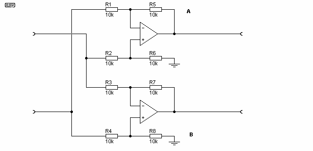
Figure 5 - Balancing Differential Preamplifier
Alternatively, if you have an unbalanced source, you may simplify the design by just inverting the input signal with a single op-amp. Omit RXC and RXOGand you have the circuit Rod has chosen in his project 87 and Analog Devices in the SSM2142 too.
But in both of these alternatives there is a snag: A reverse feedthrough from the outputs to the input(s). Therefore either a low impedance source should be used, or another op-amp connected as a buffer should precede the inverter(s). This will finally lead to 'ultimate perfection'  .
.
Without the latter input improvement, a common mode output resistance RCOut of 5 kΩ, determined by RAG in parallel with RBG, is reasonable, but with resistor tolerances of 1% the asymmetry may become quite high. It is not likely that the amplifier becomes unstable. I prefer to use either 0.1% resistors, or the resistors should be measured out so that RXYI / RXYO is quite equal or the dividers should be trimmed. With multiple of these measures RCOut may easily be risen far above 1 MΩ typically.
With the input improvement, RXC and RXOG should be omitted. By using 1% resistors RCOut in 99% of all cases will become between 7 and 20 kΩ, combined with very good CMRRs. With 0.1% resistors and both RXC = 90 Ω RCOut in 99% of all cases will even become between 70 and 200 kΩ.
But do not forget to trim at least one of the op-amps offset voltages: 1 mV offset voltage will cause 400 mV common mode offset voltage if RCOut is 10 kΩ or even 4 V if RCOut is 100 kΩ (!). In order to reduce the differential offset voltage too, the offset voltages of both op-amps must be trimmed. But this seems to me to be less important.
This project is a small, few-weekend project which does not claim to be theoretically, mathematically or scientifically correct and complete. I may have made errors, I may have overlooked better solutions. I was lucky that Rod gave the hint to do the simulation with SIMetrix Intro - as my PSpice Student was too much limited. With this simulation I learned a lot about this circuit.
Rod cared for the circuit to an extent that I really appreciated very much. He 'pushed' me to have closer looks to what I was actually doing, to make simulations and lots of things that finally resulted in the current state. Without him it all would look much more amateurish. Rod, I really have to thank you. You are a great editor!
Main Index
Articles Index