
|
|
| Elliott Sound Products | Project 87 |
 Please Note: PCBs are no longer available for this project, and both are replaced by Project 176. Click the image for the pricelist.
This is essentially an update to the original article on the subject, and includes some ideas to stimulate further thought on the subject. This is especially true of the last section (Hey! That's Cheating) - everyone wants balanced outputs free, well you can have them free (well, near enough anyway).
The balanced transmitter and receiver described in Project 51 work very well, but both are less than optimum under difficult conditions. Uwe has written an article (published on The Audio Pages) describing an active balanced transmitter that has performance almost equivalent to a transformer. There are ICs available that (almost) manage the same thing, and the principle uses feedback to equalise the levels from each transmitter opamp.
While Uwe has gone to a great deal of trouble to get his circuit to match a transformer as well as possible, this is not an easy circuit to get working well, and it requires 0.1% tolerance resistors and wide bandwidth opamps.
Enter ESP and the 'simplification methodology' that I tend to use wherever I can. The result is a transmitter (in particular) that is extremely good, and matches the performance of a transformer to a quite acceptable degree. It's not perfect, but it's stable, and requires no adjustments or close tolerance parts (1% resistors will provide a maximum error of 1/100, or 40dB common mode rejection and balance).
Use of closer tolerance resistors - and good or premium opamps - will give a circuit with excellent performance, and it will come very close to that of a transformer balanced circuit with none of the associated cost. Response is flat to at least 50kHz, with a low frequency limit of DC (as shown). Capacitors can be used to limit the low frequency limit if desired.
The receiver is shown in Figure 1, and as shown does not have any RF protection. This configuration is somewhat better behaved than that shown in the original article, and presents exactly the same impedance to each of the balanced lines in the cable. This is also the case with the original version shown, but only if the source is also balanced.
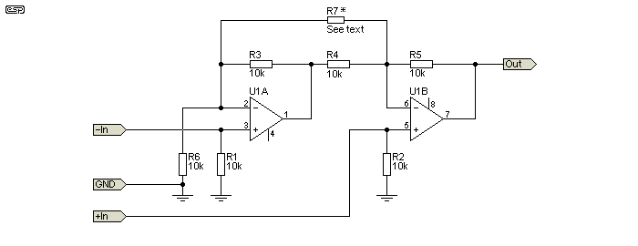
The resistor marked * (R7) may be left out, and the circuit will have a gain of 2. Installing this resistor will increase gain, but will have no effect on the input impedances or balance performance. The minimum gain for this circuit is 1.5 (if R6 and R7 are omitted), and this increases to 2 with R6 installed. The gain setting resistor R7 still works if R6 is omitted, with a value of 10k providing a gain of 3.5, and 1k giving a gain of 21 (26dB).
 | The standard pinouts for a dual opamp are shown (top view of device). You should always use a bypass capacitor (typically a 100nF ceramic or polyester) connected between pins 4 and 8, as close to each opamp package as possible. Even with 'slow' opamps, it is always a good idea to use a bypass cap to prevent possible instability at high frequencies. With all circuits shown, dual opamps are indicated. Pin 4 is negative, pin 8 is positive. The supply voltage should be between ±9V and ±15V, although some opamps may be satisfactory with supply voltages down to ±5V. |
The exact same scheme as shown in the original project could be used for the inputs on this version. One possible connection is shown in Figure 2. This is virtually identical to the configuration shown in Project 51, and will provide a very high noise rejection. Feel free to reduce the resistor values for lower noise, with a corresponding increase in the capacitor value. For example, if the resistance is reduced to 1k, the capacitance should be 1.5nF for the same -3dB frequency (a bit over 100kHz).

The 10k resistors (R1 and R2) to ground are still needed, and this arrangement will reduce the gain by a little over 7db. Use lower value resistors for less attenuation, but remember that as the attenuation is reduced, so is noise immunity. 1k resistors would be the lowest value I'd recommend, and will cause minimum attenuation (about 1.6dB). C1 may be increased if desired, but if too high may cause rolloff of the signal source.
This line driver is quite a bit more complex than the Project 51 version, but this is the price one pays for higher performance. The input is unbalanced, and has an input impedance of 11k. This must be driven from a low impedance source (such as an opamp's output) or performance will be degraded.
With the values shown, the circuit has a gain of 6dB when measured from the input, and between +Out and -Out. R13 and R14 are not absolutely essential in this version, but are recommended. They enforce a balance on the circuit, and prevent the possibility of 'latch-up' where the outputs get stuck to a supply rail. This is extremely unlikely with the values shown, but the precaution is worth the very minor effort.
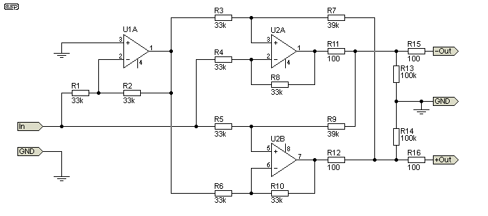
If either output is shorted to ground by connection to an unbalanced input, the output voltage is only 0.4dB less than when operating in fully balanced mode. When one output is shorted, the feedback path to the other opamp is removed, so it provides (almost) the full swing that would normally be available between both opamps. This is the way a transformer (without centre tap) works, so the behaviour of this design is much closer to that of a transformer than the 'standard' balanced output circuit.
It's worth noting that I have seen the schematic of a version of the circuit in Figure 3 (used in a commercial product) that did not include the input inverter. This causes the output to have a significant common mode (in phase) signal at the outputs, and basically it ruins the performance. I have no idea why anyone thought they could get away with the simplification, nor how it was missed during testing. The input inverter (U1A) is essential, or the circuit is worse than useless ... quite literally in fact.
1 Apr 2002 - I tested the circuit shown using 1458 dual opamps and 5% resistors. If the circuit is reliable and shows no bad habits with very basic opamps (basically dual 741s) and ordinary carbon resistors then I know that it will work when you use better components (however, see note below). Indeed, my test version is both stable and surprisingly accurate, despite the lowly parts used to test the circuit's operation. Because the crossed feedback paths are reduced from the optimum (by virtue of making R7 and R9 1.2 times the 'correct' value, i.e. 39k rather than 33k), the overall stability and frequency response is much less dependent on the component values and opamp quality. I was able to verify that even using 741 type opamps, frequency response is less than 1dB down at 75kHz.
 | Although the above circuit does work exactly as described, in general it cannot be recommended for normal use. With high speed opamps,
the circuit can (and likely will) oscillate, especially if there is a capacitive load (such as a cable) connected to the outputs. While it has been used commercially, the results have often
been less than successful, and few commercial products use the scheme. As noted above, at least one commercial offering left out part of the circuit, rendering it useless at best. While it is a very interesting arrangement, it actually fails to emulate a transformer anywhere near as well as might be imagined. The PCB version of the balanced line driver does not use this scheme, for the simple reason that stability cannot be assured. In addition, the impedance balance is sensitive to component tolerance, and impedance balance is far more important than signal balance. |
So, if this 'idealised' circuit is so good (at least in theory), why isn't is used more widely? The secret word here is 'theory'. While the circuit is certainly fairly well behaved (as confirmed by my tests), it's relatively complex, but still fails to provide galvanic isolation. Its only real advantage is that the signal level doesn't change if it's plugged into an unbalanced input, but this is of minimal real benefit. Any level difference is easily corrected with the mixer's gain preset. If the output impedance were effectively infinite to one or the other output (with respect to ground) it would emulate a transformer, but that's not the case.
Consequently, you have a significant number of precision resistors that don't really make a circuit that emulates a transformer properly anyway. This means that the main reason that you'd build the circuit is irrelevant, so there is little reason to persist. If you need galvanic isolation, you need a transformer, and there's no way around it. Consequently, the P87B (shown next) is the 'traditional' circuit arrangement.
For all of this, it's worth building it if you are interested in line driver circuits in general. You will learn how everything interacts, and it's quite good fun to play around with. As for using it in a 'real' circuit there are caveats that make it less than ideal, in particular its sensitivity to capacitive loading (as provided by all cables). Ultimately, if you really need a truly floating balanced output, a transformer is still by far the best option. It also provides galvanic isolation, something that you don't get with any transformerless line driver.
The circuit diagram for the original PCB version (no longer available) is shown below. There is no attempt to emulate a transformer, because the circuit shown in Figure 3 is simply not stable enough with typical cables (which represent a capacitive load) and is too complex for general purpose use. Note that the original PCB has been replaced by Project 176 (Fully Differential Amplifier).
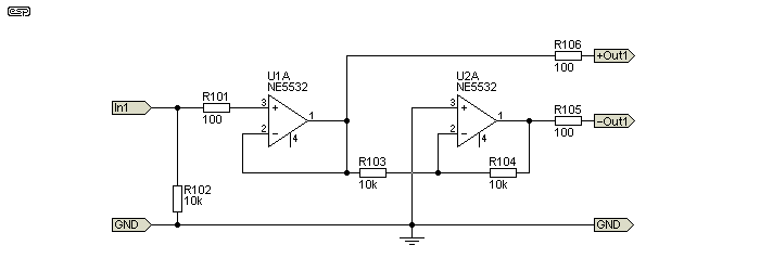
As you can see, this is much more straightforward than the 'idealised' version shown in Figure 3. Only one channel is shown, and the other uses the second half of each dual opamp. While this may be seen as a fairly serious compromise, it's in line with almost all commercial products that offer a balanced line output. It also has the advantage that it is ideal to use as a power amplifier bridging adapter.
Both the transmitter and receiver circuits require at least 1% tolerance resistors, or common mode rejection will be unacceptable. Even with 1% tolerance, the worst case rejection is only 40dB, and if you can use your multimeter to match the resistors to closer tolerance this will improve the performance.
Although the transmitter and receiver are shown with (mainly) 33k and 10k resistors respectively, these may be changed if desired. Any value between 10k and 100k could be used, but remember that higher value resistors create more thermal noise. R7 and R9 in the Figure 3 transmitter are approximately 1.2 times the other resistors - the next E12 value up. For example, if you elected to use 22k resistors throughout, then R7 and R9 would be 27k. Also remember that for the transmitter's input, the impedance is 1/3 of the resistor value used - 10k resistors would therefore give an input impedance of about 3k.
The Figure 3A transmitter has an input impedance of 10k as shown (R102), but this can be increased as required.
Both circuits require a balanced ±12V or ±15V supply (Project 05 or similar power supply), and it must be free of noise. Some opamps will be happy with lower voltages, so check the datasheet. Make sure that 100nF ceramic caps are placed between the supplies as close as possible to the supply pins of the opamps. This is especially important if you use high speed opamps.
Naturally I recommend that you use the PCBs that I have available - Project 176 (Fully Differential Amplifier) - see the ESP price list). These are fully tested, have been built successfully by many constructors and perform exactly as described. The same PCB is used for a line driver or receiver, it's just wired slightly differently (externally).
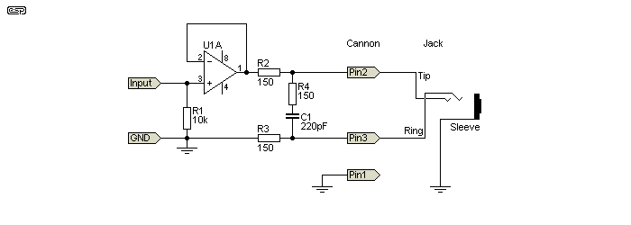
Finally, for those who want a balanced output that is really simple, try the circuit shown in Figure 4. Now look at it again - it's not balanced at all ... or is it?
Now, before you get all horrified, let's have a proper look at what is happening. The main trick with a balanced circuit is that the receiver should 'see' the same impedance on each input. It doesn't actually care that much if there is signal on either or both wires (indeed, that is merely an expectation on our part), but even if the wanted signal is only on one wire, any induced noise will still be common mode, and will still be in phase across both wires. The noise gets cancelled either way, and the signal gets amplified, which is just what we want.
Yes, it's cheating - but it works. Apparently, this trick is used on some of the popular stage mixers, as well as some very well regarded phantom feed microphones (although as far as I know they don't use the Zobel network - this is optional BTW). There is less signal than one would expect (most balanced transmitter circuits have an effective gain of 6dB), but this is generally not an issue. In the case of a microphone, the signal is the same as it would normally be anyway, and with a line output, 6dB of additional gain is usually not a problem to achieve. The amplifier as shown in Figure 4 only needs 2 x 10k resistors in the feedback path to achieve this (10k from output to -ve input (i.e. -in, not -ve supply pin), and 10k from -ve input to ground).
In most cases, this will work just as well as a true balanced output circuit, for the simple reason that it is a true balanced circuit. From the perspective of the balanced input circuit (the receiver), this arrangement provides exactly the same signal quality as if the circuit were fully (signal) balanced, but the signal is -6dB compared to a circuit with a balanced signal. This is rarely a limitation. Although 150 ohm resistors are shown for the balancing network, these can be changed if desired (I suggest a minimum of ~100 ohms though). Normally, I would expect that the values shown will be fine for almost all applications (effective output impedance is 300 ohms).
Somewhat predictably, the signal is only on one lead, so the cables had better be wired correctly if it is feeding an unbalanced input (but this is something that should be regarded as essential for all stage and studio work anyway). The resistors must be of sufficiently high value to ensure that the opamp output impedance is swamped. This ensures that the impedances on each leg are as closely matched as possible.
Caveats - the output impedance of the opamp should be flat to a suitably high frequency, and this will not often be the case with 'cheap and cheerful' devices. I suggest that a high performance opamp should be used to ensure a low output impedance even at the highest frequencies. The optional Zobel network will help ensure that the line appears properly balanced at all frequencies including RF, but cannot guarantee perfect results with any opamp. The venerable NE5534 (or the dual NE5532) is a very good choice, and the LM4562 is even better. These opamps are popular for a very good reason - they have excellent performance. Resistor tolerances are just as important here as with any of the more complex versions - 1% is the minimum acceptable tolerance.
With all balanced interfaces, the impedance balance is the thing that counts. There is not (and never was) any requirement for the signal to be balanced. It doesn't matter if the signal levels are the same or radically different (including having one line with no signal at all). In contrast, an impedance mismatch of only a few ohms is enough to reduce the common mode rejection quite dramatically.
This new project article was inspired by Uwe Beis, and his article on the (almost) perfect balanced transmitter is published on these pages. Although the material here is somewhat 'off topic' from his approach, the inspiration to experiment and try the various techniques came from his submission. I recommend that you read the full article, as it explains the operation of the balanced transmitter shown in Figure 3 very well, and will give you an idea of the dedication of some people (Uwe in this case) to the advancement of their understanding of analogue electronics.
 Main Index
Projects Index Main Index
Projects Index |