

|
| Elliott Sound Products | Project 201 |
 Main Index Main Index
 Projects Index Projects Index
|
This project is based on the MOSFET relay shown in Project 198 and is suitable for use in the Project 62 'LX-800' dimmer, or used as a stand-alone system using 0-10V control, or digitally, using a DAC output to provide 0-10V, or by direct control. In the latter case, the microcontroller will require a zero crossing reference, and the micro will control all timing and switching via the Si8752 couplers.
While the circuit is capable of being used as a leading-edge or trailing-edge dimmer, but trailing edge is the preferred option. Although the Si8751/2 ICs have a fairly fast turn-off time, the turn-on time is slower. As shown in the waveforms shown in Figures 7 and 8, the performance is still acceptable for leading-edge control, but the maximum load should ideally be kept below 100W to keep instantaneous MOSFET dissipation within the safe operating area. Higher power is certainly possible, but you may find that it's too hard to keep the MOSFETs at an acceptable temperature without a fairly substantial heatsink. This is something that needs to be addressed by the constructor, as I can't test all the possibilities.
WARNING: Under no circumstances should any reader construct any mains operated equipment unless absolutely sure of his/her abilities in this area. The author (ESP) takes no responsibility for any injury or death resulting, directly or indirectly, from your inability to appreciate the hazards of household mains voltages. The circuit diagrams have been drawn as accurately as possible, but are offered with no warranty whatsoever. There is also no guarantee that this design meets the regulations which may be in force in your country.
Dimming Basics
Remotely controlled light dimmers in theatrical and show-lighting applications often use an industry-standard 0-10V control signal for controlling the lamp brightness. This is just as applicable to a home system, for which this circuit is designed. The dimmer described here is a trailing edge type, and the while the turn-on time is somewhat leisurely, turn-off time is quite short. This can lead to significant EMI (electro-magnetic interference) unless filters are used on the outputs. Although the circuit shows small inductors and a 'snubber' network, they may not be sufficient to prevent interference with audio systems or even wireless microphones. The 0-10V dimming protocol uses the following relationship ...
0V = lamp off, and
10V = fully on.
Any voltage level between these two values represents a proportional lighting level voltage between those values adjusts the average voltage which is applied to the light bulb. The voltage level from the controller is compared to a ramp signal generated in sync with the mains frequency (50Hz, or 60Hz in US and some other countries).
The lamp circuit is switched on when the levels of the control signal and the ramp are equal. For instance, if the control is set to halfway, that equality will occur when the ramp signal reaches 50% of its level, switching the MOSFETs off. When the mains cycle falls to zero, the MOSFETs are turned on because the ramp signal is pulled to zero volts. Consequently, only half the mains cycle is passed to the lamp by the MOSFETs, and the lamp is at half brightness.
Note that this is not intended to drive high power incandescent lamps as used for stage lighting. It's a low power dimmer (400W maximum at 230V), intended for home lighting. While it's described using pots to set each dimmer, there's no reason that it can't be interfaced with a purpose designed Arduino or similar programmable interface. The only requirement is that the microcontroller can output a 0-5V DC voltage (which may be derived from a PWM output). The 0-5V signal will need to be amplified to 0-10V using LM358 opamps, or you can use a 0-5V ramp signal instead of the 0-10V version shown. This will reduce noise immunity, but if done with care it should be fine. Alternatively, the microcontroller can control the Si8751/2 couplers directly, but it will then require a zero-crossing detector. The detector shown in Figure 2 can be adapted to provide the zero-crossing signal for the micro.
This project was created as an addendum to Project 62, a multi-channel modular dimmer for stage use. The original project was contributed, but this version only became possible with the availability of the Si8752 MOSFET driver IC. The earlier MOSFET dimmer published on the ESP website (Project 157) used a resistively coupled power supply to drive the MOSFET gates and timing circuit, but the Si8752 makes multiple channels easy to achieve. This is irksome (at best) when a separate supply is needed for each dimming circuit.
The phase control system is almost universally used for AC light dimming. The major difference with this design is that unlike 99% of commercial dimmers, it uses MOSFETs to switch the AC rather than SCRs (silicon controlled rectifiers, aka thyristors) or TRIACs. While this is not as cheap to implement, it's a much kinder waveform for electronic loads, such as dimmable LED lighting products. These are now the preferred option for most home lighting, because they are very energy-efficient, long lasting, and have low heat generation (compared to incandescent lamps and most compact fluorescent lamps).
The trailing edge design generates less noise than SCRs or TRIACs, but that does not mean it is noise free. Proper filtering can reduce the noise to acceptable levels, and 'lighting buzz' can be kept to a minimum with proper cabling. The use of mains line filters helps to keep both conducted and radiated emissions to a minimum.
The diagram below shows the load waveform for three different triggering times (after the zero crossing). The first (in red) was triggered 1ms after the zero crossing, the second (green) at 5ms, and the last (blue) at 8ms. As the delay is increased, the available power is reduced. The ramp generator in the next section allows the dimmer module to be triggered anywhere between immediately after the zero crossing (full power) down to just before the next zero crossing (minimum power). If you use the -Ramp signal (see below), it's inverted, and the circuit performs as a leading edge dimmer.
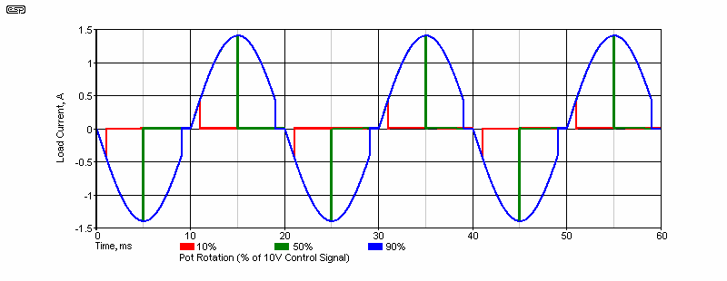
Because the mains waveform is sinusoidal, the power is not linear with decreasing phase angle. The table below shows the relative power levels, using 1ms delay (18° of the half cycle) increments. A delay of 10ms means that the MOSFETs don't turn off, although they actually will for a very short period near the zero crossing point. The loss is negligible. The relationships shown apply to both leading and trailing edge dimmers. The table shows one half-cycle of a 50Hz mains waveform. There is no need to show 360° because the waveform and switching are symmetrical.
| Delay (ms) 50Hz | Delay (ms) 60Hz | Phase | Relative Power |
| 10 | 8.333 | 180° | 100% |
| 9 | 7.497 | 162° | 99.8% |
| 8 | 6.664 | 144° | 95.8% |
| 7 | 5.831 | 126° | 86.1% |
| 6 | 4.998 | 108° | 70.5% |
| 5 | 4.165 | 90° | 51.1% |
| 4 | 3.332 | 72° | 31.6% |
| 3 | 2.499 | 54° | 15.6% |
| 2 | 1.666 | 36° | 5.23% |
| 1 | 0.833 | 18° | 0.75% |
| 0 | 0 | 0° | 0.00% |
Note that the phase angle works for 50Hz and 60Hz equally, but the delay (in milliseconds) is different. For 60Hz, you need to increment the delay by 0.833ms as shown in the '60Hz' column. The same relationships exist for a leading edge dimmer, but the delay figures are reversed because the AC remains off until the delay time has been reached. Any delay caused by the MOSFET relay switching times is insignificant provided it's less than 18° (1ms at 50Hz, or 833µs at 60Hz). Also, note that the power loss is only tiny if the circuit can't achieve a full half-cycle, with 162° only losing 0.2%. In most systems, more than that will be dissipated in the switching circuits.
This is where all the DC voltages are derived, and mains synchronisation ensures that the system is able to detect the point where the AC mains waveform passes through zero, either 100 or 120 times per second. Note that throughout this project, the opamps are all LM358 types. These are low power opamps, but they are able to get their outputs to (close to) zero, and the inputs can be operated from zero up to the supply voltage. These devices should not be substituted unless you are sure that the ones you use have equal specifications. While some readers may be suspicious of using opamps as comparators, the circuitry is all low speed, and the opamps work perfectly in this role. Comparator ICs simply add another resistor to each comparator, but don't improve the circuit's performance.
Note that while you can use a 12V switchmode supply instead of the transformer, you then have to provide a zero-crossing detector that's derived from the mains. This isn't especially difficult, but you need a bridge rectifier and current limiting resistors, all of which are at full mains potential. The zero crossing signal is typically produced using an optocoupler (LED input, transistor output) and the transistor replaces Q1 in the ramp generator circuit. This option is not shown, because it adds an extra layer of danger to the final design, which is avoided by using the circuit shown. There are several zero crossing detectors described in the ESP 'Application Notes' page. See AN005.
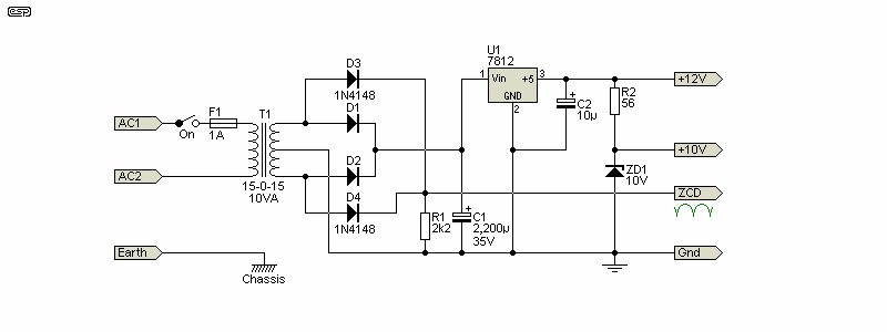
The circuit shows a 15-0-15V 10VA transformer, but a larger one can be used if preferred. The full-wave rectifier can also be replaced by a bridge if used with a single 15V AC winding, and you need the bridge rectifier (for the DC supply) plus two 1N4148 diodes to provide the zero crossing signal. This option isn't shown. Resistors R1 and R2 should be a minimum of 1/2W. Capacitors should be rated at a minimum of 25V, but 35V is better for C1. All diodes (other than zeners or as shown) should be 1N4004 or equivalent. U1 is a standard 12V 3-terminal regulator (LM7812). D3 and D4 (along with R1) are used by the zero crossing detector (ZCD). The ramp generator and other circuitry is shown next. The 10V supply is capable of a maximum of about 20mA. The ramp is created by charging C3 at a constant current, using a current mirror circuit. This was selected because it's insensitive to temperature changes, provided the transistors are in intimate thermal contact.
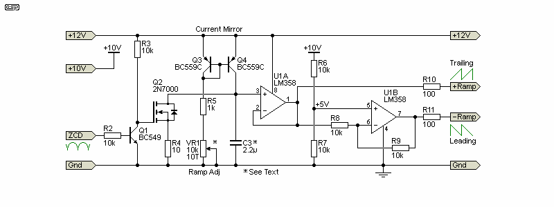
The ramp generator is shown above, and it uses all voltages from the power supply. The ZCD signal turns on Q1, and when the voltage falls to zero, this causes Q1 to turn off, Q2 (2N7000 MOSFET) turns on, discharging the ramp generator capacitor (C3). Q3 and Q4 form the current source that charges C3 linearly, and VR1 is used to set the peak voltage to exactly 10V, as shown below. The ramp signal is buffered by U2A to provide the 'normal' ramp signal, and by U2B to produce an inverted ramp that can be used to convert one or more of the dimmer circuits to leading edge. This will be useful if part of the system is used to drive an inductive load such as iron-core transformers used for halogen down lights.
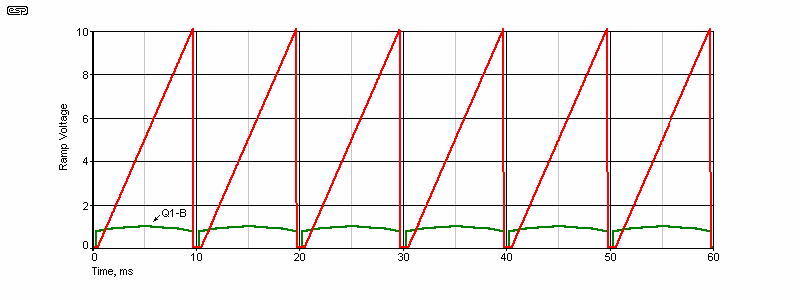
The above shows how a correctly adjusted ramp waveform will appear on an oscilloscope (50 Hz mains signal is shown - ramp frequency is double the mains frequency). The ZCD (zero crossing detector) input waveform is also shown in green, at the base of Q1. The ZCD pulse width is about 550µs. There is no easy way to adjust the circuit without an oscilloscope, but a PC based sampler using the sound card will work fine. You must use an attenuator to make sure that the maximum input voltage of the sound card is not exceeded. If you can't figure out how to do this, then I suggest that you are too inexperienced to attempt this project.
This circuitry produces reliable and accurate synchronisation for the power stages. The circuit generates a 100Hz (or 120Hz for 60Hz countries) ramp signal which is synchronised to the incoming mains voltage. The ramp signal starts at 0V and goes linearly up to 10V in 10 milliseconds (8.33 ms for 60 Hz mains), and repeats with each mains half-cycle. The voltage returns to 0V at each mains voltage zero crossing when C2 is discharged by Q3, a 2N7000 MOSFET. R4 limits the peak current to about 700mA.
The 10k ohm trimpot is used to adjust the ramp so it has exactly 0-10V swing. The 10V level is defined by the actual value of C2, and the current provided by the current mirror (Q3 and Q4) - hence the need for adjustment. Q3 and Q4 must be in close thermal contact (thermal compound and heatshrink tubing to hold them together) to counteract any drift with temperature. Adjusting the trimpot sets the capacitor's charge current, and with a 2.2µF cap as shown the average charge current will be 2.2mA. You must use a polyester or polypropylene cap for C3, as it will be much more stable over time than an electrolytic. Ideally, When the ramp is calibrated using VR1, the dimmer circuits can be left disconnected, as the ramp signal is buffered by U1A (and U1B for the negative ramp).
A 10V input signal (from a fader or other source) turns off the MOSFET at the very end of the waveform, so full brightness is achieved. At zero volts input, the MOSFETs are not turned on at all, so the lamp(s) are off. At intermediate levels, the MOSFETs turn off somewhere between the beginning and end of the waveform - thus at 5V input, the MOSFETs turn off at exactly half way between the AC zero crossing points, so 1/2 the normal sinewave is applied giving about 1/2 brightness - this is not strictly true (as shown in Table 1 above) and because our eyes have a logarithmic response, but it works well enough in practice. The same principle is used for all dimmers, regardless of size or purpose.
The dimmer unit is shown in Figure 10. Each dimmer has an LM358 opamp, which works as a comparator. The output will be high (+10V or thereabouts) when the input signal (0-10V) is greater than the ramp signal. For example, if the console's output voltage is 5V, the output of U1 remains high until the ramp voltage is just below 5V. Once the ramp voltage exceeds the input voltage, the output goes low, and deactivates the Si8752, turning off the MOSFETs. The lamp will receive the first half of each mains half cycle, because the MOSFETs are on for the first half. If this doesn't make sense, refer back to the above section on phase control.
The heart of the circuit is really the Si8752, which is a capacitively coupled MOSFET driver, specifically designed for MOSFET relays. The version used is a 'LED emulator' version, which removes the need for a separate 5V supply and decoupling circuitry. It also (and most importantly) provides essential isolation between the mains and the control circuitry. These devices are rated for 2,500V isolation, and it is imperative that no tracks are run between the pins of the IC, or safety will be seriously compromised. Unfortunately, this IC is only available in a SMD package, so the distance between opposing pins is about 3.8mm - just sufficient to ensure safe creepage and clearance distances.
To convert a dimmer to leading edge, use the '-Ramp' output from the ramp generator instead of the normal '+Ramp'. When the LM358 is active (output high), each Si8752 receives about 14mA drive current. A 4-channel unit will therefore require a maximum supply current of around 60mA. This isn't a great deal of current, so the power supply won't be stressed at all. The current is at the maximum when all outputs are at full power for the both the trailing edge and leading edge versions.
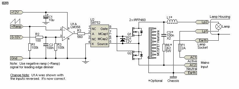
The inductor (L1) and snubber network (C3 and R6) are optional, and will be needed if the dimmer causes any interference. If used, R6 needs to be a wirewound resistor, because instantaneous peak dissipation can be rather high. The MOSFETs must be isolated from the heatsink (to a standard suitable for mains), and the heatsink must be securely bonded to the chassis. This is critical for electrical safety, and all work at this level must be to the highest possible standards. Provided the load is low (less than ~1A for each dimmer), you probably won't need a heatsink, as the dissipation in each MOSFET will be only be about 270mW. The IRFP460 (or SiHFP460) is rated at 500V, 20A, with RDS-on of 0.27Ω. While 1A doesn't sound like much, that's over 200W of LED lighting at 230V (high power factor types). That's a lot of light with LEDs! Even 100W at 120V is a lot of light. Make sure that the fuse is appropriately rated if a heatsink isn't used (not recommended).
Note: If you find that you need faster turn-on, then you'll need to use MOSFETs with either a low gate threshold and/ or devices with the lowest gate capacitance you can find. The STP7NK40ZFP is an example, and it has a threshold voltage of 4.5V, and a gate capacitance of 535pF (typical). It's a relatively low current MOSFET (5.4A) with a 400V rating and zener protected gate. Maximum dissipation is only 70W (at 25°C), and RDS-on is less than 1Ω. There's also a 'full-pack' (fully insulated) version available, but its power dissipation is reduced to 25W due to the high thermal resistance of the built in insulator. Ultimately, it's up to the constructor to choose a MOSFET that meets the requirements of the dimmer. You may think that IGBTs (insulated gate bipolar transistors) could be used, but they are polarity sensitive, and don't have a reverse-parallel diode. They can be used inside a bridge rectifier, but the end result will be larger and far more expensive.
I'd normally expect that this dimmer would be built as a 4-channel unit. The terminal marked '0-10V' is the input from the pots used to control the light level (typically 10k - see Figure 6). With this unit, it is absolutely essential that all mains wiring is fully protected against accidental contact. The MOSFETs may be on a heatsink, and great care is needed to ensure that the unit is completely safe. The insulation between the MOSFET bodies and the heatsink must be 100% reliable with the full mains voltage. Unless you are aiming for more than 3A, a simple flat sheet of aluminium should suffice for the heatsink (for example the case used to house the dimmer(s)). It should not be less than 2mm thick.
Normally, you would use mica (or aluminium oxide) washers, with thermal compound between the MOSFET and mica, and mica to heatsink. However, for this application (and because dissipation is quite low) I suggest silicone pads. Regular readers know that I almost never recommend them, but in this instance it's by far the safest option. The integrity of the insulation is paramount, and the specified MOSFETs have a fully insulated mounting hole to ensure safety. Insulation should be checked with a 1000V insulation tester - any resistance less than infinity on the meter is too low! Remember that heatsink compound must be used with mica, and every care is needed to ensure the final assembly is completely safe. If you use a silicone pad, it must be verified for its insulation capabilities - don't just use whatever you have available!
Alternatively, use fully insulated MOSFETs, which have a full plastic coating across the back of the device, and require no thermal interface material other than thermal grease. These are made by several manufacturers, and the package type is often called 'TO-220F', where the 'F' means 'full-pack' (fully insulated). Some are available for less than AU$2.00 each, assuming that you don't need particularly high power. The 'full pack' will reduce the maximum continuous power by a factor of between 3 and 5 (so a 100W device may be reduced to 25W or less). Always read the datasheet carefully!
Make sure that the MOSFET leads cannot touch the heatsink under any circumstances, including damage, a slipped meter probe or anything else. I suggest that suitable insulating material be placed below the MOSFET leads, preferably screwed to the heatsink. Don't rely on adhesive alone, because it may 'let go' if the heatsink ever gets too hot. This is very unlikely unless the system is overloaded. Remember that the creepage/ clearance distances for a TO220 package (from leads to mounting surface - i.e. heatsink) is only 2mm (2.7mm for TO218 and similar packages). Ensuring safety isn't easy with so little clearance, hence the suggestion to use a silicone pad (preferably oversized).
It's highly unlikely that you'll even consider the use of a fan to cool the MOSFET heatsinks and inductors, but if you do, make sure there is a filter in place so a build-up of dust or other matter can't create a short. If a fan is used, it must blow air onto the parts to be cooled. A fan that sucks air across a heatsink also sucks at keeping it cool!
The case and heatsinks must be earthed via a 3-pin mains plug, and all mains voltage tracks and wiring must be kept a minimum of 5mm from the low voltage circuits. The inductor (L1) needs to be a mains rated interference suppression type. These may be available from electrical installation suppliers, specialist inductor suppliers, or you might have to make your own.
The turn-off time of the MOSFETs (somewhere in the vicinity of 20-50µs) may result in the generation of EMI which can interfere with radio and/or TV reception. This can be reduced by using an EMI filter. The filter shown is an inductor (typically around 10µH) in series with the MOSFETs, and a snubber network (0.1µF X2 type in series with 2.2k wirewound resistor) in parallel. An additional (X2 mains rated) capacitor can also be used directly across the Active and Neutral and/or LP1 and LP2 terminals. The snubber network causes a ring-wave of current through the MOSFETs at turn off time and the filter inductor is selected for resonance at any frequency above the limit of human hearing but below the start of the AM broadcast band for maximum harmonic attenuation.
To make these inductors, try about 10 turns of insulated wire wound on a powdered iron toroid. Do not use a high permeability core such as ferrite or steel, as these will saturate and may damage the MOSFETs. Make sure that the inductors are firmly mounted, and that accidental contact is not possible while the system is live. Larger chokes should not be used, because the flyback voltage generated when the MOSFETs turn off may cause damage. While the IRFP460 devices are rated for pulsed avalanche conditions, it increases dissipation - potentially by a significant margin.

The control section is nothing more than an array of 10k pots, with one for each dimmer. A 4-channel system is assumed, but it can be bigger or smaller. Larger units may require a more robust power supply, as the one shown above has limited current capability. It will handle up to eight channels without changes, but if you need more than that you will need a 'proper' regulator to get the 10V supply, and the 12V supply may also need to be able to supply more current. The ramp buffers should be able to handle up to 20 channels, but the ramp amplitude may require adjustment.
Ideally, the power supply and ramp generator will comprise one module, with each dimmer circuit as a separate entity. This is suggested because if anything is going to go wrong, it will usually be a MOSFET that fails. If possible, arrange for the boards to plug onto the output connectors with spade connectors so that they could be replaced quickly and easily. You are free to build this section to suit yourself, but make sure that you build it so that repairs will be as easy as possible. Also, make sure that all mains wiring regulations for your country are followed to the letter.
Although a 2A fuse is shown on the incoming mains, you can use a circuit breaker if you wish. The breaker should be rated for no more than 10A, and it should be a thermal-magnetic type so that it will trip instantly with a fault condition. Use of a 'delayed' (D-Curve) breaker will allow for short-term overloads without tripping. For example, if all lamps are switched to full power from cold, there will be a fairly high inrush current that can (and should be) accommodated without tripping the breaker.
The master (mains) switch (if desired) is not shown, but the mains input and main fuse are included. Use a circuit breaker if preferred. If you need a schematic to show how they are wired, then you don't know enough about electrical wiring to tackle the job. In this case, it is recommended that you find someone qualified to carefully check your work, and preferably perform all mains wiring for you.
The following waveforms were captured, but using my signal generator to turn the MOSFETs on and off. Because there was a tiny bit of mains frequency drift, I was able to capture a leading-edge and trailing-edge waveform. The supply voltage was about 230V AC, with an incandescent lamp as the load (I keep a few for just this purpose).
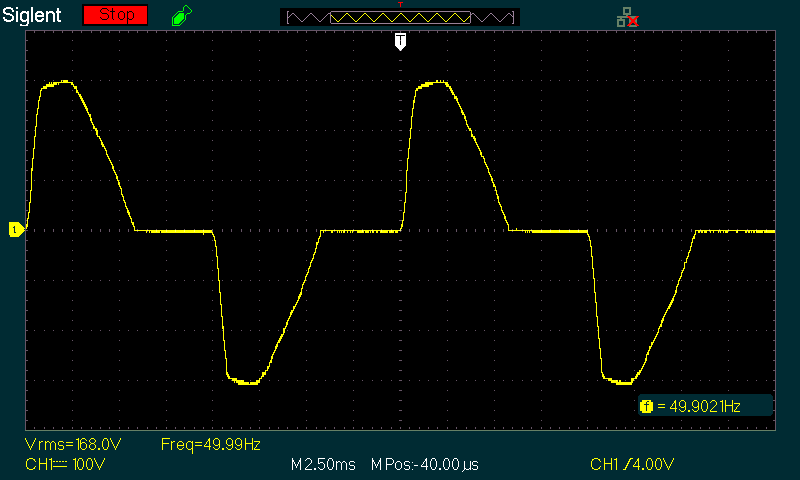
As a leading edge dimmer, the circuit is only just fast enough to keep the MOSFET's instantaneous dissipation to a reasonable figure, but since the primary purpose of the project is as a trailing edge dimmer, this isn't a major limitation. It does mean that you need to be more careful with the peak current, but overall I'd consider the response 'acceptable'. Unlike TRIAC leading edge dimmers, the slow turn-on will keep harmonics low, but it's only suitable for electronic loads (LED lamps) that don't work properly with a trailing edge dimmer (and yes, these do exist - I have some in my dining room). If used in leading edge mode, keep the total power fairly low - perhaps 100W or so would be a reasonable limit. With LED lighting, that's still plenty of light.
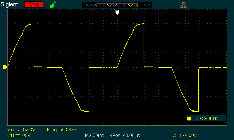
As a trailing edge dimmer, it can't really be faulted in any way. The turn-off time is quite respectable, and turn-on isn't an issue because the AC waveform is fairly slow at the zero crossing anyway, so the relatively slow turn-on time just doesn't matter. As long as it's faster than the mains waveform, there's no issue with it. The MOSFETs I used for this test are STW20NK50Z types, which have a significantly higher gate capacitance (5.2nF for the pair!) than those suggested, so turn-on performance is not as good as it can be. Nevertheless, I'm quite pleased with the results, and it shows that the circuit works as intended.
 Main Index Main Index
 Projects Index Projects Index
|