

|
| Elliott Sound Products | AN-005 |
 Main Index Main Index
 App. Notes Index App. Notes Index
|
Zero crossing detectors as a group are not a well-understood application, although they are essential elements in a wide range of products. It has probably escaped the notice of readers who have looked at the lighting controller or the Linkwitz Cosine Burst Generator (both are on the ESP website), but these rely on a zero crossing detector for their operation. So too does the ESP Tone Burst Generator project.
A zero crossing detector (ZCD) literally detects the transition of a signal waveform from positive to negative (and vice versa), ideally providing a narrow pulse that coincides exactly with the zero voltage condition. At first glance, this would appear to be an easy enough task, but in fact it is quite complex, especially where high frequencies are involved. In this instance, even 1kHz starts to present a real challenge if extreme accuracy is needed.
The not so humble comparator plays a vital role - without it, most precision zero crossing detectors would not work, and we'd be without digital audio, PWM and a multitude of other applications that are perhaps taken for granted.
If you search the Net for zero crossing detectors, you will see a multitude of circuits suggesting the venerable µA741. The circuits will work, but the 741 is several orders of magnitude too slow to be even remotely usable at frequencies above perhaps 100Hz or so. The slew rate of a µA741 is 0.5V/µs - it's one of the slowest opamps around. In all cases, the 741 should be replaced with something considerably faster, such as an uncompensated LM301 or a 'real' comparator. By comparison, a TL071 opamp has a typical unity gain slew rate of 13V/µs, and even that is slow compared to most comparators (note however, this slew rate is not necessarily achieved open-loop). Expect dedicated comparators to have a slew rate of at least 100V/µs!
The reader may also wish to have a look at the zero crossing detector described in the article about Comparators, which includes a circuit that can perform very well with audio frequencies up to at least 10kHz. It's more complex than the ones shown here, but is also a great deal more versatile. It's easy to get a pulse duty cycle of less than 2% at 1kHz. Similar results can be obtained from some of the other circuits described here, provided a fast enough comparator is used.
The ideal zero crossing detector has infinite gain, and will change its output state at the exact moment the input signal passes through zero. The output state change should be instantaneous.
It goes without saying that the 'ideal' does not exist, and there are many factors that influence the end result. All devices have finite gain (typically up to 100dB or so), and that limits the ultimate sensitivity to a change of voltage at the input. The input transistors of a comparator based circuit will never be perfectly matched, so the zero point can be displaced by several (or many) millivolts. All active circuits are subject to speed limitations, and nothing is instant. The output voltage can't change from (say) zero to 5V without some finite speed limit (known as slew rate). There is also the circuit's reaction time (propagation delay) that has to be considered, as that determines how quickly a signal gets from the input to the output. The limitations of real circuits have to be considered during the design process. While reality can be disappointing, that's what we have to live with.
Figure 1 shows the zero crossing detector as used for the dimmer ramp generator in Project 62. This circuit has been around (almost) forever, and it does work reasonably well. Although it has almost zero phase inaccuracy, that is largely because the pulse is so broad that any inaccuracy is completely swamped. The comparator function is handled by transistor Q1 - very basic, but adequate for the job.
The circuit is also sensitive to level, and for acceptable performance the AC waveform needs to be of reasonably high amplitude. 12-15V AC is typical. If the voltage is too low, the pulse width will increase. The arrangement shown actually gives better performance than the version shown in Project 62 and elsewhere on the Net. In case you were wondering, R1 is there to ensure that the voltage falls to zero - stray capacitance and even the tiniest amount of diode leakage current is sufficient to stop the circuit from working without it.
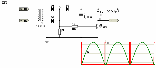
The pulse width of this circuit (at 50Hz) is typically around 600µs (0.6ms) which sounds fast enough. The problem is that at 50Hz each half cycle takes only 10ms (8.33ms at 60Hz), so the pulse width is over 5% of the total period. This is why most dimmers can only claim a range of 10%-90% - the zero crossing pulse lasts too long to allow more range.
While this is not a problem with the average dimmer, it is not acceptable for precision applications. For a tone burst generator (either the cosine burst or a 'conventional' tone burst generator), any inaccuracy will cause the switched waveform to contain glitches. The seriousness of this depends on the application.
Precision zero crossing detectors come in a fairly wide range of topologies, some interesting, others not. One of the most common is shown in Project 58, and is commonly used for this application. The exclusive-OR (XOR) gate makes an excellent edge detector, as shown in Figure 2. The risetime of the input signal is critical - if it's too slow, there will be no output. The total risetime must be less than the delay determined by R1 and C1 (nominally 56ns in the circuit shown).
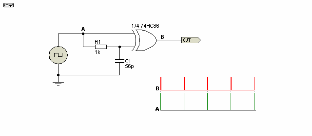
There is no doubt that the circuit shown above is more than capable of excellent results up to quite respectable frequencies. The upper frequency is limited only by the speed of the device used, and a 74HC86 has a propagation delay of only 11ns [ 1 ] and a transition time of 7ns, so operation at 100kHz or above is achievable. The CMOS 4070 can be used, but it has a much greater propagation delay (110ns with a 5V supply) and transition time (100ns with a 5V supply). Timings are 'typical', as shown in datasheets.
The XOR gate is a special case in logic. It will output a '1' only when the inputs are different (i.e. one input must be at logic high (1) and the other at logic low (0V). The resistor and cap form a delay so that when an edge is presented (either rising or falling), the delayed input holds its previous value for a short time. In the example shown, the pulse width is 50ns. The signal is delayed by the propagation time of the device itself (around 11ns), so a small phase error has been introduced. The rise and fall time of the squarewave signal applied was 50ns, and this adds some more phase shift.
Depending on the application, you will need to change the values of R1 and C1. The values shown provide a very narrow pulse (around 50ns), but most circuits don't need to be that fast. The length of the pulse is nominally just the product of the two values (56ns as shown), but that pulse width is too short for some oscilloscopes to display properly. For audio (up to around 10kHz), you can use 10k for R1 and 100pF for C1, giving a pulse width of 1µs.
There is a pattern emerging in this article - the biggest limitation is speed, even for relatively slow signals. Digital logic can operate at very high speeds, and we have well reached the point where the signals can no longer be referred to as '1' and '0' - digital signals are back into the analogue domain, specifically RF technology. PCB tracks become transmission lines, and must often be terminated to prevent serious corruption of the digital waveform.
The next challenge we face is converting the input waveform (we will assume a sinewave or other audio frequency waveform) into sharply defined edges so the XOR can work its magic. Another terribly under-rated building block is the comparator. While opamps can be used for low speed operation (and depending on the application), extreme speed is needed for accurate digitisation of an analogue signal. It may not appear so at first glance, but a zero crossing detector is a special purpose analogue to digital converter (ADC). In some cases, you can use an uncompensated opamp (such as the LM301) as a comparator, but most 'real' comparators are significantly faster. An LM301 was used as a zero crossing detector in Project 143.
The comparator used for a high speed zero crossing detector, a PWM converter or conventional ADC is critical. Low propagation delay and extremely fast operation are not only desirable, they are essential.
Comparators may be the most underrated and under utilised monolithic linear component. This is unfortunate because comparators are one of the most flexible and universally applicable components available. In large measure the lack of recognition is due to the IC opamp, whose versatility allows it to dominate the analog design world. Comparators are frequently perceived as devices that crudely express analog signals in digital form - a 1-bit A/D converter. Strictly speaking, this viewpoint is correct. It is also wastefully constrictive in its outlook. Comparators don't "just compare" in the same way that opamps don't "just amplify". [ 2 ]
The above quote from Linear Technology was so perfect that I just had to include it. Comparators are indeed underrated as a building block, and they have two chief requirements ... low input offset and speed. For the application at hand (a zero crossing detector), both of these factors will determine the final accuracy of the circuit. The XOR has been demonstrated to give a precise and repeatable pulse, but its accuracy depends upon the exact time it 'sees' the transition of the AC waveform across zero. This task belongs to the comparator.
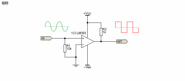
In Figure 3 we see a typical comparator used for this application. The output is a square wave, which is then sent to a circuit such as that in Figure 2. This will create a single pulse for each squarewave transition, and this equates to the zero crossings of the input signal. It is assumed for this application that the input waveform is referenced to zero volts, so swings equally above and below zero. If the input voltage is outside the allowable input voltage of the comparator, it will need to be clamped to ensure the input transistors are not damaged.
Note that most comparators have an open collector output, and the output pin must be connected to a positive supply with a suitable resistor. This is shown in Figure 3, with R2 connected to +Vcc. In most cases, the pull-up resistor (as it's known) can connect to a higher or lower voltage than the comparator's supply, allowing it to act as a level shifter. In some cases, the output can be used to activate a relay, provided the relay current is within the IC's ratings.
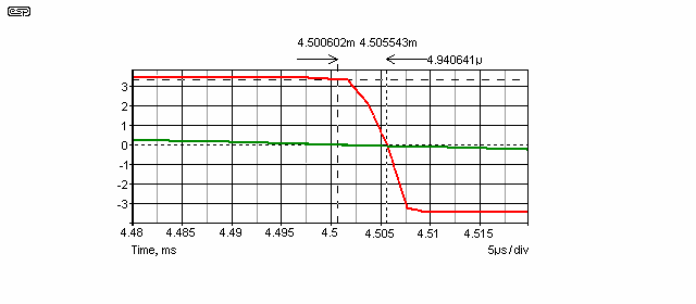
Figure 4 shows how the comparator can mess with our signal, causing the transition to be displaced in time, thereby causing an error. The significance of the error depends entirely on our expectations - there is no point trying to get an error of less than 10ns for a 50/60Hz lamp dimmer, for example.
The LM393 comparator that was used for the simulation is a basic, comparatively low speed type, and with a quoted response time of 300ns it is too slow to be usable in this application. This is made a great deal worse by the propagation delay, which (as simulated) is 1.5µs. In general, the lower the power dissipation of a comparator, the slower it will be, although modern IC techniques have overcome this to some extent. Another choice here would be an LM393, which is very similar.
You can see that the zero crossing of the sinewave (shown in green) occurs well before the output (red) transition - the cursor positions are set for the exact zero crossing of each signal. The output transition starts as the input passes through zero, but because of device delays, the output transition is almost 5µs later. Most of this delay is caused by the rather leisurely pace at which the output changes - in this case, about 5µs for the total 7V peak to peak swing. That gives us a slew rate of 1.4V/µs which is useless for anything above 100Hz or so.
One of the critical factors with the comparator is its supply voltage. Ideally, this should be as low as possible, typically with no more than ±5V. The higher the supply voltage, the further the output voltage has to swing to get from maximum negative to maximum positive and vice versa. While a slew rate of 100V/µs may seem high, that may be too slow for an accurate ADC, pulse width modulator or high frequency zero crossing detector.
At 100V/µs and a total supply voltage of 10V (±5V), it will take 0.1µs (100ns) for the output to swing from one extreme to the other. To get that into the realm of what we need, the slew rate would need to be 1kV/µs, giving a 10ns transition time. Working from Figure 3, you can see that even then there is an additional timing error of 5ns - not large, and in reality probably as good as we can expect.
The problem is that the output doesn't even start to change until the input voltage passes through the reference point (usually ground). If there is any delay caused by slew rate limiting ('transition time') and propagation delay, by the time the output voltage passes through zero volts it is already many nanoseconds late. Extremely high slew rates are possible, and Reference 2 has details of a comparator (LT1016) that is faster than a TTL inverter! Very careful board layout and attention to bypassing is essential at such speeds, or the performance will be worse than woeful.
While zero crossing detectors intended for mains (120V, 60Hz/ 230V, 50Hz) phase control are fairly straightforward, once you are working with higher frequencies (including audio), the requirement for high speed becomes imperative. Naturally, any significant speed increase also means a more expensive part that draws higher current, and much greater care is needed when laying out a PCB than needed for more pedestrian comparators.
This version is contributed by John Rowland [ 3 ] and is a very clever use of an existing IC for a completely new purpose. The DS3486 is a quad RS-422/ RS-423 differential line receiver. Although it only operates from a single 5V supply, the IC can accept an input signal of up to ±25V without damage - however, that's the absolute maximum, and recommended input voltage is ±7V. It is also fairly fast, with a typical quoted propagation time of 19ns and internal hysteresis of 140mV.
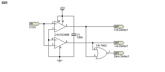
The general scheme is shown in Figure 5. Two of the comparators in the IC are used - one detects when the input voltage is positive and the other detects negative (with respect to earth/ ground). The NOR gate can only produce an output during the brief period when both comparator outputs are low (i.e. close to earth potential).
However, tests show that the two differential receiver channels do not switch at exactly 0.00V. With a typical DS3486 device, the positive detector switches at about 0.015V and the negative detector switches at approximately -0.010V. This results in an asymmetrical dead band of 25mV around 0V. Adding resistors as shown in Figure 6 allows the dead band to be made smaller, and (perhaps more importantly for some applications), it can be made to be symmetrical.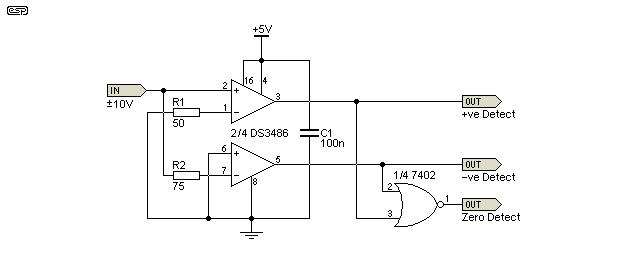
Although fixed resistors are shown, it will generally be necessary to use trimpots. This allows for the variations between individual comparators - even within the same package. This is necessary because the DS3486 is only specified to switch with voltages no greater than ±200mV. The typical voltage is specified to be 70mV (exactly half the hysteresis voltage), but this is not a guaranteed parameter.
Indeed, John Rowland (the original designer of the circuit) told me that only the National Semiconductor devices worked in the circuit - supposedly identical ICs from other manufacturers refused to function. I quote ...
We did some testing with 'equivalent' parts made by other manufacturers, and found very different behavior in the near-zero region. Some parts have lots of hysteresis, some have none, detection thresholds vary from device to device, and in fact even in a quad part like the DS3486 they are different from channel to channel within the same package. Eventually we settled on the National DS3486 with some added resistors on its input pins as shown in Figure 6. The most recent version of the circuit uses trimpots, 100 ohm on the positive detector and 200 ohm on the negative detector. These values allow us to trim almost every DS3486 to balance the noise threshold in the ±5mV to ±15mV range. Occasionally we do get a DS3486 which will not detect in this range. Sometimes, we find that both the positive and negative detectors are tripping on the same side (polarity) of zero, if so we pull that chip and replace it.
The additional resistors allow the detection thresholds to be adjusted to balance the detection region around 0V. The resistor from pin 1 to earth makes the positive detector threshold more positive. The resistor from the input to pin 7 forces the negative detector threshold to become more negative. Typical values are shown for ±25mV detection using National's DS3486 parts. In reality, trimpots are essential to provide in-circuit adjustment.
There are countless ways to make a mains zero crossing detector. In many cases, the simplest circuit will be the most appropriate for a variety of reasons. The most common reason is cost - higher performance circuits need more parts, and that adds not only the cost of the parts, but the PCB real estate needed to accommodate them. When powering anything from the mains, series resistors must be physically larger than their power rating would indicate due to the large voltage gradients across them. Adding more parts simply means that the circuit takes up more space, and that may not be convenient.
The two circuits shown below are examples of simple (but with comparatively high dissipation = wasted power), and more complex, but drawing much lower current from the mains. Many other designs are possible of course, but the two shown should be enough to get you started. There is a balance that needs to be struck between cost, complexity and performance. For example, a high cost precision circuit is not needed for a light dimmer, but a simple, low cost circuit will not have the accuracy required for test instrumentation. Further approaches are shown in the next section.
A zero-crossing detector can be used to detect phase anomalies, or even as a 'loss of AC' detector. If the AC input is interrupted, the output pulse will be much longer than the nominal 1ms, and this is easily picked up by a microcontroller or other circuitry. The Figure 7 or Figure 8 circuit can be used, with the difference being that the output from Figure 7 will simply remain low if the AC fails. Should it remain low for more than 2ms or so, that means that there is no AC.
If your application uses a conventional iron-core transformer power supply, you can use a zero crossing detector as shown in the LX-800 Power Control Section, part of the stage lighting controller that was published back in 2001. While this is a safe and effective option, it can't be used if your circuit relies on a switchmode power supply because the mains waveform isn't available.

| WARNING - The circuits described below involve mains wiring, and in some jurisdictions it may be illegal to work on or build mains powered equipment unless suitably qualified. Electrical safety is critical, and all wiring must be performed to the standards required in your country. ESP will not be held responsible for any loss or damage howsoever caused by the use or misuse of the material provided in this article. If you are not qualified and/or experienced with electrical mains wiring, then you must not attempt to build the circuit described. By continuing and/or building any of the circuits described, you agree that all responsibility for loss, damage (including personal injury or death) is yours alone. Never work on mains equipment while the mains is connected ! | 
|
In the circuits below, there is a line indicated as 'Isolation Barrier'. Everything to the left of the optocoupler (including the LED input pins) is at mains potential, and is waiting to kill you if you're not careful. The section of PCB beneath the optocoupler must not have any copper tracks, and there is an advantage if even the PCB material itself is removed to create an air gap between the 'live' and 'safe' sections. Live wiring should be isolated by an absolute minimum of 5mm from any wiring that is user accessible (connections to potentiometers, input/ output plugs or sockets, etc.).
Mains voltage zero-crossing detectors are common, and are essential with advanced 'phase cut' dimmers and many other mains switching applications. A simple version is shown below, and this was used in the trailing edge dimmer Project 157A and leading edge dimmer Project 157B projects. Resistor dissipation is acceptable (around 400mW in each resistor, 800mW total wasted power), but it's not a precision or low power circuit by any definition. Two resistors are shown to limit the mains current, not because of power, but voltage rating. Ideally they will be 1W types to minimise temperature and provide the maximum voltage rating. Most resistors have a maximum voltage limit that's well below the 325V peak from 230V mains, and using two (or even four) in series limits the voltage across each resistor to a safe value and extends resistor life.
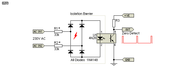
The pulse width depends on the optocoupler, and particularly the transfer ratio (which is based on the LED efficiency and the gain of the transistor). R1 and R2 should be reduced to 15k for 120V operation. It can also be done using an optocoupler with two back-to-back LEDs (e.g. SHF620A, H11AA1 or similar), eliminating the need for a diode bridge. This type of ZCD provides a positive pulse at the zero crossing, which can be converted to negative-going by using the optocoupler's transistor as an emitter follower. (There is no difference in the transfer ratio just because the transistor position is changed.)
As shown, the peak LED current is just under 5mA, but the circuit will work with less. The minimum suggested peak current is around 2.4mA, making R1 and R2 68k. This reduces total dissipation to just under 300mW, but the load on the phototransistor has to be minimised (R3 should not be less than 10k with a 5V supply). This requirement can be relaxed (a little) if the optocoupler has a high current transfer ratio (at least 200%). As the LED ages it will lose output [ 4 ], but maintaining a low forward current keeps this to a minimum. The LED can be expected to last for at least 20 years if the current is kept low (~ 10% of rated maximum is a good starting point).
The 'transfer ratio' (or 'CTR' - current transfer ratio) of optocouplers needs some explanation. If described as '100%' (not uncommon for basic types), that means that 5mA in the LED will allow a maximum transistor current of 5mA. However, this is not a linear function, and the transfer ratio changes depending on LED current, hours of use, transistor collector (or emitter) external resistance and supply voltage. Unless specified for true linear operation, don't imagine that you can use an optocoupler for any signal transfer that requires high linearity. This general class of optocoupler is intended for 'on-off' operation, or for switchmode power supply regulation where linearity is not a requirement.
One disadvantage of the circuit shown above is that the LED in the optocoupler gets current for at least 90% of the time. The zero crossing is indicated by the absence of current as the voltage across the LED falls to zero. Since the LED's useful life is determined by the amount of current it must pass and the total 'on' time, this reduces LED life. By maintaining a relatively low current, the optocoupler should last for a long time, but it's not the optimum way to drive it.
The next circuit was found completely by accident, and because it works so well I asked the designer for permission to publish it here. The detector is very low power, and has particularly good detection of the mains zero crossing point. It's easy to get the pulse down to less than 1ms, and with some component value changes the pulse width can be reduced to around 500µs. While this level of precision isn't needed for most applications, it's inexpensive to implement, and works very well. Note that it will not be operative for a couple of hundred milliseconds after power is applied, because C2 has to charge before the LED current is useful.
The LED gets current only when the input voltage is (close to) zero, so it has a much shorter duty cycle and should therefore last longer. However, the circuit needs an electrolytic capacitor, and these normally have a shorter life than LEDs. However, I don't consider this to be a limitation, because the circuitry on the isolated side will also use electros, and the other benefits of the circuit outweigh that one (very) small negative. The pulse width remains almost constant despite input voltage, with only the slightest change if the mains voltage falls from 230V to 120V. Peak LED current is affected though, and is proportional to the mains input voltage.

The author's page [ 5 ] has a lot of additional information and is recommended reading. R6 is an addition that can be used to reduce the width of the zero-crossing pulse. With the other values as shown, adding R6 reduces the pulse width from 830µs to 440µs, but it also reduces the LED current to about 2mA. R3 is different from the original as well. At 22k (as shown on the author's website), the pulse width is a little over 1ms, but increasing the value provides shorter pulses (and a corresponding increase in precision). The pulse polarity can be reversed by placing the phototransistor's load in the emitter rather than the collector as shown. This is shown in the next drawing.
Because of the high value of the input resistors and the presence of C2 (10µF), the circuit requires some time before it operates normally. It will be fully operational after about 200ms with 230V or 120V mains, but the LED current is reduced with lower mains voltages. For use at 120V, R1 and R2 can be reduced to 100k, which will bring the LED current up to a little over 4mA peak. All diodes are 1N4148 or similar. High voltage diodes are not necessary because the voltage across the diodes is limited by the input resistors, and will not exceed a maximum of perhaps 6-7 volts.
C1 is optional, and can be omitted. It provides a measure of HF noise reduction, but leaving it out is unlikely to cause any issues. Note that as shown, the detector outputs a negative-going as the mains voltage crosses zero. As described above, this can be reversed by using the optocoupler's transistor as an emitter follower. The optocoupler shown in the original circuit is a 4N35, but there are many that can be used. I have a tube of EL817 (4-pin) devices that work well (the LTV817 is an equivalent), but there are countless readily available parts to choose from.
It's worth pointing out that one of the ZCD circuits published on the EDN Network website (and referenced on the DEXTREL site) is wrong in several places, and will not work without corrections. There are also some significant changes that can be made to the EDN circuit, which both simplify the circuit and improve performance. A reader posted a comment to query one error, but no-one ever bothered to reply. I've now included it, and it's actually a good circuit with the changes. It does use more parts than the circuit shown above though. It operates with a significantly higher voltage (across C1) than any of the other circuits, and this is one reason it can produce a ZCD pulse only 150µs wide. Personally, I don't think it's worth any additional complexity, but it may be useful.
The circuit is somewhat sensitive to component value changes. As shown, the voltage across C1 (and Q2) will reach about 45-50V, and this can be reduced by increasing the values of R1 and R2. With 230V mains, you may be able to use up to 330k, but that may not work depending on the transistors. Overall, while it can be made to work well, IMO it's a bit too component-sensitive to be viable. If R1 and R2 are reduced in value it's more predictable, but the voltage across C1 and Q2 can exceed 70V, so higher-voltage parts are necessary.
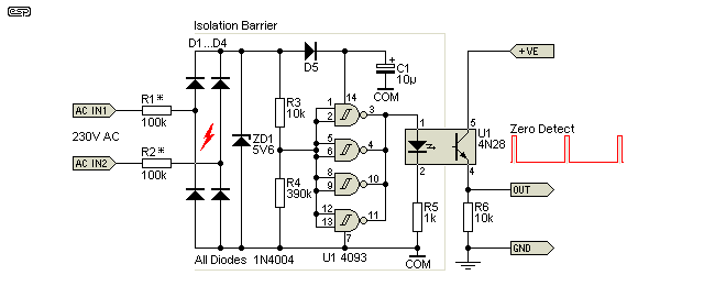
If you think that you need exceptionally high-precision narrow (less than 100µs) zero-crossing pulses, the next two circuits will do just that. The first circuit uses a CMOS 4093 quad Schmitt NAND gate, with all sections wired in parallel. This can achieve a pulse-width of less than 100µs, which is far better than can be achieved with a transistor or two. The input impedance is very high, and using the gates in parallel makes sure they can deliver enough current. The LED in the optocoupler is only pulsed during the zero-crossing. The circuit is fairly immune to noise because of the Schmitt trigger within the IC. You can also use the 74HC132 (also a quad Schmitt NAND gate), but note that it has a different pinout! The 74HC series can provide more output current. The LED current will be about 3mA with the 1k series resistor for the optocoupler, and the value of R5 can be reduced if you need more current.
The next circuit will almost certainly exceed anything that's needed for zero-crossing detection. It's based on an LM393 dual comparator, but only one section is used. It's capable of achieving a pulse width of around 70µs, faster than any other I've seen. It may need some adjustment to the value of R4 if you don't get any output. Reducing R4 increases the pulse width. Again, the LED is pulsed only during the zero-crossing period. Unlike the Fig. 10 circuit, there's no Schmitt trigger and very noisy mains may cause timing problems. I've tested many ZCDs over the years and noise is rarely a problem, contrary to what you might expect.

Current drawn from the mains is minimal (about 2mA RMS). Ideally, you'll use two 27k resistors in series for R1 and R2 to ensure the voltage across each resistor is kept to the minimum. The voltage on U1.2 is about 650mV (set by D6). Because the LM393 comparator can have its inputs at (or even slightly below) ground, the low voltage isn't a problem. The output pulses low when Pin 3 falls below 650mV, and pulls current through the optocoupler's LED. The Fig. 11 circuit is the highest performance ZCD you're likely to find, consistent with physical size and parts count. It's possible to improve it, but there's little reason to do so.
The 10µF filter cap for both circuits looks as if it's far too small, but it can maintain the voltage for the very brief current pulses. Be careful of stray capacitance around the comparator's input pin. If it's more than around 100pF the circuit may not work, and R4 will need to be reduced. Lower values give a wider pulse. The LED current is around 7mA with the 1k series resistor for the optocoupler.
These circuits are included so you can experiment, and they have both been simulated, but the Fig 10 circuit was not tested on the workbench. If this changes this page will be updated with a scope capture. If used with 120V, 60Hz, reduce the value of R1 and R2 (2 x 27k), as only half the resistance is needed, and two resistors in series for each isn't a requirement. The following scope capture was done with an LM358 opamp rather than the LM393 comparator, as I don't have the latter in stock. There are a few circuit changes, but the comparator is better than the LM358. Even so, the very slow LM358 easily managed a pulse-width of only 250µs, perfectly centred on the zero-crossing point of the mains waveform.
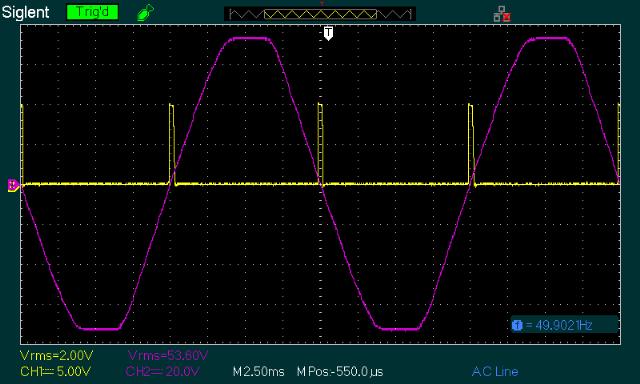
There may be no good reason to use these, as I can't think of an application that needs such a high-precision ZCD pulse. However, if a precision circuit is available, there's no reason to use a 'lesser' version. Both are low cost (although PCB real-estate is greater than the other examples described). Both circuits can be powered from the output of a step-down transformer if this suits your application. R1 and R2 need to be adjusted accordingly.
Both of these circuits are ESP 'originals', and while they use more parts than any of the others, they also have higher performance. One thing that I've found puzzling is the fact that no IC manufacturer has seen fit to offer an integrated ZCD with good performance. The MOC306x and MOC316x zero-cross TRIAC optocouplers demonstrate that it can be done, but they aren't suitable for general-purpose zero-crossing detection.
In May 2022 I became aware of a new IC from Texas Instruments. The AMC23C12 is described as a 'Fast Response, Reinforced Isolated Window Comparator With Adjustable Threshold and Latch Function'. While the datasheet concentrates on power applications (monitoring motor current in particular), it was immediately obvious (to me) that it would make a fine zero-crossing detector. The IC has many different possibilities depending on some specific resistor values (in particular the resistor from the 'Ref' input to 'high-side' ground). There's now another IC - the AMC23C10 (Fast Response, Reinforced Isolated Comparator With Dual Output) which comes with an application note (SBAA542, published March 2022) describing a ZCD.
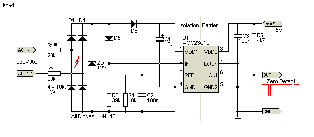
The datasheet claims that both DC inputs need bypass caps (100nF) as close to the IC pins as possible. C1 (10µF) is likely to suffice, but without a unit to test it's not known if this will be enough. At the time of writing, no-one seems to have the ICs available, only evaluation modules that are prohibitively expensive. I've shown the 'Latch' input grounded, but some versions of the IC have dual outputs. If grounded this will not affect operation as the outputs are open-drain (hence R5 pull-up resistor). Note that the ZCD pulse is from 'high' to 'low', the opposite of the other schemes shown.
The IC has very high isolation (7kV DC, 5kV RMS, 1 minute) and is suitable for continuous operation with standard mains voltages. Propagation delay is well below 1µs with the arrangement shown above. There is one characteristic that's a little unfortunate, the 'high-side' current. It's rated for a 'typical' value of 2.9mA with a maximum of 3.6mA, so the input feed resistors have to be a lower value than with the other schemes shown. That means the resistance for 230V should not be less than 40k in total, or 20k for 120V. The resistors should be 1W types to ensure they run cool (the larger surface area results in better heat dissipation).
This final circuit has been included because it's interesting, and shows that other methods of isolation between mains and 'safe' low-voltage circuitry exist. Optocouplers still remain the most common, and this isn't expected to change any time soon. Despite 'lumen depreciation' in LEDs, most optocouplers last for many years.
 Main Index Main Index
 App. Notes Index App. Notes Index
|