

|
| Elliott Sound Products | Project 143 |
Looking on the Net, there is almost a complete absence of tone burst generators or gates, and I confess that I'm puzzled by the lack of information and (more to the point) suitable circuits that can be used to generate tone bursts. There is one other tone burst gate on my site thanks to Siegfried Linkwitz (see Project 58, but that is highly specialised and unfortunately uses parts that are no longer available.
This design is a 'traditional' tone burst generator, and it is intended to be used with an external oscillator. There is no reason that the oscillator can't be included in the same box of course, and I recommend . The gate circuit simply uses a CMOS 4066 analogue switch, but the logic needed makes the project an interesting mix of linear and digital circuitry.
Tone burst testing is useful to measure amplifier overload recovery characteristics, to test loudspeakers at very high instantaneous power levels or to measure the attack and release performance of compressors and limiters. Tone burst testing is also used to check hydrophones and for testing reverberation chambers, spring reverb tanks, etc.
The design shown here is very flexible - far more so than most of the circuits that have ever been published. Back in the late 70s, there were a few designs published, and two of those were the inspiration for this project. One was published by ETI (Electronics Today International) magazine in November 1975, and the other was published by Electronics Australia magazine in March 1979. The latter was intended specifically to test amplifier 'dynamic headroom' based on the (then) standard method recommended by the American Institute of High Fidelity (20ms on-time, at 500ms intervals). I have one of these (built in 1979 or 1980) and it still works, but as published it's not at all flexible. Mine is modified, but on and off times are not adjustable.
These days, most lab work that needs tone burst functions is done with programmable function generators, and the need for a dedicated add-on unit is greatly reduced. It's sometimes possible to find tone burst generators on auction websites, but they are few and far between and not inexpensive. Some are very old and will need servicing before they can be used. This project avoids these pitfalls.
See Part 2 for a few construction hints and a photo of my completed unit.
The schematic for the zero-crossing detector (U1) and gating circuit is shown in Figure 1. The venerable 301 opamp is used for the zero crossing detector because it's extremely fast - it's operated without compensation. Positive feedback is applied via the 10k and 100 ohm resistors, and this provides a small amount of hysteresis to ensure that there are no multiple transitions of the output waveform that goes to the 4024 counter ICs. As noted later in this article, you can use a TL072 for both the zero crossing detector and output buffer. It's nowhere near as fast, but works surprisingly well. (Note that the pinouts for single and dual opamps are completely different!) If you prefer, you can use a high=speed comparator in place of the LM301, which will provide more precise timing. A 1k pullup resistor is required from the output to the positive supply. A further improvement in switching accuracy is obtained if you use the highest input voltage you can, just below clipping (about ±5V or 3.5V RMS).
For this explanatory text, the input signal is assumed to be at 1kHz, so an 'off' delay of 32 cycles represents an off time of 32ms. The timing changes with frequency, because the counters count the number of input cycles, rather than an internal clock signal.
The output pulses from U1 are fed to the clock inputs of the 4024 counter ICs, and a switch is used at each counter to select the number of cycles for on and off periods. As shown, you can have from 1 to 32 cycles on, and from 4 to 64 cycles off. Note that the 'off' count will normally be (much) greater than the 'on' count. This is not a circuit limitation - you can do it if you want, but extremely short 'off' times are not useful.
When the selected counter output ('on' or 'off') goes high, it will apply a brief pulse to the appropriate input of the following NOR gate. Two of these are configured as a set-reset flip-flop (U4A and U4B). The flip-flop output then resets the counter via an inverter, and the cycle continues/repeats. U4A also controls the 'on' gate (U5A), and U4B controls the 'off' gate (U5B). All on and off times follow the standard binary sequence ...
1, 2, 4, 8, 16, 32, 64 ... (and continuing to 128, 256, 512, 1024, 2048, 4096 and 8192 if a second off time counter is added)
The level when the gate is off can be varied from zero (VR1 fully anti-clockwise) up to the maximum (continuous tone). The maximum level can be changed by including R1. As shown (1k) it will limit the maximum level to -1.6dB, but use the value that gives you what you need. In practice (and for the unit I built), it's better to replace R1 with a link, because that allows you to get a continuous tone without having to bypass the tone burst gate.
VR1 is included because when testing a compressor/limiter or power amplifier, you need some signal so the recovery can be seen. VR1 can be replaced with a switch with preset dB ratios is you like, but it's unlikely that you'll need that level of precision - this is a general-purpose test set and makes no claim for being a laboratory standard test instrument. However, there's no reason that it can't be set up to be very accurate indeed.
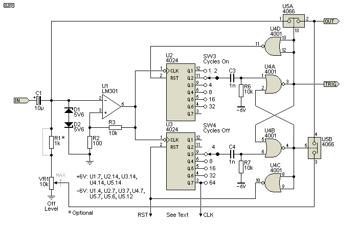
Figure 1 - Zero-Crossing Detector And Tone Gating Circuits
The original circuit showed an alternate single burst trigger, but that has been removed because it doesn't work very well without additional circuitry. If you really want to see how it was done, just click on the image above to see the original version. There was also a drawing error that showed a few points connected to ground that should have been shown connected to -6V. This error has been corrected.
If you decide that you need more than 64 cycles of 'off' time, add a second 4024 for the 'off' counter (connections as shown in the circuit above). The maximum possible 'off' time is roughly 8.2 seconds with the extra counter, based on a 1kHz input signal. It is unlikely that this will be found useful in practice, so most of the extra outputs won't normally be needed. I suggest that anything beyond 1 second is probably not needed. Note that the time is inversely proportional to frequency, so as frequency is increased the time is reduced.
If the 'off' time is (say) 64 cycles, that's 64ms at 1kHz and 6.4ms at 10kHz, or 640ms at 100Hz. With the values shown, the practical upper frequency limit is 10kHz, and although it may extend further this is not guaranteed. It's possible to change values to get a higher frequency, but for most tone-burst testing it's unlikely that you'll ever need or use anything much above 5kHz.
There is also provision for a 'single shot' test mode. SW2 is normally closed, but if opened the output signal will be blocked. Press the 'Burst' switch (SW1) and however many cycles you set via SW3 will be output. Note that there is a delay between pressing SW1 and the output occurring, and that delay is set by the 'off' counter. If set for 32 cycles, there will be a 32ms pause before the output appears. In practice, the single burst requires a very high quality pushbutton with no contact bounce. It can be used with a 'lesser' switch, but will not reliably provide a burst with the number of cycles you selected. Feel free to omit the parts used - C2, R4, R5, SW1 and SW2. Wire U4.11 directly to U2.2 to disable the single burst mode. To obtain a 100% reliable single burst mode requires a more complex switching circuit than the simplified version shown. It does work, but may take a few tries to get a usable result.
The input voltage should be no less than 1V RMS, and no more than 3V RMS. With lower input voltages, the zero-crossing detector will start to introduce significant errors that will cause spikes to occur at the beginning or end of the tone burst. This can be corrected if needs be - see below for more options that you may find useful.
The output impedance of the gate is quite low, but we want to isolate the CMOS gates from the outside world, as well as add an attenuator so the level to the DUT (device under test) can be varied easily. Remember that the input voltage can only be changed over a narrow range before we see problems with the zero-crossing detector, so the level has to be changed after the gating circuits.
The power supply, output amp and sync output isolation (and protection) is shown below. There's nothing special about any of it - the output is just a level control followed by a simple buffer (gain is optional, but not shown). Because the circuit operates on a 12V supply (which must be floating), the maximum output level is around 3V RMS. We can't get more because the supply rails are too low. The incoming 12V DC is 'split' using a resistive divider, to provide the required ±6V supplies. You can increase the incoming DC voltage to a maximum of 15V (±7.5V) - any higher and the CMOS devices will fail!
There's nothing special or even very interesting about the power supply. It's split using a pair of 560 ohm resistors, and there are several capacitors to ensure that the supplies are held at a low impedance. The circuit's current drain is fairly low (not counting the 560 ohm resistors), but it is very important that adequate bypassing is provided for the CMOS chips. While their average current is low, they draw relatively high current as they switch and in extreme cases this can cause false triggering.
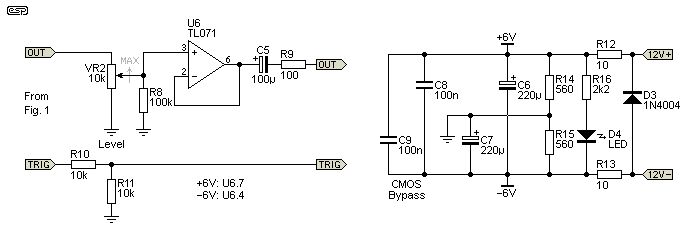
Figure 2 - Output Circuits & Power Supply
The output level control can be replaced with a multi-position switch (or a combination of switch and pot) if desired. The trigger output is intended for use with an oscilloscope - it can be surprisingly difficult to get stable triggering from a tone burst signal. If you use a digital 'scope you can try the single burst option and set the 'scope for a single sweep, triggered by the sudden appearance of the tone burst. Note the comments above regarding the need for a very high quality switch for SW1.
An option that will often be useful is to add the ability to set the trigger level of the zero-crossing detector. This allows you to compensate for input stage DC offset and logic propagation delays. It is quite surprising just how little error is needed to get very audible harshness in the sound of the tone burst. By adding the DC offset control it becomes s simple matter to adjust the offset control until the start and end of the burst is perfect.
I have included a couple of waveforms to show exactly what happens if there is DC offset or propagation delay through the logic circuits. The upper waveform is what the tone burst looks like 'from a distance'. If we zoom in (lower graph, red trace), it's obvious that there's a small error of just under 10mV. This could be caused by a DC offset of about 10mV or a delay of just over 1µs. Should the DC offset or delay become greater, we may see something like the green trace, equivalent to a delay of just under 5µs, equivalent to a DC offset of ~44mV.
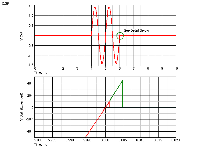
Figure 3 - Burst Waveform Showing Late Triggering
At higher frequencies, the system becomes more sensitive to a delay. 5µs mightn't sound like much, until you have a 10kHz waveform which only takes 100µs to complete a full cycle. If you expect that small errors will cause a problem, use the zero crossing detector shown below. For the most part it's identical to that shown in Figure 1, but adds the DC offset pot that allows you to correct minor errors.
You'll find that if a part of the waveform is cut off, there is little change in the sound of the burst. A spike (either at the beginning or end of the burst) is very audible. If the spike is at the beginning of the burst, that means that the circuit has triggered too early, and the last cycle will have the end cut off. As shown the spike is at the end, indicating that the trigger was late. In this case, the first half-cycle will have a steep rise from zero, because the signal was greater than zero before the gate allowed the signal to pass.
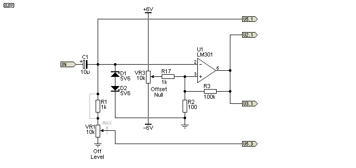
Figure 4 - Zero Crossing Detector With DC Offset Control
The addition isn't complex. The pot (VR3) allows the nominal voltage at pin 3 of U1 to be varied from +600mV to -600mV. The actual voltage range is slightly less because of the positive feedback through R3. The measured average voltage range is ±545mV (based on exact 6V supplies), but it also depends on the opamp to some extent because the peak output voltage swing varies a little from one sample to the next. The range can be reduced by increasing the value of R17 and vice versa. For example, if R17 is 10k, the adjustment range is reduced to approx. ±55mV.
Construction is fairly non-critical, and the circuit can be built on Veroboard or similar. It is highly doubtful that there will ever be enough interest to warrant a PCB, so don't expect one to appear in the pricelist. While it might look complex, I expect that any reasonably competent electronics enthusiast will be able to wire up the board easily enough. I normally never recommend sockets, but for this I consider them essential.
CMOS logic ICs are static sensitive, so it's far better to wire the Veroboard using sockets and plug the ICs in when wiring is complete. You need to cut quite a few Veroboard tracks, so make sure that all cuts fully separate the copper track to prevent shorts that will cause circuit malfunctions. These can be extremely difficult to track down, so be prepared to spend time making sure that you get the circuit right. Note that the piece of Veroboard I used is slightly too narrow, so the connections back to C3 & C4 are right at the edge of the board. Ideally, the Veroboard needs to be at least 2 holes wider, preferably a little more.
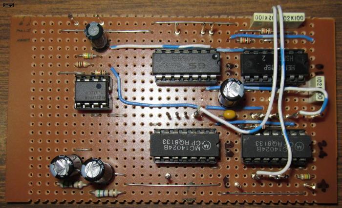
Figure 5 - Construction Suggestion (My Test Board)
The above example shows how I wired the test circuit. As always, with any type of prototype board construction there will be plenty of links. Some will need insulation as shown, others only need to be tinned copper wire. I used pins for all the places where wires connect to switches, inputs and outputs. The mid-air jumpers were added so I could test the circuit, and I used a TL072 for both U1 and U6. It works better than I expected, but as you can see from the oscilloscope capture below, there is a definite need for the DC offset control at low input voltages.
 | Use the pinouts shown here if you decide to use a dual opamp such as a TL072. Most other dual
opamps will also be acceptable, but FET input types are preferred - especially for the minimalist circuit used for the level control. Note that you cannot
use NE5532 opamps, because they have a clamping circuit between the inputs that do not allow them to be used successfully as a comparator. I leave it to the reader to verify that other opamps that might be to hand will function properly. If in doubt, use a TL072 because I know it works. |
If you look very closely, you may notice that some of the resistor values are different from those specified in the schematics. In reality, it doesn't matter much - the analogue part of the circuit is not at all critical. In fact, none of the values are particularly critical, but at least you know that the circuit works with the values I've shown.
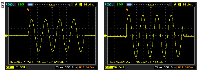
Figure 6 - Oscilloscope Captures From Test Board
The image on the left was taken with a 3V RMS input, which is the absolute maximum. As you can see, it's close to being a perfect tone-burst. When the input voltage is reduced to 100mV, you can see that there is a significant triggering error. The beginning of the waveform is chopped off, and there is a very noticeable spike at the end of the burst. This spike still exists with 3V input, but it's amplitude doesn't change and it's a much smaller proportion of the total voltage (it's about 75mV).
I tested up to 20kHz, and it was still working at even higher frequencies. As noted earlier, I consider the usable maximum frequency to be about 10kHz. If you do plan to use high frequencies, I recommend that you add the extra 4024 counter so you can get a longer 'off' time. At high frequencies, I found that the maximum 64 cycles 'off' wasn't long enough.
Connect to a suitable 12V power supply - remember that it must be floating, with neither side connected to earth/ground. A plug-pack type supply is ideal, and you can use a switchmode type if you don't mind seeing a bit of noise on the output. The filtering shown in Figure 2 will help, but it's very hard to eliminate it completely. The traces shown above were both captured with the test board wired directly to a 12V switchmode supply, but without the resistors. Noise is visible on the 100mV trace, but it's not intrusive (and is inaudible). See Part 2 for a suggestion for the power supply.
The diode shown will help protect the electronics if you inadvertently connect the supply the wrong way around, but will short-circuit the power supply output. Most switchmode supplies have protection circuitry that will prevent failure, but use a polarised plug and socket so that you can't get the wrong polarity. The unit can also be operated with a pair of 6V batteries. 4 x 1.5V cells in series gives 6V, and you need two of them. The two 560 ohm resistors can be omitted, as the zero volt line is set by the batteries. You will need to switch both positive and negative supplies if you use the battery option.
You can use a resistor (100 ohms will do) in series with the supply when you first power-up (assuming a single 12V power supply). This will limit the current if you made an error, but that doesn't mean that the ICs will survive. Fortunately, they are all cheap (except the LM301, which is very old and isn't as cheap as more modern opamps).
 Main Index
 Projects Index