
|
|
| Elliott Sound Products | Project 198 |
![]()
![]() PCBs are available for this project. Click here for details.
PCBs are available for this project. Click here for details.
The concept of MOSFET relays has always been a bit esoteric, but the (relatively) recent introduction of an IC designed specifically for MOSFET relays has changed everything. Before the introduction of the Si8751 and Si8752, the choices were sub-optimal. Photovoltaic optocouplers are available for the purpose, but their turn-on time is so slow that they are pretty much useless for any serious application. To see all of the options, see the ESP article MOSFET Solid State Relays. These two Silicon Labs ICs are only available in an SMD package (which is a pain for a few reasons), but they have changed the design of MOSFET relays forever.

| Note: Please ensure that you can get the ICs before you buy the PCBs. It's come to my attention that the Si8751/ Si8752 chips are unavailable from most outlets, with lead times being somewhat variable, depending on the supplier. You can (of course) buy the PCBs in anticipation of the ICs arriving, but the best estimate I've seen so far is that supply is unlikely to be available until some time in 2023. This is another example of the worldwide chip shortages that have affected many manufacturers and hobbyists alike. |
There are two versions. The Si8751 is a standard logic level (3.3 - 5.0V) device with a 'programming' pin that lets you select the device current to obtain lowest possible power consumption or highest speed. The Si8752 uses an input stage that Silicon Labs calls 'diode emulation', so it behaves like a standard optocoupler. The MOSFET gate voltage is produced by an internal RF (radio frequency) oscillator, and the gate voltage is transferred via an internal capacitive isolation barrier. Unfortunately, there's no 'equivalent circuit' in the datasheet, so some aspects of the design are a little mysterious.
There's no requirement for miniature power supplies on the MOSFET side, and in most cases you probably don't even need to include zener diodes to protect the MOSFET gates from excessive voltages. They are shown in each of the circuits below and indicated as optional. For applications where the MOSFET input voltage is expected to change very quickly, there's provision for 'Miller' capacitors that ensure that the gate voltage cannot rise unexpectedly due to gate-drain capacitance.
As far as I'm aware, this is the only device that can drive the MOSFET gates fully, without requiring a power supply on the secondary side of the isolation barrier. Although there aren't any alternatives, it's inexpensive, and should be available from major suppliers for less than AU$3.00 each, even in small quantities. While this article might appear to be an advertisement for Silicon Labs, I can assure the reader that the ICs I used for testing were paid for, and this article isn't sponsored in any way.

Complete MOSFET Relay Photo
Be aware that for high voltages or high current operation, you cannot use Veroboard or similar. The track spacing doesn't support SMD ICs, and the phenolic backing is not acceptable for high voltages. The tracks are also too thin for high current operation. As noted above, a PCB is available. It's designed to support either version of the IC, and also to be able to be used with most MOSFETs (other than SMD versions which I don't recommend). The MOSFETs shown in the photo are 120V, 70A versions, with very low RDS-on. The PCB will accommodate TO-220 and TO-247 MOSFETs. Please be aware that while it can be used for mains switching, this is not recommended because the creepage and clearances for both the IC and MOSFETs is too close for comfort. However, I've tried it in this role and it works perfectly (but I still don't recommend it unless you know exactly what you're doing).
A brief rundown of some of the equipment classes and applicable standards follows. These are important to understand, as mis-application can result in equipment that is unsafe, with the risks of electric shock, fire or both. The standards applied vary by country, but most use the following definitions and requirements. You must consult the datasheet to see where your design fits into the classifications - it's very detailed and has pretty much everything you need to know.
Class I equipment achieves electric shock protection through basic insulation and protective earth grounding. This requires all conductive parts that could assume a hazardous voltage in the event of basic insulation failure to be connected to a protective earth conductor. Class II equipment provides protection using double or reinforced insulation and hence no ground is required. Class III equipment operates from a SELV (Safety Extra Low Voltage) supply circuit, which means it inherently protects against electric shock, as it is impossible for hazardous voltages to be generated within the equipment.
Understanding the standard and the above classes of equipment requires a clear understanding of the circuit definitions, types of insulation and other terminology used in relation to power supplies.
| Voltage Rating | Description |
| Hazardous Voltage | Any voltage exceeding 42.2V AC peak or 60V DC without a limited current circuit. |
| Extra-Low Voltage (ELV) | A voltage in a secondary circuit not exceeding 42.4V AC peak or 60V DC, the circuit being separated from hazardous voltage by at least basic insulation. |
| Safety Extra-Low Voltage (SELV) Circuit | A secondary circuit that cannot reach a hazardous voltage between any two accessible parts or an accessible part and protective earth under normal operation or while experiencing
a single fault. In the event of a single fault condition (insulation or component failure) the voltage in accessible parts of SELV circuits shall not exceed 42.4V AC peak or 60V DC for
longer than 200ms. An absolute limit of 71V AC peak or 120V DC must not be exceeded. SELV circuits must be separated from hazardous voltages, e.g. primary circuits, by two levels of protection, which may be double insulation, or basic insulation combined with an earthed conductive barrier. SELV secondaries are considered safe for operator access. Circuits fed by SELV power supply outputs do not require extensive safety testing or creepage and clearance evaluations. |
| Limited Current Circuits | These circuits may be accessible even though voltages are in excess of SELV requirements. A limited current circuit is designed to ensure that under a fault condition, the current that
can be drawn is not hazardous. Limits are detailed as follows:
|
There are several MOSFET relays available as ICs, but finding one intended for high voltage or high current is another matter altogether. While they do exist, they are generally expensive and are almost impossible to buy anywhere. The article MOSFET Relays shows some of the options available, but none is really suitable for mains switching, because it's too hard to ensure that the safety barrier is rated for the full mains voltage.
The design shown here is suited for AC or DC, and the voltage and current ratings are determined by the MOSFETs used. Turn-on and turn-off time are typically both under 100µs, making it faster than any electromechanical relay. While the circuit can be used with inductive loads, you have to be careful to avoid high back-EMF from the load, or use MOSFETs that are rated for controlled avalanche conditions sufficient to ensure they will survive.
Note: A complete rundown of inductive loads, including tests with a speaker and a vicious test using a 2mH inductor that forces MOSFETs into avalanche breakdown is now available. See Project 255, another MOSFET relay project that uses commonly available parts throughout. It's probably not what you expect, but I performed many tests I fully expected to be destructive, without a failure. The link takes you directly to the section on back-EMF.
The relay can be used with mains, high power audio (as a loudspeaker protection relay) or DC - it depends on how it's wired. This may not be a cheap project depending on the voltage and current, but the few parts (excluding the IC and MOSFETs) are standard cheap components that you can buy anywhere. If you budget around AU$10.00 or so for the two MOSFETs, it's likely to cost no more than AU$15.00 for parts, but what you get is pretty much unavailable from any supplier.
The overall design is superficially simple, but the reality is very different. The biggest hurdle is ensuring that there is adequate isolation between the control side (low voltage, 'safe') and the switching side (high voltage, hazardous voltage). The drawings show an 'Input' and 'Output' terminal, but these are fully interchangeable. The load is connected in series with the MOSFET relay, and it makes no difference if it's on the 'Input' or 'Output' side.
There are some miniature power supplies intended specifically for powering IGBTs (insulated gate bipolar transistors), and one of these could be used along with an optocoupler to provide full isolation of mains voltage from the low voltage control circuitry. The problem will be actually getting them, as there's not a great call for them for anyone other than major manufacturers. Suppliers who service the DIY market are unlikely to have anything suitable. Those in some countries will have no problems, but elsewhere ... ?
Part of the design goal is to have the control side able to be operated from no more than 12V, and preferably at low current so it makes no demands on existing power supplies. It also has to be small enough to allow everything to fit on a single (small) PCB to make a complete system. There are multiple conflicting requirements, as always.
Other aspects of the design are dictated by the end usage. There are many possibilities, ranging from a loudspeaker protection system that has no difficulty breaking a high DC potential with no arc, through to mains voltage control where the mains can be turned on or off at a specific point on the AC waveform. The latter requires a zero crossing detector, which will be a separate circuit - there are no plans to include zero crossing detection in the current design.
Two very important parameters are creepage and clearance distances. Creepage is the distance across a surface (e.g. IC body or PCB), and clearance is the distance through the air that separates the low voltage from the high voltage side. Because the IC is surface mount, the maximum distance is about 3.8mm, which is sufficient for Class I (basic insulation equipment using a protective earth). Class II (double insulated/ reinforced insulation generally demands larger creepage and clearance distances, so if this project is used for mains applications the equipment must be connected using a 3-pin mains plug with protective earth. The datasheet provides regulatory information for UL, VDE, CSA and CQC. Overall, I do not recommend that it be used in Class II equipment if used to switch mains voltage.
The choice of suitable MOSFETs is huge - so much so that I'll only attempt a couple of types for consideration. A popular and inexpensive part is the IRF540N. It's rated at 33A with a voltage rating of 100V, so it can be used with supply voltages up to about ±70V. Another worth considering is the IRFP460, 550V and 20A. RDS (on) is 0.27Ω, higher than desirable, but 2 or more can be paralleled to reduce it if needed. There are many others, and I leave it to the reader to find a device that suits the purpose and the budget. The total series resistance will be double the RDS (on) of each MOSFET. At any load current there will be a loss that can be calculated using standard power calculations. For example, at 5A peak with 0.5 ohms total 'on' resistance, the peak loss is 12.5W (6.25W each), with an average of about 3.2W for each MOSFET.
Ultimately, the choice has to be left to the constructor, as there are countless MOSFETs that are available, and the choice depends on the voltage and current being switched.
For specialised applications (high voltage or current etc.) the MOSFET selection depends on the requirements. There are too many for me to even consider here, so this is left to the constructor. If there's a choice between otherwise similar MOSFETs, select those with the lowest gate capacitance for fastest switching. Even though the Si8751/2 drivers are much faster than any photovoltaic optocoupler, they can't provide high current to charge the gate capacitance quickly. Remember that there will generally be two MOSFETs, so the gate capacitance is twice that for a single device.
For example, an IRF540N MOSFET with a total gate charge of 14nC (nano Coulombs) requires a voltage of 10V, so the effective capacitance is 1.4nF, and that's increased to 2.8nF with two MOSFETs. Because of limited current capability, the turn-on time will be fairly slow (but still well under 1ms), so this isn't necessarily a problem if the MOSFETs are able to handle the instantaneous power. Because there are so many possibilities, some degree of experimentation will be necessary to determine the overall performance in the desired application.
Each of the drawings shows a 'Common' connection, but this is not normally used. If you make a relay as shown but want to use it for DC, then the common point can be used, with the 'Input' and 'Output' terminals joined. This means the relay can carry twice the current, with a lower overall 'on' resistance. You can also just use a single MOSFET, with the common terminal used as the input or output, depending on the polarity of the DC. You can also use P-Channel MOSFETs (simply reverse the Gate and Source connections), but there's no advantage in doing so because P-Channel MOSFETs are almost always inferior to N-Channel types.
Although I've not shown any circuits using them, there is no reason that you can't use these driver ICs with IGBTs (insulated gate bipolar transistors). These are available with very high voltage and current ratings, but are not suited to audio applications such as speaker protection relays. There is a wide choice, but they are generally fairly expensive (compared to MOSFETs). However, if you need a peak current rating of well over 200A with a 600V rating, no MOSFET will come close! However, they usually have a fairly high gate capacitance, causing relatively slow turn-on times.
Although it's unlikely to cause any issues in use, the MOSFETs should have a reasonable avalanche breakdown rating. A speaker load is partially inductive (but with a fairly low Q), so there may be some inductive 'kick-back' when the DC fault current is interrupted. The IRF540N has a single-pulse avalanche rating of 185mJ (milli-Joules). A Joule is a watt-second, so that allows for an instantaneous dissipation of 1.85kW for 100μs. This is roughly the back-EMF created by a damped 100mH inductor when 50V DC at 12A is interrupted. If the MOSFET goes into avalanche breakdown for 40μs, the instantaneous power is about 900W (36mJ). This is well within the maximum allowable avalanche rating. Being unwilling to subject a real speaker to a 50V DC fault current, I simulated the back-EMF from a more-or-less typical 2-way speaker, and it's unlikely that the back-EMF transient will last for more than ~1μs. However, this can vary depending on the nature of the crossover network.
If you are concerned and wish to mitigate the avalanche dissipation, consider using an MOV (metal oxide varistor) in parallel with the speaker terminals. The rated operating voltage should be at least 25% greater than the amp's peak output voltage, so for an amp with ±50V supply rails, the MOV should be rated for a minimum of 75V. Alternately, TVS (transient voltage suppressor) diodes are available with varying voltages, and a peak dissipation of more than 1.5kW. At under AU$2.00 or so each, this is a worthwhile investment. Note that the MOSFETs suggested in the construction article are rated for an avalanche energy of 256mJ at up to 72A - they won't blow up!
Although I have shown IRF540N MOSFETs in this project, this is more a matter of convenience than anything else. While these will be suitable for low voltage AC/ DC applications, they are not suited to very high current. The claimed RDS (on) is acceptable (44mΩ for the IRF540N), but there are much better MOSFETs available now, having RDS (on) below 20mΩ. I leave it as an exercise for the reader to select MOSFETs that are suited to the voltage and current available from the amplifier to be switched. There are many to choose from, and it would be rather pointless for me to try to list all those that you may (or may not) be able to get easily where you live. You can use multiple smaller units in parallel, which may work out cheaper. The lower the value of drain-source resistance, the lower the distortion contributed by the circuit.
The schematic of the SSR (solid state relay) is shown in Figure 1. Two N-Channel switching MOSFETs are used, with their sources and gates joined. The signal and load are connected to each of the drain terminals - it doesn't matter which is which, because the 'switch' is symmetrical. However, bear in mind that there are two MOSFETs in series, so the effective RDS (on) is double that for a single device. The voltage needed to drive the gates is obtained from the Si8752 MOSFET driver.
The circuit itself is very straightforward. There is one SMD part (the Si8752), and the remaining are conventional through-hole components. While the circuit looks very simple, that is due largely to the IC. The whole circuit is designed specifically to allow it to be used for switching anything from a loudspeaker (as DC protection) to normal 230V/ 120V AC mains. Complete isolation is provided, so the control side can use a micro-controller or any suitable analogue circuitry. The IC requires no more than 15mA input current when activated.
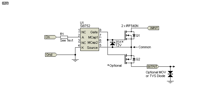
Figure 1 - Si8752 (Diode Emulator) Based MOSFET Driver
With no input current, the MOSFETs are off, so no load current flows. The switching speed (turn-on) is determined by the input current through R1, but it must be less than 30mA. The input can be from any voltage, with the value of R1 selected to provide around 15-20mA. Depending on the MOSFETs used, they will conduct fully when the gate-source voltage exceeds around 7 Volts. It is always a good idea to provide 10-12V gate drive to ensure that they always turn on fully. The zener diode you see is optional, and it's there to protect the delicate insulation between the gate and MOSFET channel. The gate insulation is typically rated for a maximum of around ±20V. Even a little bit of stray capacitance or resistance (moisture on the PCB or a voltage transient for example) can easily allow the voltage to rise to destructive levels because of the very high impedance, and the zener is always a good idea. If drain-gate capacitance is likely to cause problems, the two 'Mcap' inputs can be used. This is covered later.
See the previous section for info on the optional MOV or TVS diode. This may be a good idea if the MOSFETs you use don't have a satisfactory avalanche energy rating. This also applies for the other options shown below.
There are photovoltaic isolators that are designed for this application, but they have very limited voltage and current, and they are extremely slow. Use of big MOSFETs (having a large gate-source capacitance) makes them even slower. Most can't provide more than around 100µA, and voltages of more than 7V require a fairly high drive current. This option is examined in some detail in the MOSFET Relays article, but it's hard to recommend if you need fairly fast on/off switching.
Each MOSFET's voltage should be rated for at least 25% more than the supply voltage to be controlled. This is due to the way the circuit works, and because of the possibility of instantaneous back-EMF from an inductive load when the current is suddenly interrupted. It may be useful to include a MOV (metal oxide varistor) across the SSR switch terminals, or use a resistor/ capacitor 'snubber' to prevent the likelihood of any destructive voltage spike.
To use the relay to its best advantage with a DC supply and load, simply join 'Input' and 'Output' terminals together. These become the +Ve terminal. The 'Common' terminal is then the two MOSFET source connections, which are joined together. The load can be on either side of the relay, because it provides its own gate drive signal via U1 and does not rely on anything on the switched side for gate bias. For a pure DC version there are easier ways to do it though, as it's uncommon to have DC control and load systems separated by isolation. However, this IC does make driving a 'high side' N-Channel MOSFET easy, at least for low frequency applications.
When MOSFETs fail, they almost invariably fail short-circuit (like most semiconductors), and it is essential that these circuits are never used in a safety critical application.
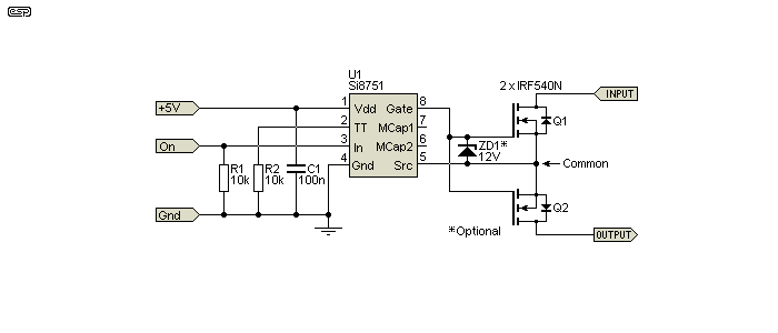
Figure 2 - Si8751 (Logic Level) Based MOSFET Driver
An alternative driver IC is the Si8751. It has performance similar to the Si8752, but it needs a supply voltage (which must be bypassed as shown, and the 'TT' pin programs the current drawn when activated. In turn, this determines how quickly the MOSFETs are turned on. The 'TT' resistor can be bypassed by a capacitor to provide maximum current initially, but with a reduced current once the MOSFETs are turned on. This can reduce power consumption, which may be important in a large circuit with multiple MOSFET relays.
With both circuits, the typical turn-off time is around 15µs (although the spec sheet covers its butt by stating that it may be as high as 35µs). Turn-on time is changed in the Figure 2 circuit by altering the value of R2. If the 'TT' pin is left open, the turn-on time is between 286µs and 650µs, which is generally too slow to be useful. With 10k, it turns on within 58-170µs, and if shorted to ground, that's reduced to 42-120µs. Supply current depends on the value of the resistor (lower values, higher current). The supply current ranges from 1.5mA to 13.8mA, but may reach 17mA in some samples.
It's important that the load's reactive effects be known. Highly inductive or capacitive loads mean that the voltage and current are not in phase, so the relay may need to be derated accordingly. The worst case is a fully reactive load causing a phase shift of 90° (which is unlikely but possible). That means that as the voltage across the relay is at its maximum value, so is the current. That means that MOSFETs rated for 200W, 500V and 20A may only be capable of switching less than 1A before the safe operating area is exceeded. Where there is a chance that fast transitions may occur on the switched signal (including back-EMF from inductive loads), connecting 10pF capacitors to the 'Mcap1' and 'Mcap2' pins ensures that the MOSFETs are held off, even if the gate voltage tries to rise due to drain-gate capacitance. In each drawing, I've included an 'optional' 12V zener diode, which will usually do nothing at all unless there are very rapid transitions in the input (switched) waveform.
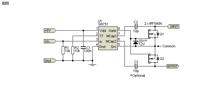
Figure 3 - Si8751 MOSFET Driver With Miller Caps
There are no real issues with reactive loads while the relay is fully on or off, but it's during the switching period that things can go 'pear-shaped' when highly reactive loads are present. Fortunately, the switching time is fairly short, so it's unlikely that most loads will cause a major problem. Care is still necessary with inductive loads in particular to ensure that the SOA (safe operating area) is not exceeded. Ideally, the relay will be turned off as the current passes through zero, so if reactive loads are expected, additional circuitry may be necessary to detect current, and turn off the relay only when the current is close to zero. Mostly, this should not be a major issue, but you do need to be aware of the possible ramifications.
Back-EMF from 'random switched' inductive loads must be considered. When the current is interrupted, the flyback voltage can be very high, and even avalanche rated MOSFETs may be unable to absorb the peak power as the back-EMF is dissipated. Use of zero current switching eliminates this, but it does make the circuit more complex. While a MOSFET relay can be the ideal solution for some applications, that does not mean that the EMR (electromechanical relay) is no longer a viable option. You'd use a MOSFET relay if you need tight control of the on and off time, or for specialty applications such as loudspeaker protection, where the voltage is too high for an EMR (due to contact arcing when trying to interrupt a DC fault current into the speaker).
See the MOSFET Relays article for operation description of the Miller clamp circuitry.
See above section which discusses MOSFET avalanche ratings and the use of MOVs or TVS diodes to suppress transient over-voltage due to inductive back-EMF.
While a MOSFET relay has some significant advantages over and above a traditional electro-mechanical relay, these advantages come at a cost. The MOSFET relay will be physically larger than a conventional relay of similar rated capacity, and the overall circuitry is more complex and costly. Where a relay can be mounted almost anywhere, the MOSFET version requires at least one printed circuit board, as well as more wiring and possibly even a heatsink if it's used at high current. All of this must be protected from accidental contact, because the MOSFET cases may be at mains potential.
Whether it's used as a mains (230V/ 120V) switch or loudspeaker protection relay, a MOSFET relay has advantages that cannot be achieved with electromechanical types, in particular the complete absence of an arc even when switching DC. They are also very fast, and even with no additional circuitry can turn on in less than 100µs, and off in around 20µs. No conventional relay comes close. Unlike TRIAC or SCR based solid state relays, there is little distortion added to the switched signal, and the power dissipated is dependent on the MOSFETs used. With the right devices for the job, dissipation should only be a few watts, and it may be necessary to include a heatsink if the load current is higher than a couple of amps.
Naturally enough, the idea of building your own MOSFET relay should have some appeal, just for the knowledge gained and the experience you'll get, not to mention the fun factor. I leave it to the reader to decide which method to explore and how much fun s/he should have doing so. Please be very careful if switching the mains - it can be deadly if you make a mistake.
 Main Index
Projects Index
Main Index
Projects Index