
|
|
| Elliott Sound Products | Project 255 |
The two existing MOSFET relay projects have been quite popular (Project 198 and Project 245), but both require dedicated MOSFET driver ICs that are not inexpensive and are only available in SMD packages. This isn't necessarily an impediment, but it may make it next to impossible for some constructors if they can't work with SMD parts or can't get the ICs (or both). In addition, there have been supply disruptions (although not recently), and the ICs may become obsolete at some time.
Different PCBs are needed depending on the IC, either the Si8752 or TPSI3052-Q1. The ICs are very different from each other, so a common board was not really possible. It could be done by allowing for both footprints on the board, but that would make it a lot bigger and increase the likelihood of mistakes during construction.
This 'new' version uses mature technology, using a common optocoupler (e.g. LTV817, 4N28 or similar), a general purpose PNP transistor and a couple of resistors. By using a miniature mains transformer with dual secondary windings, two MOSFET relays can be powered completely independently. One thing you do need to verify is the transformer - the isolation voltage between secondaries must be capable of withstanding the total supply voltage without breakdown. If your amplifier runs from ±60V supplies, the two secondaries must be capable of withstanding the full 120V, so they need to be verified to handle at least 500V RMS. I expect that most will be alright, but you do need to check this. Cheap 'no-name' transformers from Asia with no datasheet should be avoided unless you can run a 'hi-pot' (high potential) test yourself, and be confident that your results are valid.
The circuit consists of two separate MOSFET relays, which can be switched independently or together. Mostly, they will both operate together. The MOSFET gate voltage is generated from a 1.5VA transformer winding for each relay. The dual (isolated) supplies are essential because the voltages across the MOSFETs will typically be very different.
Each transformer output is rectified by 4 diodes and smoothed by 2 100μF caps. Each gate drive circuit will draw a maximum of about 1mA, so serious filtering isn't needed. A voltage doubler can be used to get the maximum possible output from the 9V windings, but I found that with the recommended transformer this isn't needed. You could also use 12-15V secondaries, in which case a bridge using 1N4148 diodes will be more than enough.
The recommended transformer is the VTX-121-3015-209 (Vogortronix, from Element14). This is rated for 1.5VA and 1kV RMS isolation between secondaries, and because it's so small, it has dreadful regulation. Surprisingly, this is good, because it means that we have ample voltage available after rectification.
The optocoupler uses an LED to illuminate an internal photo-transistor, and a LED current of around 5-10mA is recommended. This current is provided by the speaker protection circuit (typically Project 33), and as it's so low the P33 can be simplified.
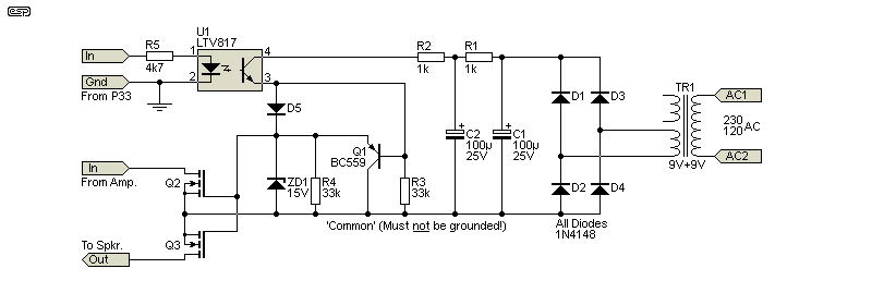
BY default (no LED current) the MOSFETs are turned off, and they are turned on after the P33 delay has expired - provided there's no DC present at the amp's output. MOSFET selection is important, as this determines the dissipation with an audio signal. If a MOSFET has a RDS-on of 44mΩ (IRF540N) and the amplifier has a supply voltage of ±50V, the worst-case peak dissipation is 550mW, with the average being much lower (generally less than 100mW). Note that the MOSFET's voltage rating must be equal to or greater than the supply voltage. In theory, that means the IRF540N can be used with supplies up to ±100V (I suggest no more than ±60V), but a lower RDS-on would be wise. See below for more details on suitable MOSFETs.
Q1 (shown as a BC559) is not critical, and you can use any small-signal PNP transistor that you have available. The transistor (along with D5 and R3) create a fast turn-off circuit, ensuring that as soon as the optocoupler output falls to zero, the MOSFET gates are discharged. It's possible to simplify the circuit by replacing D5 with a link, and omitting Q1 and R3. MOSFET turn-off time is increase by about 0.5ms - not much, but it reduces the instantaneous dissipation in the MOSFETs if there's a DC fault. All resistors are ¼W and can be metal film or carbon. The transformer (and the MOSFETs) are the only parts that need to be as specified - the transformer to ensure proper isolation between channels, and the MOSFETs to ensure minimum signal loss and a safe operating area that will handle turn-off under fault conditions.
You can (if desired) use a small-signal P-Channel MOSFET such as a BS250P in place of the BC559, but there's no advantage and it's far more likely that you'll have a PNP transistor than a p-Channel MOSFET in your parts drawers. The MOSFET is also (slightly) more expensive, but we're only looking at a few cents. Of course, the MOSFET requires more careful handling to prevent gate damage from ESD (electrostatic discharge), and the same applies to the main switching MOSFETs.
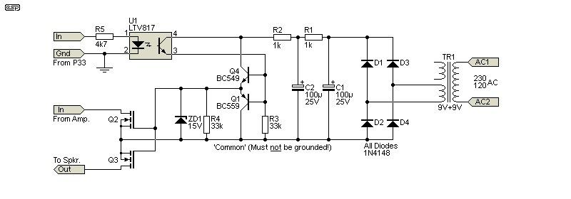
If you think you'd prefer a 'totem-pole' gate drive circuit, it's shown above. The diode is exchanged for an NPN transistor, but the number of parts is the same. The turn-on time is lower, but that's not a particular advantage for this application. The totem-pole gate driver is a well-established technique that's been used for many years. The Fig. 2 version works much the same way as the other, except that the opto only supplies base current to Q1, and doesn't have to supply the full gate current.
The only real advantage to the Fig. 2 circuit is that the optocoupler output current is much lower, as it only supplies the bases of the transistors (along with R3). This means that you may get away with an optocoupler with a relatively low CTR and/ or use a lower LED drive current. 5mA is still the recommended current, so I leave the decision to the constructor. If (and that's a big 'if') a PCB is ever developed, I'd probably use the Fig. 2 version, but the difference in real terms is minimal. I know that the Fig. 1 version works perfectly, because I built and tested it. It does have a greater turn-on time, but that is of no consequence in use.
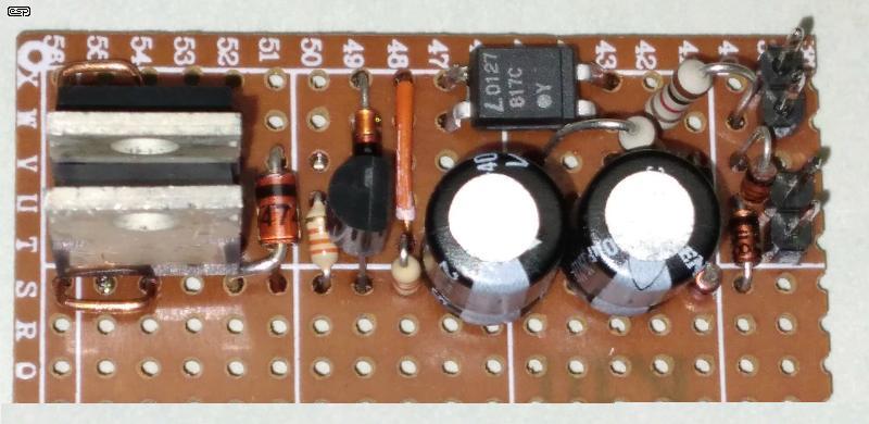
A photo of a single channel is shown above. It's roughly 5 times the size of the actual circuit. The piece of Veroboard is 48mm long by 20mm wide, and it should be possible to build two on a 35mm wide board. I've only shown the populated area, but the piece of Veroboard I used is 35mm wide and it's easy to see that two will fit. The wire loops on the right connect to the MOSFET drains. On the right side, there's the connection for the optocoupler at the top, with the 9V connections directly below (separated by one empty hole). The board would need to be a little longer bigger if you use TO-247 MOSFETs. With a wire jumper between the input pins so that only one pair of 'trigger' wires is needed. I included a 1k resistor in the opto's LED input, because I used a 5V trigger for my tests, and some degree of current limiting is needed to prevent accidents.
Needless to say it has been extensively tested, and performs exactly as described. I used IRF540N MOSFETs in the test circuit, which means they have a total 'on' resistance of less than 0.1Ω (theoretically 88mΩ if the datasheet specification is accurate - it's usually a 'typical' figure. My low-resistance meter says 68mΩ which is slightly better than expected.
Of course there's also the transformer, and the one I used measures 30 x 25 x 22mm (excluding pins). Because it's a PCB-mount transformer it needs a piece of blank fibreglass or similar for mounting. Do not use Veroboard, as it's too hard to ensure proper isolation of the mains. with all the narrow-spaced tracks.
The power supply relies on the very poor regulation of small transformers. The 9V winding of a 1.5VA transformer will provide a no-load voltage of about 13-14V, and the one I used provides an unregulated voltage of about 19V DC, rectified by D1-D4 and smoothed by C1. R1 reduces ripple via C2 (creating a simple π filter). The ripple at the the positive end of C2 is less than 2mV when the optocoupler is turned 'on'. R2 isolates the supply from the zener diode (ZD1) and the zener reduces ripple to almost nothing. There will be some zener noise, but it's doubtful that you'll ever hear it. The zener diode is essential to protect the MOSFET gates from damage, as it limits the peak voltage.
With U1 turned off (no input current), the base of Q1 is pulled to common via R3, and the MOSFET gates are pulled low by the emitter of Q1 and R4 (the latter is not strictly necessary, but it would be a mistake to leave it out). When the optocoupler is turned 'on', voltage is applied to the MOSFET gates via D5. The circuit 'trickery' is when the opto is turned off due to a fault, but this only applies to the Fig 1 version.
The MOSFET gate capacitance will discharge via R4, but mostly due to Q1. The base is pulled to common almost instantly (less than 50μs), which causes the emitter voltage to fall. It's the emitter of Q1 that discharges the MOSFET gate capacitance. I tested it with 120nF (far greater than any MOSFET), and the discharge time was consistently below 100μs. Without Q1, the discharge time can be much greater than we'd like, and this is the 'trick' circuit. It's unconventional, but it works as intended and is a cheap alternative to a dedicated gate driver circuit (whether discrete or integrated).
Note that the Fig. 1 gate drive circuit is unconventional. Voltage is applied by the optocoupler and D5, and when it's removed, Q1 speeds up the discharge of the gate capacitance. When the opto turns off, Q1's base is pulled to ground (actually 'common' it must NOT be grounded). Q1 then turns on to discharge the gate capacitance. This reduces turn-off time dramatically. A more 'traditional' totem-pole (2 x BJTs, one NPN and one PNP. Fig. 2) will drop slightly more gate voltage than the Fig. 1 shown, and offers no real advantages or disadvantages. Use whichever version you like.
In both circuits, the MOSFETs are turned off with a PNP transistor and a resistor. The turn-off time can be less than 10μs. Ultimately, the 'off' time is dictated by the optoisolator, not the drive circuit. The turn-off time is tiny compared to the detection time of a DC fault by P33 (or any other fault detector) and will never be a problem.
Note: When a speaker is suddenly disconnected due to DC, any inductance will create a back-EMF, proportional to the inductance and current. This can (in theory) reach a very high voltage that may cause avalanche breakdown in one of the MOSFETs (polarity dependent). The MOSFETs used should provide a guaranteed avalanche rating of not less than 200mJ (millijoules). To give you an idea, if the MOSFET is subjected to an avalanche of 100mJ for 100μs, that's the equivalent of 1kW across a 100μs period. See Loudspeaker Back-EMF (below) for more details.
One thing that's critically important is to get the LED current right for the optocoupler you use. The CTR (current transfer ratio) will be far lower than expected if the current is too high or too low. High current should be avoided because the life of the LED is reduced as you approach the maximum allowable current.
The LTV817 or 4N25 has a maximum CTR of unity (10mA LED current gives 10mA transistor collector current), but that's not going to happen in reality. Mostly, expect a maximum of between 2-5mA through the transistor for 10mA LED current. Note that some optocouplers have a much better CTR, others worse. For example, the CTR of the LTV817 will be between 50 and 600% with 5mA LED current. All my bench tests used a 5mA LED current. Many optocouplers are 'ranked' for CTR, but mostly you'll just get whatever is readily available. The LTV817C (which I have) has a CTR between 200 and 400%.
There are many other optocouplers you can use, and I used the LTV817C, a 4-pin device designed for high density layouts. This is unimportant in the greater scheme of things, as we only need one for each relay, but I have them in stock. They have a minimum CTR of 200%, so 10mA of LED current will provide up to 20mA peak gate current. Most will be much better than this, but 5mA is quite sufficient. Turn-on is not likely to be an issue, regardless of the optocoupler.
The power supply circuit is conventional, but it does rely on the poor regulation of the small (1.5VA) transformer. Those I suggest have an output of almost ±20V (14V RMS) with no load (for a nominal 9V transformer), and this is more than enough to turn on the MOSFETs. Perhaps surprisingly, the ripple voltage on the gate supply is important. If there is significant ripple, this will cause channel modulation, adding a 100Hz tone to the audio. With the arrangement shown, the ripple voltage is very low (well under 1mV), so modulation is negligible.
If you use a larger transformer than the one I used, you will need to select a higher voltage for the secondary. Anything from 12 to 15V is alright, but C1 and C2 need to be a higher voltage rating. With a 'stiffer' power supply, increasing the values of R1 and R2 is recommended to limit the optocoupler current. Determining appropriate values is probably best left to experimentation, as there are too many possibilities. Be aware that the isolation voltage between the secondaries must be specified in the datasheet, because that insulation barrier separates the two power amplifiers from each other - assuming that you use a common transformer for both MOSFET relays.
Feel free to use a 12V transformer, as that will provide a higher no-load voltage. While this makes filtering a little easier (because there's more voltage to 'play with', it also means that the caps need a higher voltage rating. 25V caps are ideal for the version using a 9V transformer, but they'll need to upgraded to 35V with 12V windings.
Overall, the turn-off time (and dissipated energy) is short enough to ensure the MOSFETs will survive. Ultimately, you always need to run tests with anything like this, because a MOSFET failure could still cause speaker damage - the very thing you're trying to prevent. Like most semiconductors, MOSFETs fail short-circuit. As with the previous MOSFET relays I've published, proper selection of MOSFETs will provide excellent protection for almost any speaker combination you're likely to come across.
The MOSFET depends on the amp power, but a device with low RDS-on will always give the best results. One that I can recommend is the FDP083N15A, rated for 150V, 117A, 294W (at 25°C), 8.3mΩ, in a TO-220 package. These aren't especially cheap, but they are far cheaper than a loudspeaker. The high power rating is of little consequence, but the RDS-on of 8.3mΩ means that very little power will be 'lost' across the MOSFETs. These also have a very healthy 542mJ single-pulse avalanche rating!
Another good candidate is the IRF150P220, but it's fairly expensive. Rated at 150V, over 200A and with an RDS-on of only 2.7mΩ (maximum), it should withstand anything you can throw at it. The single-pulse avalanche rating is 835mJ, way beyond anything a speaker can produce.
Beware of inductive loads! Most speakers have some inductance, but it's usually fairly lossy and is often more accurately described as a semi-inductance. The peak power in the MOSFETs can reach over 2kW with a 60V supply and a 'pure' inductance of 1mH, but with a more realistic circuit (inductance in series and parallel with resistance) this should be below 400W for less than 10μs. Simulated with a 'typical' speaker/ crossover combination the dissipated energy is quite low - this has been confirmed with bench testing.
It's worthwhile to look at the back-EMF from a 'typical' loudspeaker. I ran bench tests and simulations, and with conventional speakers, the back-EMF is not as high as you might imagine. When an inductive load is disconnected from a DC supply (your amplifier if it develops a serious fault), there is an inductive 'kick' - this is back-EMF. However, most speaker systems are fairly low Q (quality factor - as applied to inductance, not sound quality), and the inductive back-EMF is fairly low. There is also an expectation that the MOSFET turn-off time will be at least a few 10s of microseconds. A measurement of the circuit shown indicates a gate voltage turn-off time of a little over 250μs, but the MOSFETs are faster; I measured 6μs for the MOSFETs to turn off in the prototype. They turn on in just 3μs.
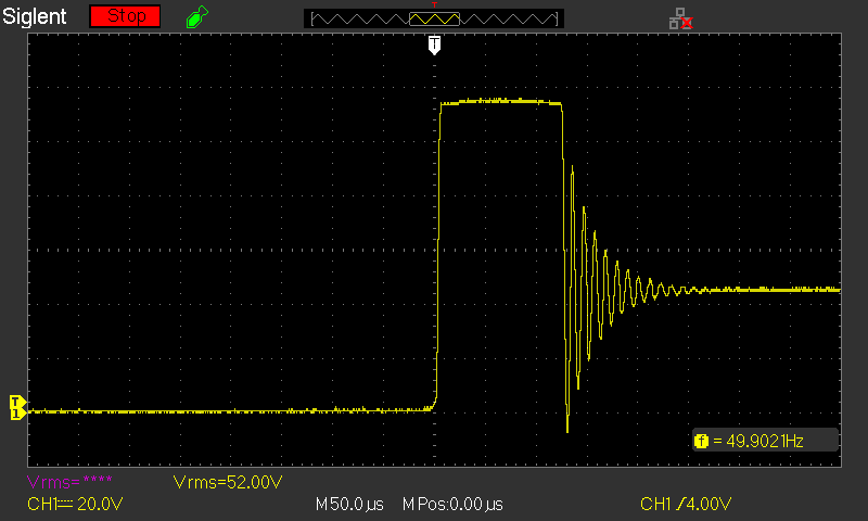
The worst case back-EMF I measured was from instantaneous disconnection of a speaker subjected to a +10V DC 'fault' for about 30ms. The reverse voltage (due to inductance) was only -55V, with most of the tests showing no more than -10V. When the DC is disconnected more slowly (around 100μs or so), the back-EMF shouldn't be greater than the supply voltage. A scope capture of the waveform (instantaneous disconnection) is shown below. I used 10V because I didn't want to risk my test speaker (one of several I use in my workshop), but the voltages scale in direct proportion. With +60V instead of +10V, the back-EMF will reach around -80V. 'Worst-case' could be up to -330V with a +60V assumed fault voltage, and this is where the avalanche rating for the MOSFETs comes into play, as the voltage will be clamped to the MOSFET's breakdown voltage. The energy stored in the inductance is dissipated in the breakdown (avalanche) region of the MOSFETs - assuming that it's great enough.
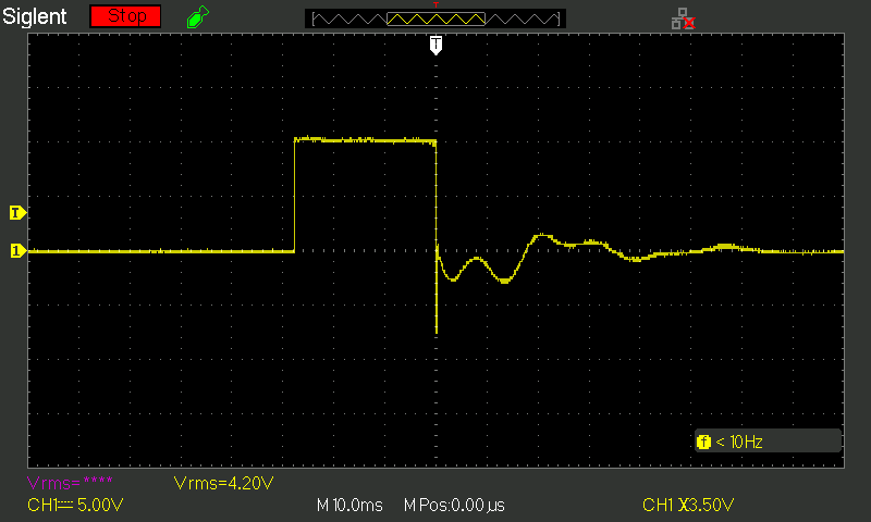
That's all well and good, but other speakers will be different, and it's obviously not possible to test them all. However, we can be fairly confident that none will behave as a 'pure' inductance, as such a speaker would give any amplifier ever made severe 'heartburn'. The width of the negative-going 'spike' is roughly 50μs. For what it's worth, the energy stored by an inductor is equal to ...
Energy (Joules) = ½ L I ² So, for a 20A fault current and a 1mH inductor ...
E = 0.5 × 1m × 20 ² = 200mJ
The above will always be reduced due to the effects of parallel resistance and/ or capacitance. Without knowing the exact details of a loudspeaker you can't estimate it, but it will be reduced to a more manageable value with the vast majority (if not all) loudspeaker systems. So, at least in theory, a high avalanche rating isn't essential, but under-specifying the MOSFETs is not advisable. The FDP083N15A I suggest is fine for amplifiers having a supply voltage of up to ±100V (over 600W into 8Ω). They have an avalanche rating of 75A for 45μs at 25°C - a figure that will be very hard (if not impossible) for any speaker system to create.
You can get a (very) rough idea of the inductance by looking at the impedance. When it's rising with increasing frequency, that's inductive reactance. Much of the inductance is due to the bass driver's resonance peak, and although it has a fairly low Q there's a moving mass that generates voltage. You can't get a realistic idea of the potential back-EMF by tapping on the cone, as it's not possible to get high enough acceleration. You might be able to measure the (semi) inductance with an LCR meter, but most probably won't give a very accurate reading.
Given the potential severity of back-EMF, I decided to run some serious bench tests, much worse than you'll get from any speaker. It was hoped that I could destroy a MOSFET by pushing the limits, but to no avail; MOSFETs are tough! I used a 2mH air-cored inductor, operated at a current of 5A with a voltage of around 45V DC. I tested with a parallel resistor (1k) and no resistor at all. The theoretical energy stored is 25mJ, which is far greater than I'd expect any loudspeaker to reach. The MOSFET avalanche region was easy to see - the waveform flat-topped at the breakdown voltage (just under 120V for 100V MOSFETs).
The avalanche period is 120μs, with the current limited by the 8Ω load resistance. The instantaneous power of the identical circuit was simulated to be 550W. Unlike a normal speaker protection circuit, this test was performed multiple times, often with only a few seconds between tests. I 'finger-tested' the MOSFETs, but the one in avalanche only got slightly warm, even after repeated tests. Considering that I used a pair of IRF540N MOSFETs (for a 'worst-case' test, with only 13mJ avalanche rating), it's safe to say that the ones I recommended above will be more than acceptable.
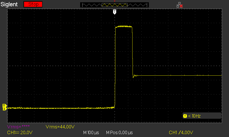
When a 1k resistor is added across the inductor, the ringing seen above vanishes, but the instantaneous power was the same. The simulator again gave an almost identical result. It's understood that a 'real' speaker system will almost always have a lower impedance than the 8Ω I used, but from the tests I performed a speaker is also a much less savage load than an air-cored inductor with minimal damping. When I used a 10Ω resistor in parallel with the inductor, there was almost no back-EMF to be seen.
Note that the time scale for Fig. 6 is 100μs/ division, but is 50μs/ division for Fig. 5. The total load resistance was also a little over 8Ω because of the resistance in the inductor and my test leads. This changes very little in terms of the results obtained. This information was not provided for the other two projects, but they have been updated with a link to this section.
This circuit is provided as an alternative to the other two I've already published. It will occupy more space because of the transformer, but overall the total cost will be roughly equal to the other two. The biggest difference is that there is no PCB available - subject to change if there's enough interest. There are no SMD parts, and if necessary you'll be able to repair it in 10 year's time because it uses no parts that will become obsolete and irreplaceable. The MOSFETs you use may disappear at some point, but there will be replacements that may even be better than the ones you use.
The transformer is a nuisance, but any MOSFET relay requires a power source to power the gates, and a small, low-cost mains transformer is the most basic (but easiest to understand). It uses more parts than the other two published circuits, but they are all common and cheap. The electrolytic caps may fail eventually, but given the tiny ripple current they will probably outlast you - provided they are not near a heat source.
The circuit might look complex, but it's easily built on Veroboard, and is simpler than it appears. You need two for a stereo circuit, with the second channel powered from the second transformer winding. It uses low-cost parts throughout, and it requires no parts that will ever become obsolete. This may never be an issue with the previously published circuits of course, but there's always some comfort to be had when you know that the parts are not just readily available, but might already be in your parts drawers.
There is an optocoupler that's pretty much perfect for this project, the VOFD343A. It uses an advanced gate drive circuit and includes proper gate protection, and is very fast-acting. The latter is actually more of a curse than a blessing - it minimises switching time, but that means the inductive spike will have more energy. With suitable MOSFETs this is unlikely to cause any issues of course, but it's something that has to be considered. So, why didn't I specify this part? Two reasons, with the first being that it's SMD only, and the second being that it may not be available in 20 years time. One of the primary reasons for this design is that it uses 'legacy' parts that are unlikely to become unavailable in your lifetime.
While the primary reason for this (and the other) MOSFET relays is for speaker protection, they can also be used for 'general purpose' speaker switching. This would normally be done using traditional electromechanical relays, and these are a more sensible option if one never needs to interrupt DC at more than ±30V. With appropriate MOSFETs, you can switch any AC or DC load with a fully isolated switching system such as that described here or in the other two MOSFET relay projects. Like the Project 245 circuit, this version can also be used for 230/ 120V AC switching (with high-voltage MOSFETs), but the switching is not quite fast enough for use as a leading or trailing-edge dimmer.
Isolation is the responsibility of both the mains transformer and the optocoupler. This is usually not a limitation unless you want to do something unusual. If this is the case, it's your responsibility to ensure that all wiring and insulation is up to the task. While this is a low-cost circuit, it will still cost more than an electromechanical relay (EMR), and it will probably only be used where a DC circuit must be broken, something that EMRs are no good at if the voltage exceeds 30V.
There are no references, other than Project 198 and Project 245. Everything involved uses basic principles, although the gate-drive circuit may be unique, as I've never seen this arrangement used elsewhere.
 Main Index
Projects Index Main Index
Projects Index
|