
|
| Elliott Sound Products | Lock-In Amplifiers |
 Main Index Articles Index Main Index Articles Index |
I suspect the first question will be "WTF is a lock-in amplifier?". Fair question, and it's certainly not something that everyone needs. Indeed, most people will never have heard the term, so it's something that needs a good explanation. A lock-in amplifier (LIA) is designed to extract a usable signal from one that's otherwise almost all noise. Traditional lock-in amps have a DC output that's proportional to the 'buried' signal's amplitude. This may not be considered 'acceptable', but when you read an AC voltage on a meter, that's been converted to DC first anyway. We accept that (almost) without question, so there's no real reason to be suspicious of an instrument that simply produces a proportional DC signal.
Lock-in amps are a stock item in many laboratories, where there is often a requirement to measure signal levels that are so low that noise becomes the predominant factor. With a digital oscilloscope, it's sometimes possible to use the averaging function to see the waveform, but you need the scope to be triggered from the original (noise-free) input signal. Without that, the averaging process will fail because there's no fixed reference. This is demonstrated further below.
The LIA also uses averaging to obtain a DC voltage that represents the amplitude of the output, but without the noise. It's not just broadband (thermal) noise that will be removed - 50/60Hz hum and other unwanted frequencies will also be eliminated. It's common for lock-in amps to include notch filters to reject mains hum, but they (like all filters) introduce phase shift that can make the output voltage unpredictable. Actually, it is predictable, but only if you know just how much phase shift has been introduced so it can be compensated.
Early lock-in amplifiers were (predictably) all analogue, with the earliest versions using valves (vacuum tubes). The design is credited to Robert Henry Dicke (1916-1997), although this may be disputed. The first commercial LIA was developed by Princeton University and the Plasma Physics Laboratory in 1962. This was the model HR-8. One of the major suppliers today is Stanford Research Systems, but there are plenty of others.
You can buy a lock-in amplifier from eBay for around AU$100 AU$200 (the price mysteriously doubled as this article was being written), and it's just a PCB with an AD630 (Balanced Modulator/Demodulator) from Analog Devices, plus a couple of opamps. The AD630 datasheet even includes the circuit for an LIA, and I suspect that the eBay version follows the circuit shown reasonably closely. The price seems high, but if you buy an AD630 from a distributor, that IC alone will cost roughly half the cost of the complete PCB. Is it any good? Quite frankly I was astonished! It's very good indeed!. Similar (and identical) units are available from several other on-line outlets, invariably in China at various prices.
. It uses an AD630, with an OPA627 opamp with a gain of 10. It can be re-configured as a balanced modulator by changing the positions of a couple of 0Ω resistors. In3 is not used.")
I ran a test with a voltage divider that gave me 10μV (RMS) with a 2V input signal (a similar but slightly different attenuator was used for the scope capture), and I tested the module (after a calibration pot) at a number of frequencies, and down to 1μV input. The output is calibrated to provide 100mV DC for a 10mV RMS signal, and I used my low-noise test preamp with a gain of 60dB (×1,000) in front of the module - a total gain of 10,000 (80dB). With 10μV in, the signal after the preamp was full of 50Hz hum and broadband noise (see scope capture further below), and the output from the LIA was rock-steady at 98.7mV - that's 1.3% accuracy, measuring a 10μV signal. There's a zero-signal DC offset of about -100μV from the LIA, so your input signal must be high enough to make that irrelevant (I suggest ≥100mV of signal if possible).
If this happens to be something you desperately need (or just want), the module shown will take some beating. Obviously, I cannot vouch for specific eBay sellers nor make recommendations because things can be unpredictable, but if you get one that works properly you won't be disappointed. You will need a low-noise, high-gain preamp, and you need at least 60dB gain (switchable) for it to be useful. If there is sufficient interest I'll put together a project version of the complete system. The module I bought will be assembled into a case to become a complete (albeit basic) lock-in amp that I can use when I have very low voltages to measure. It won't be used very often, but it most certainly will be used!
The circuits shown below have been simulated, and they don't show everything in detail. The multiplier version is pretty easy, because it's only an 8-pin device and it's not ambiguous. The synchronous rectifier is trickier, because it's shown 'in principle' rather than a complete design. However, there is a version of the AD630 modulator/ synchronous rectifier shown as a complete circuit. That was adapted from an application note, and should work as shown. For anything else, you need to add amplifiers, DC offset correction, filters and phase correction to suit your specific application.
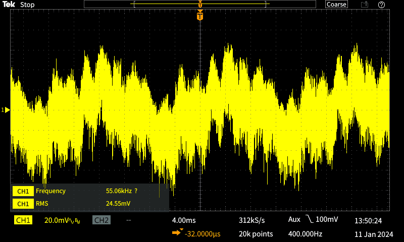
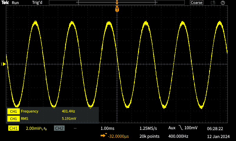
Mostly, if we need to measure a noisy signal we'd use a scope with averaging. My test setup used a 1V, 400Hz signal, with a direct feed to the scope's external trigger input. Triggering was set to use the external input, and I was very careful to ensure that triggering was 100% reliable. The signal was attenuated by a factor of 185k, using a 500k resistor feeding 2.7Ω The voltage across the 2.7Ω resistor should be 5.4μV. The left-hand capture was done with a 4ms/ division timebase, the right at 1ms/ division. 50Hz (20ms period) is quite visible on the left capture. Note that averaging with a scope depends on the scope itself. Some do a poor job, even if set up properly.
The 5.4μV signal was passed through my low-noise test preamp (see Project 158), with the gain set to 1,000 (60dB). Predictably, the output from the preamp should contain 5.4mV of the wanted signal, plus vast amounts of 'stuff' we don't want. There's thermal noise aplenty, along with 50Hz hum. I quite deliberately didn't shield any of the outboard circuitry (two resistors plus scope probes and clip leads) because I wanted to see how much hum was picked up, even at such a low impedance. The non-averaged trace shows 25mV of noise, with 5.4mV at 400Hz hiding within after amplification. The 400Hz signal is (more-or-less) visible, but it's overwhelmed by broadband noise and 50Hz hum. Reading the voltage is not possible with all that noise.
The 5.4μV output is amplified by 1,000, but that leaves the signal obscured by noise and hum. Averaging makes the signal and its waveform visible, but if there are cycle-by-cycle waveform variations, they too are averaged, so what you see is not necessarily the signal as it really is. It might be, but you can never know for sure. This is similar to reading the voltage with a meter - you see only the amplitude, and have to guess at the waveform. This is why we use scopes, but they can't measure such tiny voltages without external circuitry and averaging.
 |  |
Note: Hover over the image to see the full sized version
The recovered waveform using averaging is more-or-less what one would expect, but the amplitude is a little low. I don't know if this is an artifact of the scope's averaging process, but I know that the reading should have been 5.4mV. The scope shows 5.2mV with 64 averages (which seemed to be the 'happy place' for this measurement). I think this is just acceptable, particularly when you look at what was retrieved after the ×1,000 preamplifier. It shows that the signal is present and at least close to the expected value, with most of the noise eliminated. This can't be considered a bad result when you look at what I started with. 5.4μV - that's not much! While averaging certainly works (provided it's available on your scope), there's a fair bit of messing around to get the triggering to be perfect, and you need to wait for the average to settle. Any disturbance during the averaging period causes it to mess up and start over, which can become tedious.
Measurements of such small voltages that are buried in noise will always be a problem, and the LIA is the most effective solution to date. Scope averaging works quite well with less noise, but the limitations are obvious. I set up a crude multiplier circuit to measure the voltage using the technique described below, and that gave a result of 5.46mV. I suspect that most of the error was due to DC offset - I included an offset adjustment pot, but setting it accurately is a chore (due to the integrator).
If you use a lock-in amplifier you have to be 100% confident that it has no DC offset, and that the displayed voltage is within expectations. A multiplier wired up on a bit of Veroboard with wires everywhere doesn't quite qualify (the multiplier board is for another project), but with a system that's set up properly you have the ability to measure voltages that would otherwise be quite impossible. My experiment wasn't quite an unqualified success, but it does show that the process works, even as a lash-up.
Using the Fig 0.1 module was significantly more successful than my test multiplier, even though there were still cables all over the place. On this basis, I'd have to recommend synchronous rectification over the multiplier approach, although there's no reason that a fully developed multiplier-based LIA can't be just as good. The two techniques are explained below.
The nice thing about AC is that it is AC, so at normal signal levels (and impedances) the results are generally unambiguous. If there is a DC offset it can be removed by using AC coupling on a scope or by adding a capacitor to the output of the circuit under test. When your signal is DC, there's no problem with normal supply voltages and small inaccuracies rarely matter much. When a measurement system provides a DC output to represent AC, DC offset becomes a real problem, especially at low levels. When your signal is only 5mV DC or so, otherwise inconsequential DC offsets can cause a very large error. An offset of only ±50μV with a 5mV signal is 1%, which may be your entire error budget!
Note: When taking a measurement with a scope or an LIA, the waveform from the preamp (including noise) must remain within the dynamic range of the scope's input preamp or the multiplier. If noise peaks exceed the allowable dynamic range (i.e. there's [internal] clipping), the reading will vary between wrong and terribly wrong!. The scope is especially vulnerable, because when averaging is selected, you see the average, and the peaks are 'invisible'. You will probably be tempted to increase the gain to get a better waveform, and while you will see a higher level, it will be wrong. How do I know this? Predictably, my first scope tests gave me answers that were clearly incorrect, and the reason was realised fairly quickly. I tell you this so you don't make the same mistake.
While I have only covered low frequency operation, lock-in amps are available with frequencies up to 200MHz, although most are limited to 250-300kHz. The principles don't change, but phase alignment becomes critical. Many are also fitted with VCOs (voltage controlled oscillators) using phase locked loop techniques, and this allows for the measurement of harmonics. Many commercial instruments also include a quadrature detector, allowing phase to be measured. These are not covered here, so if you're interested you have lots of external reading to do.
Not all wanted signals are very low level, but that doesn't always mean that they're not noisy. The general principles work just as well with 1V as with 1μV (mostly better), but the most common use for lock-in amps is to extract a low-level signal from a comparatively large amount of noise. The 'noise' may not even be standard random ('white') noise, it can just as easily be a strong interfering signal or series of signals that are too difficult to filter out. In electronics (and to our ears) anything that we don't want to see or hear can be considered noise.
Noise is the enemy of all low-level measurements. It's a problem with both AC and DC, but AC is worse because the wanted signal is in amongst broadband noise, which spans a frequency range dependent on the measurement bandwidth. You can filter out the noise, but this can be difficult because narrow-band filters require a high Q (quality factor), and they have an extended settling time. Ensuring that the gain remains constant as the frequency is varied can also be a major challenge. The waveform is also changed, so what started as a squarewave will look like a sinewave if the filter is sharp enough. This isn't always a problem of course. DC is a little easier because an 'extreme' low-pass filter will remove most noise but allow the DC to get through. However, with DC you have other problems, notably opamp drift and other physical effects that create offset voltages that are often temperature dependent. Amplifying DC is covered in more detail in Section 5. Unfortunately, even comparatively small amounts of noise can make AC measurements difficult to interpret with accuracy.
Believe it or not, the next graph shows 70mV of 400Hz signal, 700mV of 50Hz hum and 1V of random noise (all values are RMS). The 50Hz component is quite obvious, as is the broadband noise. An LIA will have no difficulty extracting the signal (as a DC voltage) and almost complete rejection of everything else. This is almost impossible with any other method. Not being able to examine the wanted signal's waveform is a limitation, but it's not a game-changer. Having confidence that the DC output accurately represents the signal voltage is far more important for many measurements that are undertaken under extreme conditions. This is the signal I used for some of the simulations. The total voltage is 1.4V RMS.

In almost all cases, the reference and the wanted part of the 'dirty' signal are (or are assumed to be) sinewaves. You can't use a lock-in amp to look for waveform distortion through the DUT, because it can't be done. The output is DC, and while another multiplier can reproduce a sinewave of the same (or amplified) voltage as the input, it's fake. It may look the part, but the actual waveform may be badly distorted, and you won't know. This is where using a scope with averaging can save the day - provided the distortion is consistent from cycle to cycle over the averaging period (which may be from 2 to 1024 waveform cycles).
Unlike 'normal' voltage measurements where we can see the output immediately (or close to it), any system that uses averaging will take a long time. Greater accuracy is obtained by taking more averages, so you may not get a steady signal for 5 seconds or more. These are not everyday techniques though, and if you have 1μV of signal it must be amplified first so the multiplier has enough signal to work with, and in this case you'd need at least 100dB of gain (×100k). That gives a signal level of 100mV, but expect at least 31mV of noise from the amplifier (assuming a 'perfect' amplifier with 100kHz bandwidth and an input noise of 1nV√Hz), plus noise generated by the signal source and picked up from the surroundings. The total noise could easily exceed a couple of volts. Using more amplification to get a better signal level is advised, but of course that will also increase the noise.
Consider an amplifier with an equivalent input noise (EIN) of 1nV√Hz. If the bandwidth is limited to 100kHz and the gain is 60dB (×1,000), the output noise of the amplifier alone is ...
EIN = 1nV × √100k = 316nV
Output Noise = EIN × Gain
Output Noise = 316nV × 1k = 316μV
This is only for the amplifier (and 1nV√Hz is a very good noise figure). Add to this the noise from your external circuit, noise picked up from nearby switching power supplies (including LED lighting), 50Hz magnetic fields from linear power supplies, and general noise that's inevitable unless you have a very expensive Faraday cage at your disposal. If you're trying to measure even a 10μV signal, it's quite apparent that noise will dominate (see Fig 0.2A). My test preamp has less than 1.2mV of output noise with a 50Ω input termination and 60dB gain. Its bandwidth is restricted to about 50kHz (theoretical noise is ≈224μV). All external circuitry adds noise, including resistors. For an in-depth article on the topic, see Noise In Audio Amplifiers.
Noise does not add algebraically because it is random. When there are two (or more) noise sources, we use the square root of the sum of the squares. So ...
Noise = √( N1² + N2² + Nn² ) For example ...
Noise = √( 1V² + 1V² ) = 1.414V
As already discussed, the average value is zero, but to eliminate DC errors capacitor coupling is recommended. The averaging process means that you have to expect it to take time before you get a usable result. For the graph shown at the beginning of this article, a usable output isn't reached for 5 seconds. A great deal depends on low frequency noise (aka 1/f, shot or flicker). By its very nature, this type of noise increases as the frequency is reduced. It's always a part of the noise signature of opamps, and the corner frequency (where 1/f noise transitions to broadband noise) depends on the fabrication of the device. It's typically around 50-60Hz, but it can extend to 200Hz or more with some devices.
This is a pain, because it's precisely the kind of noise we don't want when integrating to obtain a DC level. Being 1/f noise, as the frequency is halved, the amplitude doubles. If you happen to need very high gain after your sensor, you can use a 'chopper' (aka zero-drift) opamp. This will effectively eliminate 1/f noise, but only that from the opamp itself. External 1/f noise is amplified as normal.
'Atmospheric' noise is a far bigger problem now than it used to be. This is due to the multiplicity of switchmode power supplies (SMPS) that power almost everything. Equipment like oscilloscopes and the like are carefully shielded internally, but problems will always arise with probes and other wiring. In theory, all SMPS have passed the required tests for conducted and radiated emissions, but the proliferation of low-cost Asian products means that we know that at least some will never have been tested and will generate far more noise than they should. Other sources include general background noise that exists everywhere, lightning, the neighbour's lawn mower, etc., etc. In short, noise is everywhere, and techniques to eliminate (or at least minimise) its influence are very useful. Enter the Lock-in amplifier.
Depending on the lowest voltage you expect to try to measure, you may (just) get away with an external gain of 1,000 (60dB), but you're more likely to need anything from 10,000 (80dB) to 100,000 (100dB). Then there's the LIA's input gain of 10, so you could easily have a total gain of 1,000,000 (1 million, or 120dB). The input noise (EIN) of the first stage will dominate, so if you have an EIN of just 1nV√Hz, that translates to 141mV of noise with 120dB of gain (assuming just 20kHz bandwidth). That should allow you to measure a signal level of just 100nV (0.1μV). Maintaining the stability of a preamplifier with a gain of 120dB will be a challenge!
The signal - including noise - must not clip! We may tend to think that the wanted signal is simply 'hiding' inside the noise waveform, that's not the case at all. With any electrical waveform, there is one (and only one) voltage present at any given time. The wanted signal is 'riding' the noise, so if the noise is clipped, so is our wanted signal. This is easy to see with just two frequencies, but it's harder to visualise with broadband noise. So, the noise signal must not be clipped, and this will often set the limit for the lowest input voltage that can be measured. Using filters will reduce the noise, but will also add phase shift, so care is needed to ensure that any phase shift is equal but opposite. Phase shifts can then cancel, without attenuating the signal (2-octave spacing above and below the test frequency is the minimum for 2nd order filters).
The basic operation isn't too difficult to understand. There are two main approaches - a dedicated phase-sensitive detector or a multiplier. Both achieve the same result, but the multiplier is (marginally) easier to understand. Multiplier ICs such as the AD633 are cheaper (although still expensive for an IC - around AU$30 each), and the description that follows is based on this IC.
When two signals of the same frequency (and phase) are multiplied together, the output is always a positive value. Their amplitudes can be quite different, and that doesn't affect the outcome, but it does alter the relationship between the (signal) input level and the multiplier's output. If the signal to be measured is DC, it's standard practice to modulate it, because an LIA can't work effectively with DC inputs. The modulation can be generated by using the reference signal synchronised to the modulator itself. For photodiode applications, a 'chopper' wheel is often used to modulate the light source (it is what it sounds like - a wheel with cutouts to 'chop' or modulate the light beam used to illuminate the photodiode).
NOTE: This is not a project, although if constructed as described it will work. There's probably very little requirement for most hobbyists to have to extract signals buried in noise. I've had to do it on occasion, but not for any audio project. Having said that, it's still interesting, hence this article.
One important point needs to be understood. The average of any AC coupled AC waveform, no matter how simple or complex, is always zero. This is why audio equipment (for example) should always be AC coupled, using capacitors or transformers to remove the DC component. If the average value of a waveform is zero, then an extreme low-pass filter will leave only the average value - zero. This extreme low-pass filter is used at the output of lock-in amplifiers.

The above is a small sample, and it's easy to show the waveforms of any number of frequencies. Each of those shown has a long-term average of zero, having been passed through a capacitor which as we know does not pass DC. The important part is 'long-term', as several waveforms (especially if asymmetrical like the one in the centre) can have a DC component that takes time to settle.
A simulation of the basic circuit shown in Fig 1.3 was done, using an input of 100mV at 500Hz, 1V of random noise with a 100kHz bandwidth, plus 1V of 50Hz. The output is amplified by 10 to get a 500mV nominal output level. There are six samples, and each is different because the noise is random. After 5 seconds, the output is passably stable and the measurement is accurate to about 10%. A much longer averaging time will improve that, but the simulations become such that it takes too long to get a result. If the averaging time is extended by a factor of 10, you can expect the error to be reduced, but it's not a linear relationship. Waiting for 30 seconds to get a reading sounds alright, unless you need to perform perhaps hundreds of measurements!
The waveforms shown below used an EIN (equivalent input noise) of 5μV with a 1μV 400Hz signal. The signal was amplified by 120dB (1,000,000), and filtered with 2nd order filters at 10Hz and 25kHz. A usable average is reached in 800ms, and the fluctuations due to noise are less than 2% - an overall accuracy that is unthinkable using any other method. If the input voltage is reduced to 100nV, the accuracy does suffer, but you should be able to get a measurement within 5%. That can be improved by using closer filters (set for 100Hz and 1,600Hz for example) and a longer averaging period.

The noise signals (random noise plus 50Hz) aren't affected by a phase-sensitive detector (unlike the signal) because the frequencies are all different. They remain effectively random, uncorrelated and retain their zero voltage average. Noise is only amplified when the reference voltage is non-zero (any voltage multiplied by zero is zero). The noise is modulated by the reference signal, but doesn't change its average value because the two signals are unrelated. Note that expecting to retrieve a signal at 50/60Hz is unrealistic, because the signal and mains hum will correlate when they are in phase (and this will happen). This includes test frequencies that are within 10% of the mains frequency (you'll still get interference, but the average remains correct.
Note that the deviations seen in Fig 1.2 are somewhat exaggerated due to the characteristics of the simulator's noise generator. In what's laughingly known as 'real life' you will still see deviations, but hopefully they won't be as extreme. A great deal depends on the low frequency content, and at least some of it can be removed with a filter (see below for more details about the use of filters). Restricting the bandwidth (to around 20kHz for example) will also have a large impact on the noise, and will help greatly for low-level measurements.
In operation, an LIA is only usable for tests where an input signal is used to drive other circuitry, the output of which is very low amplitude. When I say low amplitude, we are referring to an output signal that may be well below 1μV, making it very hard to measure because thermal noise (as well as other man-made noise) will completely swamp the signal we wish to examine. This is something I've had to do, but it was for a project for a university. I don't have a lock-in amplifier, but the university does, and much of the original data I had to work with was measured using it.
Needless to say, this elevated my curiosity to the point where I had to know more, so that's why this article was written. I have no idea how many people will be interested, but gaining some 'new' knowledge can never be a bad thing. Apart from anything else, while you may not need to know any of this now, there may come a time in the future where you find yourself with a signal that's embedded in noise. That's exactly what an LIA is for.
As already noted, you can't use an LIA to resolve a signal that has no reference. They can only be used where your circuit/ device under test requires an input signal, and has an output that is the direct result of the input you provide. An example might be a LED driver (input) and a photo-diode (output), and indeed this is one of the areas where they are commonly used. The output from photo-diodes (and other photo-detectors) can be tiny, and noise will be a serious problem for measurements.
A lock-in amp has two inputs, one for the output of your signal source (the reference), and one for the output of the device under test. It's the reference that makes all the difference, in the same way that triggering a scope from a signal generator and using averaging for the DUT's output can remove much of the noise (this also provides a clue as to how you can often measure noisy signals with good accuracy without an LIA). The integrator shown has a -3dB frequency of about 0.6Hz.

The principle is deceptively simple. The two signals are applied to the inputs of a multiplier. One input is 'clean', direct from the signal generator and the other is 'dirty', with broadband noise, hum (50/ 60Hz) and other noises. Of the multiplicity of different frequencies at the second input of the multiplier, only one has no (or minimal) phase shift and is at the same frequency as the noisy signal. That signal is your circuit's output. The voltage can be as low as a few nanovolts, or it may be a current that's converted to a voltage with a transimpedance amplifier. The amplifier shown in Fig 1.3 could have a gain of 1,000 (60dB) or more, depending on the output signal from the circuit under test.
A system I worked with had an output current of around 120pA (yes, picoamps), and produced an output of about 150mV. Transimpedance amplifiers (V/I) are quoted as having a gain of volts per amp, and this had a gain of (and no, this isn't bullshit) 1.23GV/A. Without an ultra-quiet opamp for the current to voltage converter (transimpedance stage) and severe filtering to remove out-of-band noise, the output was pretty much unusable. The only way to get a reliable result was to use a lock-in amplifier.
At the wanted signal frequency, the multiplier has only two signals that are in-phase and at the required frequency, and these are multiplied together (effectively squared). When a signal is squared, it has one polarity - positive! All other frequencies are uncorrelated with the input signal except for instances of time when they just happen to coincide. These 'coincidences' are random, and if averaged, they will eventually cancel.
But what of the noise? It passes through the multiplier, but it's not squared, so will still have an average value of zero. All AC waveforms that are capacitively coupled have an average of zero, regardless of signal 'complexity'. 50/ 60Hz hum is also uncorrelated, and it also has an average value of zero. In short, any input that is not at the same frequency and phase as the reference is subjected to averaging, and has an average of zero volts. Only the wanted signal can pass.
For visibility, the 'noise' is a 50Hz sinewave and the signal is a 400Hz sinewave at 100mV. The reference voltage is 2V (400Hz), as this conveniently removes the 'divide by two' action of the multiplier. The 800Hz signal is a sinewave, but it's not symmetrical around 0V, it's symmetrical around the average DC - which is 100mV in this example.

If we take our wanted signal (400Hz) with the noise (50Hz) and multiply that by the 400Hz reference signal, we get several frequencies at the output. Multiplication causes sum and difference frequencies to be generated, so we see 350Hz, 450Hz, 800Hz and (most importantly) 0Hz (DC). 400Hz multiplied by itself will output the sum (800kHz) and difference (0Hz). This is shown in the next graph. The output requires scaling so that the DC voltage represents the RMS value of the input signal. With a multiplier, the output might be divided by 1.414 to display the RMS value of 100mV peak (70.7mV).
 gives a number of 'new' signals, but the only one of interest is the DC value (100mV in this example). All higher frequencies are removed with a radical low-pass filter (an integrator).")
The DC value is directly proportional to the wanted signal and the reference, so if the signal is at 100mV and the reference is 2V (both peak values), the product is 200mV and the recovered signal is at 1/2V, or 100mV. This is a DC output, because the next stage takes the average by filtering out everything that isn't DC (clearly not possible, but we can get close).
This leaves one signal out of all the noise that has a non-zero value, and that's the wanted signal. Unfortunately, the process of squaring a waveform means that the effective amplitude is halved. For example, a 1V peak signal has a peak-peak value of ±1V (2V total), but if squared, the output is only 1V p-p (you can prove that with a calculator). The output signal has double the frequency, but half the amplitude. Importantly, it is always of a single polarity - positive (-1² is +1).
If the noise (in all forms) has an average value of zero, then an ultra-low-pass filter (having a time constant of at least one second, preferably more, signal frequency dependent) will remove all the random 'stuff' leaving you with a DC offset that's determined solely by the multiplier acting upon the signal and reference frequencies. The secret is the integrator - it must be slow enough to remove random fluctuations at the lowest limit of your measurement bandwidth.
You also need to be aware of any phase shift within your test circuit. If the phase is displaced, the wanted signal is attenuated. A rough formula is as follows ...
Vout = 1/ ( 2 × sig1 × Ref × cos(Φsig - Φref ))
Make sure your calculator is set for degrees, not radians, or the formula doesn't make sense (yes, I got caught). We need the reference and the signal to be in phase, as closely as possible. A phase shift network is often used to get the best alignment (highest output level), and this will also be necessary if filters are included to minimise the noise. These may be band-pass, low-pass and high-pass, or band-reject (notch) filters, but they will all affect the phase unless widely spaced from the test frequency. This makes the use of filters less useful than they would otherwise be, unless phase compensation is included.
Small phase differences are of no great consequence. If you include a filter that causes a 5° lead or lag, you can expect an error of less than 0.5%. Should the lead or lag reach (say) 15°, the error increases to about 3.6%. Given that there will nearly always be perturbations caused by LF noise, this is likely to be fine in practice. A 45° phase shift will cause an error of 30%, which is quite unacceptable but should not be unexpected.
Consider that a multipole filter (high or low pass) and many circuits will cause a phase displacement of hundreds of degrees, but if the signal and reference are in phase (at the inputs to the multiplier), the gross phase shift is of no consequence. A 4th order filter generates a total phase shift of 360°, or 180° at the -3dB frequency.
There is a catch if you use a multiplier such as the AD633 (most others have the same 'catch'). The output is determined by the formula Out=X×Y/10, with the divide by 10 included to prevent internal overload. However, that means that if you have an input voltage of 5μV, amplified by 60dB (1,000), the multiplier's input voltage is only 5mV for the signal. With a 2V reference (all voltages are peak), the maximum output will be 5m×2/10, or 1mV. The average is only 500μV DC, so you are working at the lower limit of the multiplier's linearity. Ideally, the input gain will be at least 10,000 (80dB) and the gain stage will have a noise output of at least 2.5mV. So, while a multiplier works as an LIA, it's probably not the best solution. The tests I performed all worked, but DC offset proved to be a serious problem, even at moderate levels.
Using a multiplier is simple, but many lock-in amps use a different technique that is (at least in theory) better from a DC offset perspective. The result is much the same, but it's achieved differently. The module shown at the beginning uses an AD630 balanced modulator/ demodulator, and this uses a squarewave to alternately reverse the polarity of the wanted signal. When the input is positive (referred to the reference voltage) it's switched straight through, and when negative, it's inverted before being switched. The result is basically a synchronous full-wave rectifier (aka a synchronous demodulator), and the output is very similar to (but slightly different from) the output of a multiplier.
There is a significant difference between a multiplying lock-in and a synchronous rectifier lock-in amp. With a multiplier, you can change the gain of the lock-in amp itself by varying the reference voltage. You must ensure that there's no internal distortion or the result will be wrong. This has no effect with the switching/ synchronous rectifier version, because the reference is only used for switching and the amplitude doesn't change the output level. It must be high enough to get reliable switching, but it cannot affect the rectified output amplitude.

I thought this would be a little harder to simulate, but as it turned out the simulation was much easier than I expected. It gave results exactly according to the theory, which is always a bonus. Because of the synchronous rectification, only an input with the same frequency and phase as the reference signal is rectified properly, and everything else remains random (at least as far as synchronous rectification process is concerned).

The red trace shows the result when the signal and reference are in phase, and the average is 0.641 'unit'. With a 90° phase shift between the signal and reference, you get the green trace, and its value is 0.447 unit. The red trace is correct, and the green trace shows a serious error. The importance of this will become clear when you read through Section 5.
As with the multiplier, the wanted level is expressed as a DC voltage, but there's one small difference. The average value of a full-wave rectified sinewave is 63.7% of the peak, not 50% as we obtained with the multiplier. There are still sum and difference frequencies (0Hz, 350Hz 450Hz) as well as the 800Hz ripple we expect with a full-wave rectified 400Hz sinewave. However, the signal is switched, so we get a whole slew of additional frequencies, extending to several hundred kHz. These are of no consequence because they are all removed by the integrator.
All other factors are the same as with a multiplier configuration. The AD630 is an expensive device (local suppliers want over AU$90 for the DIP version), but the same results can be obtained with lower cost circuitry - at least in theory. CMOS analogue switches are perfectly capable of synchronous rectification, but of course there are more ICs involved, and DC offset may be a problem. This can be balanced out with the AD630, but it's likely to be harder with a semi-discrete circuit.
The primary difference is the reference voltage. With a multiplier, it's typically a sinewave, but the synchronous rectifier requires a squarewave, with the waveform changing polarity at the exact zero-crossing point of the reference sinewave. This is easy to achieve, and it's performed within the AD630 IC.

The above circuit is adapted from an application note (AN683 - Strain Gauge Measurement Using AC Excitation), with a number of simplifications so the intent is clear. The way it works is identical to the arrangement shown in Fig 2.1, with the only difference being that the signal inversion, switching and squarewave generation are all inside the AD630. This simplifies the circuit, but as noted above, at considerable cost. However, compared to a commercial LIA it's still a bargain (although you can't expect equivalent performance).
The strain gauge is driven with a 400Hz signal which is also used to synchronise the AD630. A differential amplifier provides a gain of 1,000 (60dB), the output of which goes to the AD630. The 3-stage averaging circuit removes (most) noise, leaving a DC signal that represents the unbalance of the strain gauge. A strain gauge can output positive (strain) or negative (compression), and either can be detected easily. Note that supply connections and decoupling caps are not shown, but are obviously necessary.
The final integrator is most often a series string of three to five R/C networks, and it's important to use film capacitors. You could (maybe) get away with low-leakage electrolytic caps, but film caps are a better choice overall. There are conflicting requirements, in that you need good averaging, the impedance should be low and the cap value(s) need to be 'sensible'. High-value film caps are large and expensive, so you don't want to have to use more of them than you must.
A multi-stage passive integrator is more effective than a single stage (with higher ultimate HF rolloff, -51dB at 100Hz), but the overall resistance is higher. The integrators I used are shown as 5.1k and 2.2μF, but there's no reason that you can't use 5.6k resistors. The -3dB frequency is 2.76Hz. If you were to use a single stage, the capacitance must be larger than expected, and HF rolloff is poor. With 5.1k and 12μF the -3dB frequency is the same as the 3-stage network, but it's only 31dB down at 100Hz.
In the circuits I've shown, a simple 3-stage integrator is included, but this is not the ideal way to remove the AC component. A (very) basic R/C integrator is worthwhile following the synchronous rectifier (or multiplying) circuit to remove high frequency components, but faster response is provided by a 'traditional' 3-pole (18dB/octave) filter. This has to have a response that is well below the lowest frequency you expect to encounter - including noise!. This usually means that the filter will be slow, generally requiring at least a couple of seconds before the reading is stable.
With the values used (10k and 2.2μF), a 3-stage filter/ integrator has a -3dB frequency of 1.5Hz, whereas a single integrator using 10k and 12μF has the same risetime, with a -3dB frequency of 1.42Hz. The big difference is at higher frequencies. At 100Hz, a single-stage filter is only 37.5dB down, vs. just over 68dB for a 3-stage filter. A 3-pole active filter using the same capacitance but 33k resistors has a -3dB frequency of 0.8Hz, and is 100dB down at 100Hz (allegedly - this assumes ideal parts). This filter will be within 1% after 1 second (close enough).

This is probably one of the few places where a simple ultra-low pass filter cannot use electrolytic capacitors. There are two problems, dielectric absorption (not normally a problem) and leakage (ditto). The filter is expected to give an accurate result, and anything that compromises that is not acceptable. The networks I showed use 10k and 2.2μF, with three in series. This will be within 1% in 535ms and has a -3dB frequency of 1.42Hz. This isn't bad, but it can be improved, especially if you need to measure low frequencies (2Hz or below).
As always in engineering, we need to compromise. If we simply use higher resistance values we will get a lower frequency, but we may also get DC offset due to opamp input current, and the circuit becomes susceptible to PCB contamination, humidity, etc. Much depends on the accuracy we're trying to achieve. If we're happy with around 2% (and that's not unreasonable) we can take a few liberties. A low-cost JFET-input opamp may have an input offset of around 3mV, but that can be removed with a simple offset adjustment. If our minimum signal level after amplification is (say) 100mV, the offset represents an error of 3%. That's easily adjusted to be below a few microvolts.

The circuit shown above is a good compromise, and will provide an output level of 1% accuracy within 900ms. The circuit uses a TL071 which includes an offset-null facility using VR1, and a gain control that can be adjusted to get exactly 1V output for a 1V input (a synchronous rectifier is assumed). The gain required is ×1.1, which demands odd-value resistors. A trimpot would generally be used, as that makes it easy to get an exact output. The final integrator isolates the opamp's output from capacitive loading and creates a 100Ω output impedance.
A precision opamp is another solution, such as an OPA627, with an input offset of around 100μV without adjustment (depending on the grade of the device). If this is arranged to have gain (as required for the detector), you can kill two birds with one stone (as it were). Adding gain will change the filter very slightly, but it doesn't affect its performance.
When the recovered signal is from a multiplier, the average DC value depends on both the signal amplitude and the reference amplitude. That means that if you arrange for the multiplier to have a gain of two, the average output amplitude is the same as the RMS value of the signal. With a synchronous rectifier, the average is 0.637 of the peak, or 0.9 of the RMS value. That means that you need a gain of 1.11 to ensure that the RMS value is represented accurately.
Figure 3.2 shows the result when the signal and reference are in phase and out of phase. To get an accurate result, the phase error between the signal and reference signals should not exceed 5°. Even then there is a small error, but it's unlikely to cause anyone to lose sleep. The question is, how does phase shift occur and what do we do about it?
Note that this discussion is based on analogue filters and phase-shift delay networks. If you use a digital sub-system, you can use FIR (finite impulse response) filters, which can be configured to have no phase shift. Alternatively, you can use an IIR (infinite impulse response) filter and correct its phase with a digital delay. A digital approach requires a DSP (digital signal processor), and if you go that way much of the circuitry described can be implemented in the digital domain. Modern commercial LIAs use digital processing. This is completely outside the scope of this article, and will not be discussed any further.
With any filter comes phase shift, so for the frequency of interest you must be able to tweak the phase so the reference and recovered signals are in phase. Depending on the filter you use, the phase will be either leading or lagging. A filter will create 45° of phase shift at the -3dB frequency for each 'order'. A first order filter (6dB/ octave) contributes 45°, second order (12dB/ octave) 90° and so on.
A high-pass filter will create a lagging phase shift and low-pass is leading. A leading phase shift simply means that the output signal comes before the input (which may seem impossible, but it's true nonetheless). This is a 'steady state' condition, meaning that it takes a number of cycles of the input before the long term output is stable. A low-pass filter is leading, so the output is moved forward in time compared to the input. The three waveforms are shown below, for simple 6dB/ octave filters at a frequency of ~400Hz (the filter frequency with 10k and 39nF). When phase-shift is used, it will generally be the reference waveform that's shifted, as this prevents any more noise from being introduced to the signal.
 filters. The low-pass filter creates a leading phase shift of 90° at the -3dB frequency, and the high-pass filter has a lagging 90° phase shift under the same conditions.")
You can see how the two conditions (leading and lagging) are set up as the signal is applied from time zero (t0). It's obvious that the high-pass filter's output peak does indeed occur before the input signal peak from the second complete cycle and thereafter. This means that if you add a filter to remove noise, it may affect the phase of the wanted signal. Any phase displacement causes an error in the output as described for the multiplying lock-in amplifier.
If you need to add a filter you also need to correct the phase, so you'll need to include a phase shift network, along with an inverter. Phase shift networks are lagging, so if you need to correct a phase lag, you're in for a world of pain. It's far easier to delay the reference than it is to attempt to advance the phase. It can be done, but it's not intuitive and there don't appear to be any formulae that can be used to calculate the required advance as a time shift. You can calculate phase and arrange for a long phase shift, but the delay is not necessarily constant. I'm not going there!
You will need an inverter so you have flexibility with external circuits that alter phase/ polarity. Any phase-shift networks you add will probably require switched capacitor values if your tests are at anything other than a single frequency. Your external circuit may also introduce a phase shift that needs to be corrected, and it may be leading or lagging. Remember that the closer the filter frequency is to the test frequency, the harder it becomes to make the necessary phase corrections.
If you are measuring the output from a strain gauge or other simple circuit (and this is a good use for a basic LIA), keep the modulation frequency low (around 400Hz is ideal) as that minimises phase shifts through opamps and other circuitry. 400Hz is also high enough that if you do need to add a high-pass filter you can do so with little phase disturbance provided it's tuned to no higher than 20Hz (12dB/ octave Butterworth filter). This will cause a ~5.7° phase shift at 400Hz, resulting in less than a 1% error.
 allows the phase shift to be changed by 180° if required.")
Trying to find a formula that works for determining phase shift in a network as shown is not easy. There are several candidates, but none gives the same phase shift/ delay as the simulator shows, and I know that the simulator is very accurate with such circuits. Note that the phase-shift network is lagging (so the output appears after the input). An inverter lets you switch the phase by 180° as needed. Importantly, the phase shift (in degrees) changes depending on the frequency, but the time delay does not. If you need a 50μs delay, it remains constant with frequency. The network shown has a delay from 24μs (minimum) to about 264μs (maximum). Different ranges are provided by using switched capacitors.
The frequency where a phase shift network provides a 45° shift is calculated using the standard formula ...
f45 = 1 / ( 2π × R × C )
f45 = 1 / ( 2π × 11k × 12n ) = 1.2kHz and
f45 = 1 / ( 2π × 1k × 12n ) = 13kHz (close enough)
The delay introduced at the frequency determined by Rp and Cp (400Hz signal frequency) is determined by ...
ω = 2πf
φ = arctan( 1 / ( ω × Rp × Cp )) or if you prefer ...
φ = tan-1( 1 / ( ω × Rp × Cp ))
The above tells us that the network shown has a 45° phase shift (VRp + R1 = 11k) at 1.2kHz, but we knew that already. What we need to know is how much phase shift we get if Rp is reduced to 2.2k (as used in Fig 5.3). If you use the equation above, the answer is clearly incorrect, but it can be subtracted from 90° and doubled to get the right answer (after converting degrees to delay in μs). I did that and got a delay of 52.7μs. Too much faffing around, and no guarantee that it will work in all cases! The delay can be more easily approximated by ...
Delay = Rp × Cp × 2 For example ...
Delay = 2.2k × 12n × 2 = 52.8μs (The simulator says 52.4μs, but I won't argue the point)
We're not even slightly interested in the 45° phase shift frequency, provided it's at least 2-3 octaves removed from the test frequency. The amount of delay is varied by changing the resistance (VRp). Less resistance reduces the delay (and vice versa). Changing the capacitance also changes the delay (more capacitance, more delay). VRp is a pot to allow continuous correction over a reasonable range. The minimum resistance should be at least 1kΩ to minimise opamp overload. In general, you probably shouldn't need to change the delay by more than ≈100μs, but that may depend on your circuity.

The filter and phase correction shown will create almost perfect phase alignment at 400Hz. When a high-pass filter is included in the signal (plus noise) return path, the delay must follow the filter, but with a low-pass filter, the phase is leading, so you need to delay the reference signal. There is no equivalent to an all-pass filter (phase shift circuit) that can advance the phase of a signal. If we can't advance the signal, we can retard the reference. The net result is the same - the signal and reference are in phase, so the multiplier or synchronous rectifier will work properly.
The combination of a filter and phase-shift network will function over a limited frequency range. At ±½ octave, the phase shift between the signal and reference will be within ±6°, which is probably acceptable. The error is around 0.5%, rising to 1.7% if the phase discrepancy is 10°. Whether this is alright or not depends on your expectations. As noted elsewhere, a 15° phase difference leads to a measurement error of about 3.6%.
The values for the filter are approximate, as they have been simplified. You can use design software such as TI's 'FilterPro' software, which gives a very accurate result but with impractical values. A simplified version will be just as good for our needs, and far easier to build. It's obviously impractical to try to cover every eventuality, so from here on you'll have to work it out for yourself. Changing the filter, signal frequency, external circuit or anything else that affects phase will mean re-calculation of the values, but everything is easily scaled if you work with relative frequencies (e.g. double the frequency, half the phase shift). The trimpot (VR1) lets you adjust the delay, and phase alignment can be verified using a scope to look at the input and output.
Otherwise, you'll need to simulate or calculate the values needed to suit your circuitry and its phase shift. Determining the phase shift (or time delay) created by a simple R/C network is actually quite difficult to do, and you need to go through a few gyrations to get there. There is some info that can be useful in the article Using Phase Shift Networks To Achieve Time Delay For Time Alignment. It's aimed at loudspeaker time alignment, but the same principles apply.
You'll need to be able to re-patch the system so that you can measure a filter's phase shift at a given frequency. For example, the 2nd order, 40Hz high-pass Butterworth filter I used will introduce a 'time shift' (leading phase) of about 53μs at 400Hz. We can convert that to degrees with the formula ...
Delay = Phase° / f / 360
Phase = 360 × Delay × f
Phase = 360 × 53μ × 400 = 7.63°
Amplitude = sin ( 90 ± Φ° )
For example ...
Amplitude = sin ( 90 - 7.6 ) = sin ( 82.4 ) = 0.991 = 0.9% accuracy
When determining the amplitude, the 'reference' figure is unity, at 90°. As the phase is shifted from 90° the amplitude falls. At 45° it's down to 0.707, and that's the amplitude at the -3dB frequency for a filter. Feel free to play around with this, as it's helpful to understand the relationship between phase and amplitude at a more 'personal' level than we're used to.
If the phase shift (between signal and reference) is more than 5° you may need correction. As noted above, a 5° phase shift creates an error of less than 0.5%, but a 15° phase shift will cause an error of ~3.6%. The phase shift network introduces a lagging group delay that pulls the filtered signal back into alignment with the reference signal. A low-pass filter means that the reference signal must be delayed, as a phase shift network can only introduce a delay. The (group) delay is calculated by ...
Delay = 2.2k × 12n × 2 = 52.8μs
The phase shift will be well below 0.5°, and that's close enough. The whole process is an exact science if you're willing to throw enough maths (and money) at it, but that just leads to very large formulae with a high chance of error. A simple, step-by-step approach is easier and easier to implement for most people. With a phase error of only 15°, without correction that would cause a 3.6% error.
Group delay is generally used to refer to a range of frequencies, but we're using it referred to a single frequency. If you use a simulator that can plot group delay, you'll see that it's very high at or near the filter's -3dB frequency, and is greatly reduced once your signal is 1/10 or ×10 of fo. I selected a Butterworth filter because it offers flatter response. You can use any filter alignment, but you need to determine its group delay at the signal frequency.
Remember that in some cases you may have 180° phase shift caused by an inverting amplifier. This is easily compensated for by reversing the reference signal polarity by adding an inverting unity gain amplifier. If you don't correct a 180° phase shift/ inversion, the output will be negative, not positive.
Phase shifts and associated time delays can be very confusing (and not just for beginners), and if you can avoid adding filters or using circuitry that creates a phase shift it can save you a lot of grief. The frequency used for these examples is 400Hz, chosen specifically because most circuitry will have very little phase shift at this frequency. Where capacitor coupling is used to eliminate DC offsets, the coupling cap must be large enough to ensure that it causes no significant phase shift. The -3dB frequency should be around 1/100th of the frequency of interest (e.g. for 400Hz, rolloff at no more than 4Hz).
Ideally, you'd change the 40Hz filter shown above to a 4Hz filter, and that will remove the need for phase correction (but it lets more LF noise through). A 4Hz filter might use 1μF and 39k, and will cause a group delay of 4μs at 400Hz (less than 1° phase shift). If both the reference and signal inputs of the phase-sensitive detector use the same coupling or filter circuits, the delay is equal for both, and no error results.
If you plan on adding filters, I suggest rigorous testing, as relying on calculations can be misleading if you're new to this sort of thing. A simulator is highly recommended, because it's far easier than trying to take accurate measurements on the signal with a scope. It can be done - most modern scopes have cursors that let you take accurate measurements, but it can still get tedious. Using a trimpot with phase-shift networks allows you to see phase alignment in 'real time'.

Something you can do that will be very useful if you find yourself performing a lot of measurements is to use two identical filters (or sets of filters). One is included in the reference signal path, and the other after your test circuit and preamplifier. Provided the latter have no phase shift of their own, the phase of the reference and recovered signal will be the same, because both have passed through identical filter networks. There is phase shift, but it's the same for the two inputs to the LIA, so the net phase shift is zero. This allows you to use a high-pass filter (in particular) with a -3dB frequency that's much closer to your test frequency than could otherwise be the case. Low-pass filters can help reduce high-frequency noise that may otherwise overload the lock-in amp. If used, a frequency of around 10kHz is probably a good compromise (12dB/ octave should be enough), but if your test frequency is no higher than 400Hz, a 1-2kHz low-pass filter is better. You need two - one for the signal and one for the reference, so they will be in phase since they've both been subjected to the same filter.
This arrangement uses more components than a phase shift network, but with selected parts (mainly capacitors) you can be sure that there is little or no phase difference between the reference and signal. Adding DC blocking caps and equal-value resistors at the lock-in amp's inputs minimises the risk of DC offsets causing problems. The two caps and resistors should be used regardless, as they ensure that the average input level remains at zero volts. They aren't shown in the LIA circuits above for clarity, but they should always be used.
An ideal arrangement for fixed frequency signals is to use a pair of filters that are equal but 'opposite' (i.e. high-pass and low-pass, with the same order). If these are spaced at (say) 2 octaves below and above the test frequency, their phase shifts will cancel, and much of the noise will be removed. For a 400Hz test signal, a pair of 2nd-order filters at 100Hz and 1,600Hz will remove most of the noise but have almost no effect on the amplitude or phase of the wanted signal. A second set of identical filters is used in series with the reference, so there is no phase difference between the reference and the signal.
Interestingly (or perhaps not), this section on filters and phase was by far the hardest part of this article to write. I won't blame anyone for thinking it's confusing, as I had difficulty at times making sure that what the graphs show and what I wrote were in agreement. Leading and lagging phase shifts can be hard to get your head around, because it's not easy to look at the graph and see it like it is. A leading waveform means that you see it occur before (i.e. at an earlier point in time) than the input. When you look at it, it appears to be following behind the input, but that's because of the way we perceive time. You need to look at the time intervals, and it becomes obvious that a leading waveform does really occur at a time before the input. Likewise, a lagging phase shift means that the output appears after the input signal (more time has elapsed before it rises to its peak). I know that others will struggle with this, hence this explanation. If you see an error please let me know.
In the context of this discussion, be aware that the phase shifts described have nothing to do with voltage vs. current as you find with power electrical installations. Power factor of reactive loads is a different topic altogether, so please don't conflate the two different forms of phase shift. Yes, in filters and phase-shift delay networks the voltage and current will have different phases, but in electronic systems (as opposed to electrical distribution) we don't care about the current, only the voltage.
Sometimes you will find that the output of your LIA is still lower than you'd prefer. This can make accurate measurements difficult is the voltage is much less than ~100mV, because some meters have poor resolution if the input is less than 10mV or so. Amplifying DC is always fraught with difficulty because of DC offset, even with precision opamps. One source of errors is the thermo-electric (aka Peltier) effect, where dissimilar metals generate a voltage at their junction. This can be minimised by keeping DC amplifiers in their own enclosure that ensures that everything is at the same temperature. Thermo-electric/ thermo-couple voltages are usually low - a few μV per C° - but some materials are worse.
The traditional way to amplify low DC voltages is to use a 'chopper' or 'zero-drift' opamp. These have internal switching that auto-zeros the opamp, at a frequency that varies from a few kHz to 200kHz or more. The 'original' chopper amplifier concept basically chopped the input voltage to AC, amplified it then synchronously rectified the output. That approach can be compared to the AD630 style synchronous rectifier lock-in amp. The earliest chopper amplifiers used valve (vacuum tube) amplifiers and electromechanical chopper/ synchronous rectifier.
There are many chopper stabilised opamps available, with prices ranging from AU%6.00 to AU$20.00 or more. Some are SMD only, others are through-hole. Many are low-voltage (5V), but they are available with a total supply voltage of up to 18V (recommended voltage is ±5V). If you expect to get output voltages in the order of a few millivolts (as I did with my test LIA) then further amplification will almost always be required.

The above is a very generalised representation of a chopper stabilised opamp. The input and output are continually switched to correct for DC offset. There are many different ways they are implemented, and the above is intended as a guide only. The internal circuitry depends on the manufacturer, and there are several different approaches. They all achieve the same end goal, but some create intermodulation distortion based on the chopper frequency, while others have gone to great lengths to eliminate AC signal errors.
Chopper opamps are used in much the same way as any other, and for many readers this will be the first they've heard of these as well. Most of the time, we don't need to amplify DC, and in the few cases where we do, an offset of a couple of millivolts is neither here nor there. If your signal is only a few millivolts, you need the offset to be a few microvolts, and a chopper is the only way you'll get that. For example, the ICL7650 has a claimed DC offset of 1μV. Most chopper stabilised opamps are only capable of modest output current, so after amplification they can be followed by a conventional opamp as a voltage follower.

The above is adapted from the Maxim ICL7650 datasheet, but is fairly representative of most chopper opamps. The output is integrated (again) to remove residual noise, and the buffer opamp provides a low output impedance. The 100Ω output resistor prevents oscillation if a shielded lead is used (it should not be omitted). The two capacitors are the recommended value of 100nF, and will ideally be polypropylene for minimum settling time, although Mylar (PET, polyester) caps are quite alright for most applications.
The stage is configured for a gain of 10, with a maximum recommended output of 5V DC. In some cases a gain of 100 may be required, and of course it can be switched if necessary. The extra gain stage isn't essential of course, and you may get perfectly good results without it. Remember that you have to compensate for the converted DC level too, and this is not shown. With a multiplying LIA, the DC output is half the original signal peak (multiplied by the reference voltage), and for a synchronous rectifier type the output is 63.7% of the input AC peak. This is probably most easily done using a trimpot.
This is very much a basic introduction to lock-in amplifiers. Commercial products often use a dual-phase detector (sine and cosine) to allow phase measurements, as well as many other functions not discussed here (or not in any detail). Few hobbyists will have one, and most people will never have the opportunity to use one. However, if you find yourself with an intractable noise problem with a measurement, an LIA may be the only solution. One task that springs to mind is measurement of very low resistance values. This is normally done with a low-ohms meter or a current source and multimeter, but a lock-in amp is another technique that can be used. Because they require an AC source, accurate measurement of a capacitor's ESR (equivalent series resistance) would be easy to do, even at very low values. Of course you can just use an ESR meter, but where's the fun in that?
Lock-in amplifiers are a very specialised tool for extracting the amplitude of very small AC voltages that are buried in noise. It's generally possible to get a usable signal with a 100dB 'noise to signal' ratio - that's 1V of noise and only 10μV of signal. There's a great deal to be gained if you can remove very low frequency noise, as that will always place a limit on the accuracy of your final measurement. However, the filter can't add significant (uncorrected) phase shift at the frequency of interest.
This will be a challenge if you expect to measure very low frequencies, so you'll generally have to put up with some variability as it's no easy feat to remove (close to) DC noise without affecting frequencies below 1Hz. For anything that most of us mere mortals will need to do, the fancier parts of commercial units will generally have to be dispensed with, because there are practical limits as to what can be done without spending months (and a great deal of money) to perfect the design.
That's not to say that it can't be done of course. The problem is that the commercial manufacturers have years of experience, earlier units that can be used for inspiration, dedicated test fixtures and everything else, including test gear that we can't afford. This must make a new design easier, because they have everything they need to hand, which we won't.
This is not a reason not to play around with the idea, and you might have a requirement to measure low signal levels right now, and a fairly basic LIA such as those described here might be all you need to get a result. Sometimes, there are good reasons to try new techniques when working on project ideas. One that comes to mind immediately is the use of Hall-effect current sensors. These are quite useful, but very noisy, and a simple lock-in amplifier may be all you need to get a clean, noise-free output signal. However, that won't work if you expect fast response (e.g. overload detection), because the integrator will always slow down the measurement result.
Importantly (probably most importantly), it's additional knowledge that you can add to your arsenal, that may be of great assistance with a design or project that would otherwise be almost impossible to realise. This particular topic was new to me, but its importance was immediately obvious. Even though I've had very few projects over my long career in electronics that needed an LIA, there have been times when I've had to use averaging on a scope to see very low levels, with varying degrees of success. I've acquired one (I was going to build it using a multiplier), and while I don't expect to use it often, I know that it will come in handy.
One thing that you will see elsewhere is a lengthy list of formulae for every aspect of the lock-in process. These have been avoided here as is general practice on the ESP site. It's not that the formulae are not useful or necessary, but they do tend to deter those who are not 'classically trained' engineers or mathematicians. Some formulae are unavoidable of course, but I try to keep them to a minimum to ensure the material is readable without leaving out details that are important. Complete mathematical equations are available elsewhere if you need them.
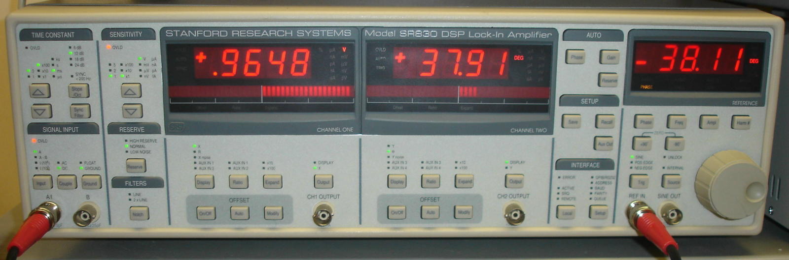
The photo above (hover to view full size) is a 'typical' lock-in amp, the model SR850 from Stanford Research. It includes a selectable transimpedance stage (current to voltage converter) at the input, and can measure down to nanovolts or femtoamps. It measures phase and amplitude, and is far beyond anything described here. The info I've included will allow you to build a basic analogue LIA, but if you need all the bells and whistles, you just have to buy the 'real thing'. Expect it to cost at least US$6k, and it will come with a serious learning curve.
Prior to the lock-in amplifier, an instrument known as a 'boxcar integrator' (aka boxcar averager) was used to achieve a similar result. The system used sampling that was locked to the signal frequency (and phase), then it took a short sample at a defined point on the waveform. For coherent waveforms (i.e. same frequency for the signal and reference), the average would not be affected by random/ non-coherent noise or interference. These also used very clever circuitry. They were first used in ca. 1950 (according to Wikipedia), so it's almost certain that the earliest versions would have used valves (vacuum tubes). I don't propose to cover these here, but there is quite a bit of info on-line (including a video of one in use).
In some respects, the boxcar integrator could do more than an LIA, but they have faded into obscurity for the most part. There are still devices that do the same thing, but they're more likely to be called a 'gated integrator' (e.g. SRS SR250). Units available today are not all-inclusive, so external metering and signal generation will probably be required.
Noise has always been the enemy of accurate measurements, and methods of minimising its impact will continue to be developed. Modern oscilloscopes with averaging can be considered (at least to an extent) a reasonable equivalent to the boxcar integrator, but they are still limited - at least for those models that remain affordable. As seen in Figs 0.2A and 0.2B, averaging does work fairly well, and it's certainly much simpler to set up than a boxcar integrator, or even a lock-in amplifier.
It should be noted that not all reference material describing lock-in amplifiers is completely reliable. To function, a lock-in amp needs the input and reference signals to be present for long enough for a decent average to be obtained. If the noise and signal levels are comparable (e.g. 100mV signal and ~100mV of noise after amplification) then the number of averages required may be reduced.
There's a great deal of literature available for anyone who wants to know more, but I suggest that you don't take everything you read as gospel. Like any other topic on the interwebs, some info is good and some is terrible. The following sites/ publications were used in the preparation of this article.
Note that some of the links may break without notice. I have PDF copies of some of those that are most likely to vanish (or lose their drawings as happens regularly with EDN).
Just for a laugh, I asked ChatCPT to tell me about lock-in amps. The result was less than ideal, with a fair bit of detail, but nothing actually useful. The result is (mostly) technically correct, but it's the sort of response you expect from a politician - lots of words that say very little. It's worth reading, if only to prove that AI isn't quite ready to take our jobs.
| Main Index Articles Index |