

|
| Elliott Sound Products | Instrumentation Amplifiers Vs. Opamps |
 Main Index Main Index
 Articles Index Articles Index
|
The term 'instrumentation amplifier' (aka INA or 'in-amp') is not always applied correctly, sometimes referring to the application rather than the architecture of the device. It used to be that any amplifier that was considered 'precision' (e.g. providing input offset correction) was considered an instrumentation amplifier, as it was designed for use for test and measurement systems. Instrumentation amplifiers are related to opamps, as they are based on the same basic (internal) building blocks.
However, an INA is a rather specialised device, and is generally designed for a specific function. They are not basic 'building blocks' that can be interchanged at will. INAs are not opamps, because they are designed for a rather different set of challenges. You can build an INA using opamps, or using a separate (including discrete component) front-end. Project 66 is a perfect example - it's a true INA, but in this case, specifically optimised for use with low level microphone inputs.
If you need particularly low and/or predictable DC offset performance, then it's better to use an off-the-shelf INA rather than try to make one using opamps or a discrete front-end. Because everything is in one package, thermal performance (in particular) is usually better than you'll ever get with a 'home made' solution. However, there's no reason not to use opamps for a roll-your-own INA, especially if the DC performance isn't critical. For audio applications, it's often easier (and significantly cheaper) to use opamps rather than a dedicated INA.
Instrumentation amplifiers are particularly useful when a very high CMRR ('common mode rejection ratio', sometimes shortened to 'common mode rejection' or 'CMR') is necessary. A common mode signal is one that appears on both input signal wires at the same voltage, and is most commonly noise picked up by long cable runs. There are other situations where CMRR is important too, especially in instrumentation systems, and this is where the name 'instrumentation amplifier' comes from.
An instrumentation amplifier is a purpose designed device, and unlike opamps there is no user accessible feedback terminal. The gain can be controlled by a single resistor, and the reference can be earth/ ground (as is normally the case), or some other voltage as required for your application. The specifications for INAs are usually quite different from those for opamps, because of the way they work.
There are some specs that are the same or similar as you'd expect to find with opamps, but others are quite specific to the INA. Supply voltages are commonly up to ±18V, and some can operate with only ±2.25V supplies [ 1 ], others up to ±25V [ 2 ]. Unlike opamps (which mostly have 'industry standard' pinouts for any given number of opamps in a package, typically 1-4), you cannot expect to find the same with INAs. Some will be the same as other similar devices, but many are not (even from the same supplier).
The general form of an INA is shown below. No values are given, because they vary from one device to the next. The feedback resistors are internal, and only one resistor is needed to set the gain. Some include an internal resistor to preset the maximum recommended gain - typically 100 (40dB) or 1,000 (60dB). Some INAs have offset null connections to allow the DC offset to be minimised, but others do not.
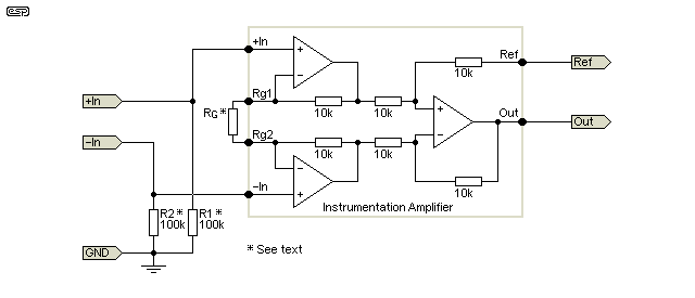
Figure 1 - General Form Of An Instrumentation Amplifier
Many INAs are specified for low or very low noise, but, like opamps, there are others that are more pedestrian. One area where most excel is common mode rejection, and this is the thing that sets an INA apart from a seemingly similar opamp circuit. This is not to say that equivalent performance can't be obtained from opamps, and as noted above this is often easier and cheaper. However, even the simplest INA made from opamps requires a dual device plus one other opamp (along with feedback resistors etc.), and the PCB real estate needed is far greater than a dedicated INA. Depending on the specifications you need for the application, prices range from under AU$5.00 to AU$50.00 each or more, so you need to select very carefully.
There are two main different configurations used for commercial INAs. One is as shown in Figure 1. INAs all have balanced inputs, but simply having a balanced input does not make a circuit into an INA. The balanced input stage is used internally with many INAs, so it has to be examined first.
A standard balanced input stage is shown below. While this is the basis of most (but not all) INAs, it is not an instrumentation amplifier in its own right. There are several well known and understood limitations of this circuit, with a major problem being its input impedance. R1 and R3 set the impedance, but R2 and R4 must be scaled accordingly to obtain the desired gain. For example, if you needed an input impedance of 100k and a gain of 10, R1, R3 would have to be 50k, and R2, R4 would then need to be 500k. This creates a large noise penalty. As shown, the gain is unity, and that applies whether the input is balanced or not. However, the gain for the positive input is unity only if the unused negative input is grounded.
Another problem is that the input impedances are not the same for each input. This isn't always an issue, but it's real and needs to be understood in the context of your requirements. Firstly, we'll assume a perfectly balanced ground referenced input, so the voltage applied to each input pin is exactly half the total (±500mV). The impedance of the positive input is clearly defined as being 20k, because it's made up by R1 and R2, which are effectively in series (ignore the input impedance of the opamp itself).
The negative input is another matter, because there is feedback around the opamp and applied to the opamp's -ve input pin. With the balanced input, the impedance seen at the inverting input by the source is 6.67k. This somewhat unlikely sounding figure is based on the voltage across R3. At the input end, it may have (say) 0.5V, but at the other (opamp inverting input) there's -250mV. The current through R3 is therefore not what you'd expect with 0.5V and 10k (500µA), but is 750µA, giving an apparent resistance of 6.67k.
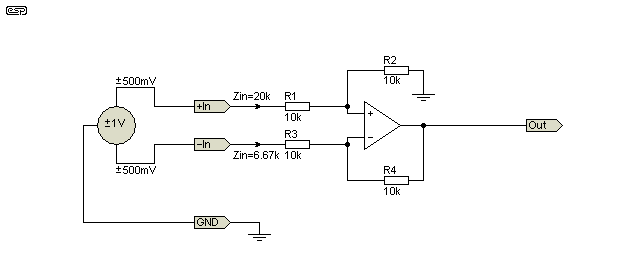
Figure 2 - Balanced Input Stage
If the source is fully floating (not ground referenced) such as a microphone capsule or other floating source, the impedance imbalance is of no consequence. The current into each input is the same, with (say) ±50µA flowing into each for the 1V source shown (50µA because the +In terminal has a 20k input impedance). The voltages measured at each input are radically different though, with the full 1V peak signal appearing at the +In terminal, and (close to) zero at the -In terminal (a few hundred microvolts is typical, opamp dependent). If you find this hard to grasp I can't blame you, as it initially seems to defy the laws of physics. I recommend that you build the circuit so you can verify that what I've claimed is, in fact, quite true.
The impedance at the +Ve input is 20k (as expected), but on the -Ve input it's almost zero (but only with a fully floating source). You'd expect it to be 10k (due to R3), but that isn't the case. Note that this anomalous situation can only occur when the source is fully balanced, having no ground reference. Balanced (floating source) input impedance is 20k, which is what you would hope for, but may not expect based on the voltages measured. Once the input source is ground referenced (e.g. a centre-tapped transformer or active balanced output circuit), the input impedances become 20k (+Ve input) and 6.67k (-Ve input, and still not as expected, but the reason is described above). These issues are fairly well known, but not always remembered when it's necessary to do so.
For common-mode (noise) signals, the impedances are balanced, despite everything seemingly indicating otherwise. This is the only thing that we are generally worried about when differential input amplifier circuits are used. The low output impedance of the balanced line driver swamps any variations that are seen at the inputs of the balanced input. However, CMRR reduces with increasing frequency, because the opamp has less open-loop gain at high frequencies (due to the internal compensation capacitor).
The impedance imbalance means that this circuit cannot be considered to be a 'true' INA. One of the requirements of an INA is that input impedances should be equal. While the circuit shown is useful, and it works well, never imagine that it can be used in place of the real thing. By all means use it for balanced microphone or line inputs, but not where any kind of precision is necessary. This is especially true for any application where the input impedances must be (close to) identical, or where good CMRR is needed at high frequencies. Be aware that even INAs will show degraded CMRR at high frequencies, because they also require internal compensation and they don't have 'infinite' bandwidth.
The next version is the same as the balanced input circuit described in Project 87. It's used in several commercial INAs, but there are a few limitations you need to be aware of. The main limit is minimum gain - unity gain is not possible. There is also a limit to the common mode voltage that can be accommodated. This requires explanation, but fortunately it's not as hard to understand as the Figure 2 stage.
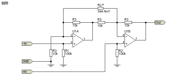
Figure 3 - 2-Opamp INA Circuit
This circuit is a 'true' INA in most respects, and although it is used in some commercial ICs it is a compromise. It has the advantage of using only two opamps (rather than three), but in terms of IC fabrication that's hardly a problem. RG can be included (or omitted), and if it's there it increases the gain. Using 10k for RG increases the gain to 4, and 1k increases it to 22. Unfortunately, if it's not included, the gain isn't unity - it's two. The gain cannot be reduced to unity without attenuating the inputs, which will impose a potentially serious noise penalty.
Av = 2 + ( 2 × R3 ) / RG Where Av is voltage gain, and R3 resistors are all equal
Of more concern is where you have a situation where there is a significant common mode signal. The first opamp has a gain of two, and that applies whether the signal is differential or common mode. If there is a 1V common mode signal (i.e. the same voltage applied to both inputs at once), the output of U1 will have a voltage of 2V. This isn't changed by R7 (if used), but it does mean that the maximum peak common mode voltage is somewhat less than half the supply voltage. This is not a problem for the most part, because high common mode voltages are uncommon in the 'real world' (especially for audio), but it's something you need to be aware of.
You also need to beware of high frequency noise. The two opamps act in series for common mode signals, so the small propagation delay reduces the available CMRR at high frequencies. No opamp (or any other circuit) is instantaneous, so the useful range may be severely limited if very fast opamps are not used. For example, with TL072 opamps (as an example only) CMRR at 50Hz might be around 63dB, it's reduced to only 37dB at 1kHz and a rather woeful 17dB at 10kHz. This isn't always a problem though.
Otherwise, the circuit is genuinely useful, and it works well - provided you don't need unity gain or extended response for common mode signals. The input impedance is high (set primarily by the input resistors R1 and R2), and common mode rejection is as good as the resistor tolerance used for the 10k resistors. I've shown 10k resistors for all values of R3, but they can be any suitable value that doesn't overload the opamps. If reduced to (say) 2.2k, resistor thermal noise is reduced. Naturally, higher values can be used, but they will increase the noise level.
This circuit works by subtracting the common mode signal from U1 with U2. If the signal is differential, the signal from U1 is added in U2, so a 1V input gives a 2V output. R7 increases the gain, but doesn't affect the CMRR. The gain equation isn't as straightforward as you might hope, because the circuit relies on several feedback paths.
The concept shown in Figure 1 is a 'real' INA in all respects. There are several benefits to this arrangement that are not available in the 2-opamp version. The input buffers can be operated at unity gain, giving the overall circuit unity gain as well. Gain is adjusted with a single resistor, and the gain formula is straightforward. However, you do need to know the values of R3 and R4, which are normally provided in the datasheet. They are nearly always all equal and commonly laser trimmed for high precision. Note that R6 is not connected to earth/ ground by default, but is designated 'Ref', because it's the reference pin. It is usually (but by no means always) connected to the earth or system common (zero volt) bus in the equipment. Note that the 'Ref' pin must be connected to a (very) low impedance or CMRR will be degraded. The impedance must be low for all frequencies of interest, including the common mode noise component.
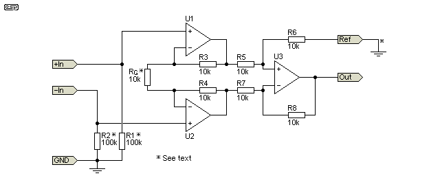
Figure 4 - 3-Opamp INA Circuit
Like the 2-opamp version, input impedance is set almost entirely by the external resistors. The CMRR of the circuit depends on the performance of U3 and the accuracy of R3-R8, assuming that U1 and U2 are (close to) identical which is usually the case. Because both inputs are subject to the same delay, use of slow opamps does not impair the performance. You can build this circuit using opamps, but it will take up a great deal more space than an INA chip. Unless the resistors are 0.1% or better, you won't get the performance of a dedicated IC.
Simulated using TL072 opamps, the Figure 4 circuit provides better than 85dB of CMRR at all frequencies up to 10kHz. A better opamp for U3 will extend this, as its performance at higher frequencies is the limiting factor.
The gain is set by RG, but you must know the value of R3 and R4 - these are normally provided in the datasheet. Assuming 10k as shown, the gain is determined by ...
Av = ( R3 × 2 ) / RG + 1 Where Av is voltage gain, R3, R4 are equal and R5 - R8 are equal
Av = 20k / 10k + 1 = 3
Different formulae may be provided in datasheets, but they will still give the same answer. In some cases in IC versions, R3 and R4 are equal, and R5-R8 are also equal, but a different value from R3 and R4. This doesn't change the gain equation, which relies only on the feedback resistors used on the input opamps.
The gain of the two input opamps is unity for common mode signals, regardless of the value of RG. It might not look that way at first, but remember that both opamps see the same signal (amplitude and polarity) for common mode inputs. RG therefore has no effect, as there is no voltage across it. When you examine specification sheets, you'll see that CMRR increases as the gain of the device is increased, because it's a ratio of the wanted (differential) signal to the unwanted (common mode) signal. If the wanted signal has more gain and the unwanted signal always has unity gain, the ratio between the two must increase.
Like many IC circuits, there are tricks and techniques that can be applied to improve performance. These can be critical to getting the results the application demands. It's only possible to cover a few of the more common (and/or useful) techniques, and datasheets and application notes for the selected device(s) are always a good place to start looking. It's common that you can often find just the solution you need in the datasheet for a related (but perhaps otherwise unsuitable) device, but fortunately most of the tricks will work with any device that uses a similar internal circuit.
Where common mode noise is a problem, sometimes it's worthwhile to use another opamp to drive the cable shield. Figure 5 shows an active shield driver that is configured to improve the CMRR by bootstrapping the capacitance of the input cable's shield, and thereby minimising any capacitance mismatch between the two inputs. A common mode mismatch will show up at the junction of the two gain resistors, and this is used to drive the input cable's shield.
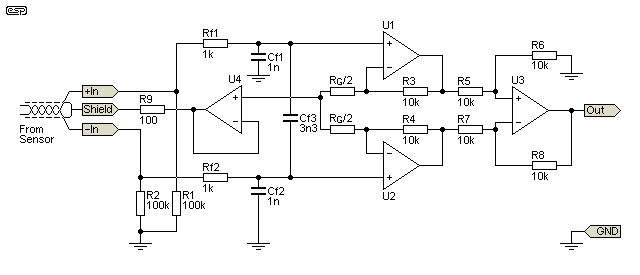
Figure 5 - Common-Mode Shield Driver Example
When techniques like this are used, it's important to test the circuit thoroughly, matching the 'real world' operating conditions as closely as possible. The above circuit also shows filtering resistors (Rf1 and Rf2) and capacitors (Cf1, Cf2 and Cf3), and Cf1, Cf2 need to be matched to maximise the common mode rejection. These parts should be carefully matched to within 1% or better if possible. Exact values are not important, it's only the difference between them that will cause a reduction of the CMRR. Cf3 doesn't need to be exact, as it's across the two inputs.
There will also be occasions where high voltage at the inputs are likely (or possible), so protection has to be added to ensure that the systems survives. Ideally, the system will be protected against any foreseeable 'event', but this is not always possible. In audio systems destructive events aren't common, but in an industrial setting all of that changes very quickly. It's not usually economically possible to protect against everything (a direct lightning strike for example), but a reasonable level of protection is always needed for anything that operates in a commercial or industrial environment.
Some INAs have protective diodes built into the chip, but if present they are usually limited to around 10mA or so. In most cases, diodes are connected to the supply pins, but this can easily give a false sense of security. If an external fault that delivers (say) +25V to the input(s) is diverted to a supply pin, it's quite possible that the ICs absolute maximum supply voltage may be exceeded. 99% of common regulators can only source current, so if something forces the supply rail to a higher than normal voltage, the regulator can't prevent it.
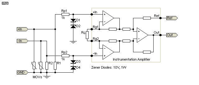
Figure 6 - Zener Diode Input Protection
A safer (but more expensive) option is to protect the inputs with back-to-back zener diodes. Using 10V 1W zeners means that the inputs can't be forced beyond ±10.6V, and the zeners can conduct up to 90mA continuously (depending on PCB heatsinking), and around 500mA for transient events. The zener circuits have to be protected against excess current, and the filter resistors (Rf1 and Rf2) shown above can also provide current limiting.
The 1k resistors shown would allow input voltages of up to ±100V for short periods, but the resistors have to be able to take the power (a little over 8W) for as long as is likely to be necessary in the application. This is completely dependent on the system itself, and the likelihood (or otherwise) of severe over-voltage. It's important that equipment is designed to suit the conditions. Trying to accommodate any possible fault condition is usually excessively costly, so the designer must be aware of probable (as opposed to possible) faults, and design for that.
In extreme cases, it might be necessary to use PTC (positive temperature coefficient) thermistors in place of (or in addition to) Rp1 and Rp2. Also known as 'Polyswitches', these will become high impedance if there's a fault, protecting the INA and the protective zeners. Care is needed to ensure that the zener junction capacitance doesn't cause problems such as reduced CMRR at high frequencies due to mismatched capacitance. It's likely that a circuit intended for harsh conditions may use both the filtering in Figure 5 and the protection shown above. In some cases even more protection may be needed before the circuitry shown. This might include MOVs (metal oxide varistors) as shown above, or 'Transorb' diodes, which are designed for very high peak currents.
The selection criteria for any and all protection circuits are application specific, and the designer is expected to know (or find out) the likely fault conditions for the equipment. It's beyond the scope of this article to provide any further details. It can be surprisingly easy to end up with protection systems that are more complex and/or costly than the circuitry it protects, but there's no choice if the equipment is required to be 'fault tolerant'.
CMRR is an important part of any INA, but it's not always necessary for it to apply at all frequencies. As noted above, the 2-opamp INA has rather poor CMRR at high frequencies, but if your application is DC (or very low frequency), this is not a limitation at all. The incoming signal leads can have a (relatively) vast amount of noise, but it can be filtered out so that only the DC component (and perhaps some low frequency noise) remains. Unlike the circuit shown in Figure 5, the tolerance of the filter capacitors isn't a major problem, because there is no need for good high frequency performance.
There are many applications where the system speed is such that no-one cares about high frequencies. A weighbridge (for example) doesn't have to work at high frequencies, and if it takes a couple of seconds before the reading is stable, that's usually preferred. For this type of application, a relatively slow response is essential to prevent the reading from moving around too much. Even 'lesser' applications (such as bathroom scales) usually have a fairly slow response so the reading doesn't jiggle around (essential when the display is digital, because you can't read rapidly changing digits easily - if at all).
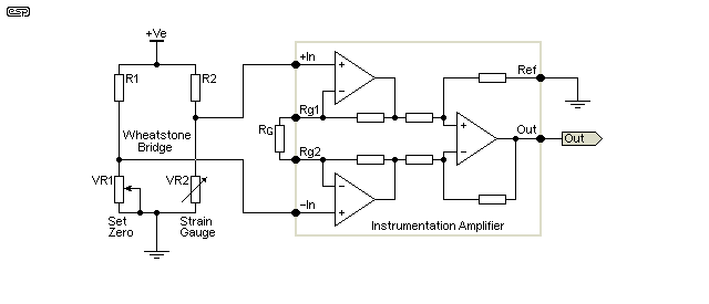
Figure 7 - Wheatstone Bridge Using A Strain Gauge
A very common use for INAs is for strain gauges. These can be part of anything from a weighbridge to 'bathroom' scales, and the only real variable is the sensitivity of the strain gauge. A detailed discussion of strain gauges is outside the scope of this article, but they are common in many weighing systems, for monitoring stresses in bridges or buildings and torque measurements for machinery.
The Wheatstone bridge is a very good example of a system where there is a large common mode signal, and INAs are ideal candidates to measure the small variation of resistance while a comparatively large DC offset is present. The strain gauge changes its resistance ever so slightly when it's under stress, and the INA is used to detect the resistance change. However, it must ignore the common mode signal, and react only to the differential component created by the Wheatstone bridge. VR1 is used to balance the bridge when there is no strain applied to the gauge. Values have not been shown because of the wide variability of static resistance for strain gauges, which may be anything from a few ohms up to 10k or more. Note that no temperature compensation is shown, but it's usually essential.
A typical 'load cell' (a strain gauge in a specially designed housing to monitor force/ weight) may only provide an output of 2mV at full load with an excitation voltage of 10V. Although only a single strain gauge is shown in Figure 7, it's common to use at least two and sometimes four, with strain gauges for all four sections of the Wheatstone bridge. This requires that two will be in compression and two in tension, and the output is increased by a factor of 4 times. In this case, the 4 strain gauges form the Wheatstone bridge, so there are no other parts. These are usually (but not always) temperature compensated because all 4 sections of the bridge are matched, and at the same temperature.
As this article has (hopefully) demonstrated, the instrumentation amplifier is a specialised device, and is particularly suited to situations where there is (or may be) a significant common mode voltage along with the desired signal. INAs are also used as microphone preamps, and basically can be used anywhere that requires good common mode rejection. The choice of INA is critical for applications where there may be high frequency common mode noise. Not all are effective across the audio band, so it's essential that you look at the datasheet closely before making a decision.
The specs can be a little daunting for the uninitiated, but once you are acquainted with some of the terms and how they apply you'll be able to work through them easily enough. It can be helpful to search for a device that is specifically designed for your application. It's unrealistic to expect that there will be an INA that's an exact fit for everything, but you can get something that suits your needs once you understand the devices well, and know how they can be adapted.
One thing that can be very important is the earthing (grounding) scheme used in an application. Improper earthing arrangements can cause serious errors, so PCB layout is often very important. This is especially true when very small signal levels are available, and high gain is needed to bring the signal to a level that can be used by the following circuits. Datasheets and application notes are essential reading if high accuracy is needed.
There are several INAs that are not designed specifically for instrumentation, but are optimised for very low noise. These can have different titles, but there are some that are described as 'self contained audio preamps' or similar. These don't use opamp based front-ends, and are intended for microphone preamps and other low-level preamps, with the emphasis on audio rather than instrumentation. I haven't listed them here, and some are now classified as obsolete so you wouldn't be able to get one even if you wanted to.
1 INA128 Datasheet (3-opamp INA)
2 INA126 Datasheet ('Micropower' 2-opamp INA)
3 INA103 Datasheet (Very low noise 3-opamp INA)
4 AD623 Datasheet (Low power, low voltage 3-opamp INA)
5 What's The Difference Between Operational Amplifiers And Instrumentation Amplifiers? - Kevin Tretter (Electronic Design)
6 Measuring Strain with Strain Gauges - National Instruments
7 A Designer's Guide to Instrumentation Amplifiers, 3RD Edition, 2006 - Analog Devices
8 INA217 Datasheet (3-opamp INA)
 Main Index Main Index
 Articles Index Articles Index
|