

|
| Elliott Sound Products | Compound Vs. Darlington |
 Main Index
 Articles Index
There are many reasons that designers need very high gain transistors, and although they are available in a single package, it is generally better to build your own using discrete devices. This gives much greater flexibility, and allows you to create configurations that are optimised for the specific task required.
To create a high gain transistor, it is a matter of connecting two or more transistors such that the collector current of the first is amplified by the second. Thus, if two devices have a current gain (β or hFE) of 100, the two devices connected together can give an overall current gain of as much as 10,000 - this will be looked at in greater detail later.
For a variety of reasons, current gains of more than 2,000 or thereabouts are rarely achieved in practice, but a β of well over 1,000 is easily achieved - even for high current configurations. These discrete compounded transistors are found in power supply and power amplifier designs, as solenoid drivers and general purpose high current switches or other linear applications.
For many applications, I have always considered the Sziklai (aka 'compound') pair as the preferred option, but both that and the Darlington pair are essential to the development of modern linear ICs, power supplies and power amplifiers (to name but three applications). Although the Darlington pair was discovered/ invented first, in this article, I shall break with tradition and place the less well known configuration first in all diagrams. I do this because it is a better arrangement IMO, having greater linearity (less distortion if used for audio), and far greater thermal stability than the older and better known Darlington Pair. The configuration I refer to is called a Sziklai [ 1 ] or compound pair, and this combination has also been referred to in the past as a 'Super Transistor'. The differences between the two different topologies are often rather subtle, but in many applications the compound pair gives better performance.
The Darlington pair was invented in 1953 by Sidney Darlington (1906 – 1997). The Sziklai pair was invented by George Sziklai, a Hungarian engineer who emigrated to the US (1909 - 1998). Note that there are also Darlington and Sziklai triples - three transistors. A Darlington triple is simple, but there are several different ways that a Sziklai triple can be implemented.
The compound/ Sziklai pair is a configuration of two bipolar transistors of opposite polarities, so will always consist of one NPN and one PNP transistor. The configuration is named after its Hungarian born inventor, George Sziklai. It is also sometimes known as a CFP (complementary feedback pair). The composite device takes the polarity of the driver transistor, so if a compound pair is made with an NPN driver and PNP output device, the overall device behaves like an NPN transistor. This will become clearer as we progress.
A Darlington pair always consists of two transistors of the same polarity. An NPN Darlington will have two NPN transistors connected as shown below, and a PNP device will use two PNP transistors. The Darlington configuration was invented by Bell Laboratories engineer Sidney Darlington in 1953. He patented the idea of having two or three transistors on a single chip, sharing a collector.
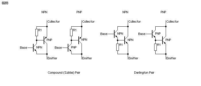
Figure 1 - Basic Configurations Of Devices
As you can see from the above, the compound pair polarity is determined by the driver transistor, so an NPN driver with PNP output transistor behaves like an NPN transistor and vice versa. It is a little disconcerting to see that the emitter of the power transistor is really the collector of the compound pair, and this subtle distinction has trapped a few designers over the years. Although it is not immediately obvious, the gain of the two different topologies is slightly different, because the compound pair has a small amount of in-built negative feedback which reduces the gain.
For the sake of convenience, let's assume that the driver transistors in both configurations have a gain (β) of 10, and the output transistors have a gain of 5. For the compound pair, 1mA of base current will cause 10mA of collector current in Q1, and (ignoring the resistor R1), this will provide 10mA base current to Q2. This will become 50mA collector current for Q2. The total overall collector current is 60mA, and the emitter current is 66mA (it includes the base current of Q1).
Looking at the Darlington pair, with 1mA of base current into Q1, the collector current of Q1 is 10mA, and the base current for Q2 is 11mA, because the base current is included in the current flowing from the emitter. Collector current of Q2 is therefore 55mA, and the total collector current is the sum of both transistors (the collectors are tied together). Collector current is therefore 65m and emitter current is 66mA (Q1's base current is added).
Therefore, the β (aka hFE) of the compound pair is 60 and that of the Darlington pair is 65. This relationship is maintained regardless of the actual gains of the two transistors (remember that gains of 10 and 5 were used for convenience only). Note that when R1 is included the results will be different, and 'real world' parameter spread means that measured results will be very different from the value calculated. The actual formulae are ...
Compound Pair β = βQ1 × βQ2 + βQ1
Darlington Pair β = βQ1 × βQ2 + βQ1 + βQ2
The small gain difference is immaterial and normal component variations will be far more significant. Likewise, a temperature change of only a few degrees will completely override any measurable gain difference. For all practical purposes, the total gain for either configuration is approximately ...
β = βQ1 × βQ2
To obtain the maximum possible gain it's important to ensure that the driver transistor for either circuit has enough collector current to ensure acceptable hFE. When run at very low collector current, most transistors will have a gain that's well below the quoted figure in the datasheet. For example, a BC549 has a 'typical' gain of 520 at 2mA, but this falls to 270 at 10µA. It falls further as collector current is reduced below 10µA. The base-emitter resistor (R1, shown in each of the configurations in Figure 1) should be sized to ensure that the drive transistor has a collector current that's above the minimum. The resistor also helps to ensure a faster turn-off and minimises leakage current.
For example, assume that Q1 and Q2 have a gain of 500 at currents above 100µA. If Q2 has a collector current of 10mA, its base current will be around 20µA. To ensure Q1's gain is acceptable, it needs to operate at a current of at least 100µA. R1 is therefore required to pass around 80µA, so needs to be about 8.2k (assuming 0.7V base-emitter voltage). This is just Ohm's law, and can be calculated for any combination of device gains for Q1 and Q2, whether wired as a Darlington or Sziklai pair.
Apart from the negligible gain reduction, the only real disadvantage of the compound pair configuration over the Darlington Pair is the saturation voltage. This is important for high current switching applications, because a higher saturation voltage means a greater thermal dissipation. This can make the difference between needing a heatsink or not, or needing a bigger heatsink that would otherwise be necessary. There are many different ways around this problem of course, but such a discussion is outside the scope of this article.
 | Note that for all the following examples, generic transistors from the SIMetrix [ 2 ] simulator are used. NPN devices are 2N2222 and PNP are 2N2904. These are both nominally rated for around 625mW dissipation and have a claimed minimum gain of 100, although this varies widely (as do all transistors) and is dependent on temperature and current. |
The compound pair has a slightly higher saturation voltage than a Darlington pair, as shown in Figure 2. This is actually somewhat counter-intuitive, and you may find descriptions that claim that the opposite is true. The difference is not great - 765mV for the Darlington pair and 931mV for the compound pair as shown below, but that's enough to make a significant difference in a high current switch. The input signal is a pulse waveform, with a minimum value of 0V and a maximum of 12V. Base current is therefore around 1.14mA for the compound pair, and 1.05mA for the Darlington. The reason for the small difference is explained below.
In the case above, the power dissipation in the compound pair is 52mW and 44mW for the Darlington. The difference is trivial here, but becomes much more important as current increases. When the current is 10 times or 100 times as great as the ~120mA used in this example it is easy to see that the dissipation will become very high. To a significant extent, this is no longer a problem in modern high current switches, because MOSFETs or IGBTs (insulated gate bipolar transistors) are now used for most serious switching applications.
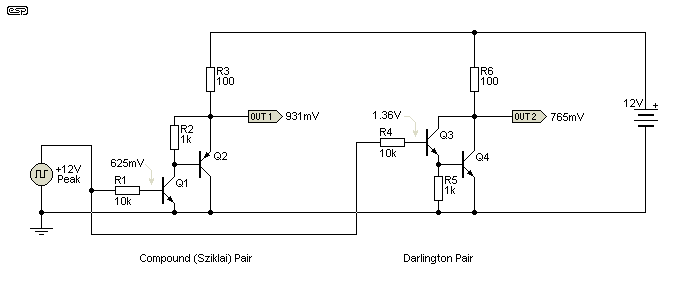
Figure 2 - Switching Saturation Voltage Test
One area where the compound pair wins easily is the required turn-on voltage. The compound pair needs only 625mV vs. 1.36V for the Darlington pair (this is subtracted from the base supply voltage to calculate the current through the 10k base resistors). Again, this might not seem significant, but there will always be applications in electronics where a low turn-on voltage is advantageous because of other circuit constraints. While this is rarely a major issue with modern switching systems, it influenced many earlier designs before MOSFETs and IGBTs were available. The Sziklai pair (as simulated) has a slightly greater turn-off time than the equivalent Darlington (1.2µs vs. 805ns respectively), and while this is rarely an issue in low-level circuits, it becomes important for high speed power circuits. Switching times can be reduced dramatically by using a lower base drive resistor (and a corresponding reduced drive voltage).
So far there is really not much between the two circuits, but it seems that overall the Darlington has a slight advantage. For this reason, Darlington connected transistors are still the most common for any form of switching that does not warrant the use of MOSFETs or IGBTs. It is a very useful circuit, and there are many integrated Darlington transistors available (the TIP141/ 146 NPN/ PNP respectively, 80V maximum) are probably the best known examples). As always, the most appropriate topology has to be chosen to suit the application, and there is no single 'best' way to perform the various tasks needed in electronic circuitry.
Both Darlington and Sziklai pairs are used in linear circuits, and overall Darlington pairs are the most common. Readers of The Audio Pages will have noticed that almost without exception, I have used complementary pairs for power amplifier output stages. This is a relatively uncommon approach, but there are good reasons for this choice. I used the complementary output stage in the second amplifier I ever designed, and have continued to use it ever since.
It was determined and demonstrated long ago [3, 4, 5] that the compound pair has greater linearity than the Darlington pair, and although this information seems to have been ignored by most people for a very long time, it is still true. One of the interesting things about facts is that they don't go away, even if ignored. 
Figure 3 shows a pair of simple emitter followers, one using the compound pair and the other a Darlington. This is a fairly easy job for any transistor circuit, and one would not expect a significant difference in a circuit that has almost 100% degenerative feedback. The input signal is a 1V peak (707mV RMS) sinewave, with a 6V DC bias to place the output voltage at the approximate half-supply voltage.
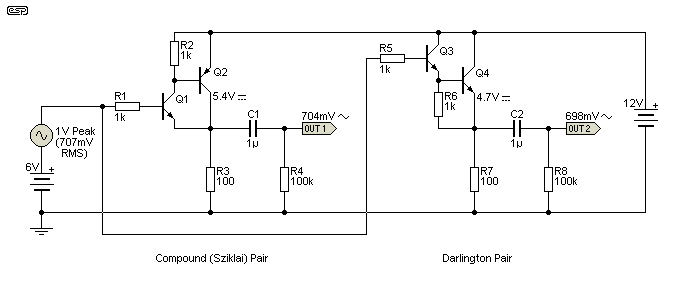
Figure 3 - Compound And Darlington Emitter Followers
The first thing you notice is that the compound pair has a higher output voltage - it's 99.5% of the input voltage, vs. the Darlington pair which only manages 98.7%. Admittedly, this is hardly a vast difference, but it is notable nonetheless.
Of more interest is the distortion contributed by the two configurations, and this is demonstrated below. Quite obviously, the compound pair (green trace) has fewer harmonics above the -120dB noise floor, and they are all at a lower level - by 20dB or more!
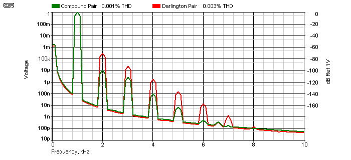
Figure 4 - Distortion Performance of Compound And Darlington Emitter Followers
A FFT (Fast Fourier Transform) of the output waveform lets us see the harmonic structure of the signal. Simulators have a real advantage here because they can generate perfect waveforms (zero distortion) and have infinite dynamic range. Any harmonic that's more than 120dB below the fundamental is not only buried in the noise floor of even 24-bit digital systems, but is well below audibility for any system.
The THD (Total Harmonic Distortion) figures are a good indicator of linearity. A perfect system contributes no distortion at all. As you can see, the Darlington pair has 3 times as much distortion as the compound pair. Both figures are excellent and are well below audibility, but remember that every stage of a system contributes some distortion, so keeping overall linearity as high as possible is important.
As I have noted in many of the articles on this site, I consider the THD of an amplifier to be an important measurement, not necessarily because we can hear low levels of distortion, but because it gives a good indication of overall linearity. Any non-linearity causes intermodulation distortion (IMD), and it is IMD that is almost always considered the most objectionable.
The so-called TID (Transient Intermodulation Distortion) is largely a crock - there is no evidence whatsoever that any competent amplifier fed with real music signals generates TID. This was probably one of the most elaborate hoaxes that the audio community has seen so far, largely because it was widely reported and came from seemingly credible audio designers. The fact is that TID is real, but only if the amplifier is subjected to test signals that never occur in any recorded or live programme material.
If the Darlington and Sziklai circuits are extended to triples, a Darlington must (by definition) use three transistors of the same polarity. For the Sziklai (and for NPN), you can have an NPN first stage followed by a PNP Darlington, or an NPN, PNP, NPN combination. Remember that the Sziklai arrangement assumes the polarity of the input transistor. You could also use an NPN Darlington followed by a PNP, but you lose the advantage of a single base-emitter junction. I don't propose to cover these alternate combinations in any further detail, but feel free to experiment, either on the workbench or using a simulator.
I did run a few simulations though, and an NPN, PNP, NPN Sziklai triple outperformed any other configuration (including Darlington) by a wide margin. However, you would need to be very careful to ensure than an amplifier using this arrangement remains stable, as the overall phase margin of the amp as a whole may be affected to the point where it oscillates. Extra compensation may be required. These are things that always need to be considered when designing linear circuits that use feedback. The Darlington triple has a relatively benign phase shift (simulated using the same transistor types [e.g. BCxxx, BDxxx or TIPxxxx] for all tests).
In some classes of electronic equipment, thermal stability never needs to be considered. There are many designs where even quite radical changes to base-emitter voltages (for example) are simply and easily compensated by a feedback network, so never cause a problem. Of course, this assumes that adequate heatsinking is provided so that transistors remain within their safe operating areas.
For other designs such as push-pull power amplifiers, thermal stability is paramount. Depending on the design and the designer, the thermal feedback circuit can be quite complex and hard to get exactly right, although it usually looks quite simple in the schematic. The phenomenon of thermal runaway is invariably caused by insufficient attention to the thermal characteristics of the output stage. For many industrial applications this is easily solved by operating the output stage with no bias at all, thus preventing any possible issues.
However, this is usually not feasible in an audio circuit, because zero bias output stages cause crossover distortion (sometimes called 'notch' distortion). This is very audible - especially with low level signals - and was part of the reason that many transistor amps got a bad name when they were first released into the market. They might have measured better than their valve counterparts, but only because the measurement was not done correctly at the time, or the person taking the measurement failed to notice where the problem(s) lay. A great many people hated the sound of many early transistor amps, but it took a while before the reason was understood.

Figure 5 - Bias Stability Test Circuits
A transistor's gain varies with temperature, and when the temperature increases, so too does the gain. This temperature dependency is maintained up to temperatures that will cause device failure. In addition, the base-emitter voltage decreases by approximately 2mV / °C, so some means of stabilising bias current is mandatory.
In a compound pair, the influence of the output device is considerably less than that of the driver. There is some effect as the output transistor gets hotter, but it is considerably smaller. The primary device that determines the bias current is the driver transistor, and it is much easier to maintain a reasonably constant temperature for a transistor that dissipates comparatively little power. The overall thermal sensitivity of the compound pair is significantly better than that for a Darlington pair, and the power transistor sensitivity is far lower.
In contrast, a Darlington device is highly dependent on the base-emitter voltage of two cascaded junctions, so the effect is doubled. If both the driver and power transistor get hot, the current increases markedly, and is much harder to control. This is compounded by the fact that most amplifiers using a Darlington output stage have the driver and power transistors mounted on the same heatsink, along with the bias servo transistor. In general, this is may be a mistake regardless of output stage topology as shown below.
| Transistor Temperature | Compound Pair | Darlington Pair | |
| Q1, Q3 (Driver) | Q2, Q4 (Output) | Total Current | Total Current |
| 25 °C | 25 °C | 41 mA | 41 mA |
| 75 °C | 25 °C | 123 mA | 96 mA |
| 25 °C | 75 °C | 44 mA | 87 mA |
| 75 °C | 75 °C | 126 mA | 148 mA |
The temperature dependence of the two circuits in Figure 5 is shown in Table 1. Because it is much easier to keep the driver transistors at a consistent temperature, it is apparent that it will be far easier to maintain a stable bias current using the compound pair than can ever be the case with a Darlington pair. This has been proven in practice - none of my original designs presented on this website has an issue with thermal stability, and all bipolar designs use the compound pair output stage. The bias servo transistor must be in thermal contact with the driver transistor(s) in a compound pair output stage. Deciding on the optimum location is harder when a Darlington output stage is used. Because there is always considerable thermal lag between the die and heatsink temperatures, placing the bias servo on the heatsink is not as effective as it should be (at least in the short term).
 | Note that the figures shown in the table show far less variation that you will experience in a typical power amplifier. This is because of the 1 ohm emitter resistors, which provide a far greater stabilising influence than the more common 0.1 or 0.22 ohm resistors typically used. The 1 ohm resistors were used for consistency and convenience for the purposes of explanation, and were not selected to be specifically representative of reality. There are too many variables in a real amplifier, so the idea was to show the trend, not absolute values. |
There have been (spurious and mostly nonsensical in my opinion) claims that thermal effects cause distortion in amplifiers and output stages [ 6 ]. While this does appear to have some effect in an integrated amplifier (power 'opamp' ICs for example), it should be negligible in any discrete power stage, and is likely to remain well below audibility in any design. Assuming that there is some substance to the claims as applied to discrete designs, it is likely that there will be smaller and less problematic thermal variations in the driver stages than the output devices. In general, I consider claims about thermal distortion to be 99% complete nonsense, and contrary to the reference noted above, explain nothing of any real importance.
Because of the known problems with thermal stability, some manufacturers have released power transistors with integral (but isolated) diodes to form part of the bias stabilisation network when the transistors are used. Personally, I think this is a stupid idea - the constructor ends up with a completely non-standard transistor, and when (not if!) it becomes discontinued there will be no replacement and an entire amplifier may have to be scrapped if a power transistor fails and a (genuine) replacement device can't be located. The alternative is a re-design, which may not be possible (depending on PCB layout, etc.).
In the early days of silicon transistors it was difficult to make decent PNP power transistors, so the compound pair was used in a great many amplifier output stages, leading to the then common 'quasi-complementary symmetry' output stage. One of the early amp designs described in the ESP projects section uses this output stage [ 7 ]. Over the years, there have been many schemes to improve on the basic quasi-complementary stage, but in reality nothing really needs to be done.
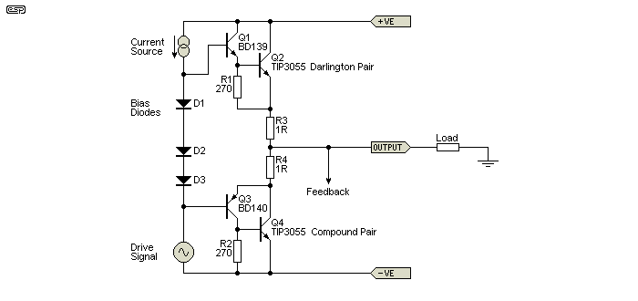
Figure 6 - Quasi Complimentary Symmetry Output Stage
At various stages, various people have added diodes to the compound pair so both sides of the push-pull stage have the same bias voltage and turn on in a more similar manner. While this can make a big difference, these days it's not worth the effort. Some attempts to 'improve' the circuit only managed to make it worse. These days, almost no-one makes quasi complementary symmetry amps because excellent NPN and PNP pairs are now readily available and it would be silly not to make an amplifier that's fully complementary symmetry.
The scheme has been described in some detail here because it is an important milestone in the evolution of modern amplifiers, not because it is currently suggested for a new design. Having said that, there are undoubtedly situations that could arise that make the general scheme potentially useful. For this reason alone, it is worth remembering - one never knows when such information will come in handy.
The three common power output stages are shown in Figure 7. There are obviously others, but they are generally based on one or another of the above. To make things more interesting, there are also variations that use a combination of compound pair and Darlington configurations, but these will not be covered here.
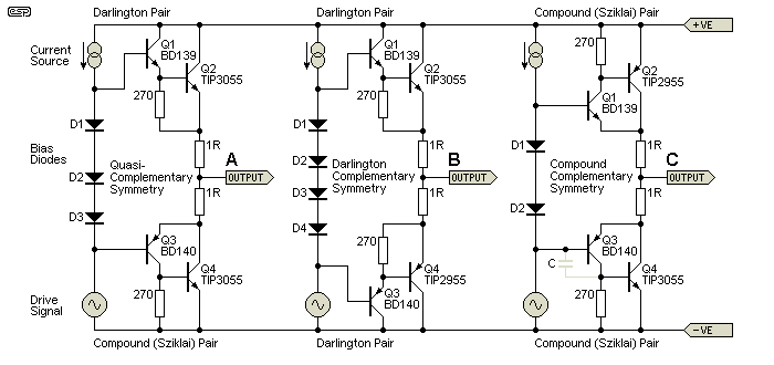
Figure 7 - Three Common Output Stages
The oldest of the three is A, the quasi-complementary symmetry stage. As noted above, this was common before true complements to high-power NPN transistors existed. Once at least passable PNP power devices were available (albeit at higher cost), full complementary symmetry (B) using Darlington pairs became common. This type of output stage has remained the most common for many, many years. When appropriately biased, all these stages have fairly good distortion performance, with the Sziklai pair being the best, and quasi-complementary the worst. With the exact circuits shown above, all have less than 1% THD when loaded with 8 ohms. (Sziklai, 0.05%, Darlington - 0.23%, Quasi-complementary - 0.65%, noting that these results were simulated.)
The least common is that shown in C - full complementary symmetry using compound pairs. I saw this used first in a little 30W(?) amplifier that if I recall correctly (and it's entirely possible that I don't) was one designed by Sir Clive Sinclair [ 8 ] in the early 1970s, and thought it was extremely clever. Try as I might, I've never been able to find the schematic on-line though. I promptly built an amp to test the output stage, and was pleasantly surprised in all respects. With few exceptions, every bipolar output amp I have designed since then has used this configuration, because I found its linearity and thermal stability to be markedly superior to the traditional Darlington stage.
For reasons that I have always found obscure and somewhat mysterious, I've found that every amp I've designed using this configuration has parasitic oscillations on the negative half, and the addition of a small capacitor has been necessary every time. Strangely, I've never had an issue with parasitic oscillation with quasi-complementary amps (although many years have passed since I built one), even though the negative side uses an identical compound pair. It makes no difference which side is driven (NPN or PNP voltage amplifier transistor) and which has the current source, and nor does it matter if the current source is active or bootstrapped. Only the negative side ever shows any sign of parasitic instability, and a small cap (typically 220pF) installed as shown stops it completely.
The final configuration is a fairly clever modification of the compound pair. Personally (and the obvious cleverness notwithstanding), I consider it an abomination - it has high distortion, extreme thermal sensitivity and very poor transient overload recovery characteristics. Despite this, there have been some commercial amps using the circuit shown, and there are even some who consider the sound to be 'better' than conventional output stages. This is not an argument I will entertain.
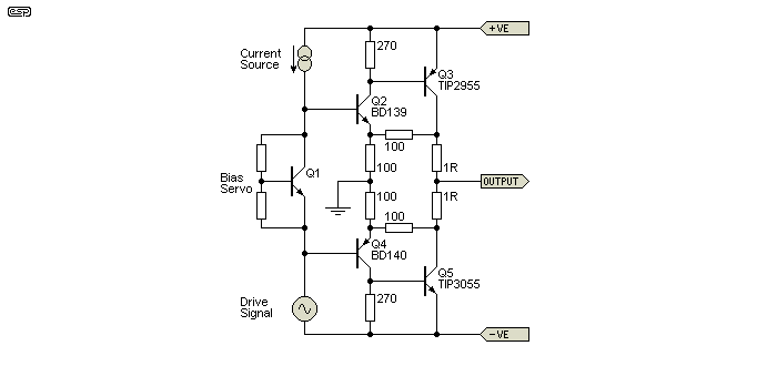
Figure 8 - Output Stage With Gain
As shown above, the output stage has a nominal gain of about 2, based on the 100 ohm resistors from the output to the driver emitters and then to earth. In reality, gain will be considerably less, because the stage has a relatively high output impedance (it's around 4 ohms as shown). This is in contrast to the other configurations shown above, which all have a low output impedance - typically 1 ohm as set by the emitter resistors in these examples.
Thermal stability of these stages is always a nightmare - I've only ever worked on a couple (and built one to test the idea many, many years ago), and found all of them to be highly thermally unstable. It is possible to design a bias servo (based on Q1) that will keep the stage from thermal runaway, but it's by no means easy to do, and the results are never completely satisfactory. Quiescent current typically varies by up to three times the nominal, and sometimes seems to have a mind of its own. Excellent heatsinking is mandatory!
Unlike the complementary symmetry stages (including quasi-complementary), open loop distortion performance is dreadful. Even operating at low gain as shown, distortion is close to 4% with over 150mA of output device quiescent current, almost 5 times as great as that from a Darlington pair output stage with roughly similar output stage bias current. If readers have twigged that I'm not fond of this arrangement then I've done my job. 
It's also worth noting the worst case dissipation in the 100 ohm resistors to earth (or other value as determined by the design). It can be a great deal higher than expected - in the case of the amp shown and with ±25V supplies, these resistors can dissipate over 3W each if the amp is driven into hard clipping. Under normal operation with music, dissipation is usually minimal. This is a design that requires extraordinary care in design, because there are so many things to get wrong.
However, like everything else in electronics, it may be ideal for some obscure application. Because of the gain structure, it is capable of fully saturating the output transistors in clipping. This means that if you happen to need a full level (rail to rail) squarewave output but also require the amp to be capable of linear operation, then this is the ideal circuit. I have found one (and only ever one) application for this for a client project, and in this rather odd role it performs perfectly.
There is only one instance on the ESP site where a compound pair is used for low level amplification, and that's for a microphone preamp [ 9 ]. Figure 8 shows two highly simplified versions, one using compound pairs and the other using Darlington pairs for comparison. The complete circuit is a long-tailed pair in both cases, and one might expect that the two versions would have roughly similar performance.
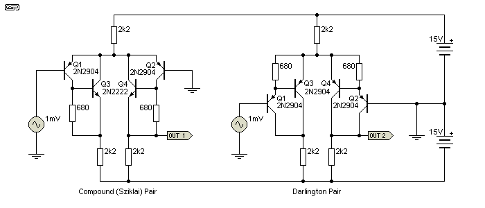
Figure 9 - Long-Tailed Pair Circuits
This is an area where the term 'super transistor' really comes into its own, because the compound pair version shown above has almost 10 times as much gain in an otherwise identical circuit using Darlington pairs (the voltage gain is 832 vs. 86). With an output of 832mV (compound/ Sziklai) and 86mV (Darlington), the distortion is around 0.06% for the Sziklai pair, and 0.04% for the Darlington. If the output of the Darlington stage is increased to the same as that from the Sziklai pair, its distortion doubles. IMO, there is no comparison - the Sziklai pair is the winner on all counts.
In all cases, the gain is affected by the emitter current of the transistors. Remember that internal emitter resistance (re ['little' re]) is roughly determined by the relationship re = 26 / Ie (in milliamps). This internal resistance means that at very low current, the internal emitter resistance is high, so circuit gain is reduced. This characteristic is used to create VCAa (voltage controlled amplifiers), so it's a balancing act to get the right transistor combinations with the right emitter current to get the highest performance. This becomes tricky when you have two transistors (either complementary or Darlington), as they draw very different currents.
In reality, there are not many requirements for the high gain and linearity of the compound pair in discrete circuits, but it is extremely common in ICs, where it is still difficult to fabricate high performance PNP transistors on the silicon substrate. Accordingly, many of the PNP transistors are actually compound (Sziklai) pairs in a great many opamp IC circuits. This is especially true for 'power opamps' - IC power amplifiers.
A common comment of mine is that all electronics devices are made from compromises, and the circuits described here are just that. The Darlington pair is a very popular topology, and there are many transistors that are in fact a basic integrated circuit - this is certainly the case with Darlington transistors. Built into the standard 3-lead package are two transistors, one or two resistors and sometimes a power diode as well.
As far as I'm aware, no-one has ever integrated a compound pair as a single transistor. I don't know why it's not been done, but there probably isn't much point. The compound pair works best when the driver is thermally separated from the power transistor, and this cannot be done if the two are on the same piece of silicon (or even just in the same encapsulation).
As far as making audio power amplifiers is concerned, both configurations work very well if properly designed, and there is no reason to believe that there will be any audible difference in a properly conducted double-blind test. It goes without saying that non-blind tests have consistently 'proven' that one or the other configuration is 'better' - which one depends entirely on the prejudices of the listener(s).
Many highly acclaimed amps have been made using both topologies, so audibility claims are obviously frivolous at best.
It is hoped that this article has provided some additional (and useful) information for anyone wanting to know more about these popular circuits. It's fair to say that without both the Darlington and compound/ Sziklai pair, the proliferation of high quality transistor power amplifiers would have been severely curtailed.
1 - Sziklai Pair - Wikipedia, the free encyclopedia
2 - Analogue Circuit Simulation Software from SIMetrix Technologies
3 - The Audio Power Interface, Douglas Self, Electronics World September 1997, p717
4 - Power Amplifier Design Guidelines - Output Stages, Rod Elliott
5 - Intermodulation at the amplifier-loudspeaker interface, Matti Otala and Jorma Lammasneimi, Wireless World, December 1980, p42
6 - Memory Distortion - Part 1 : Theory
7 - Project 12A - El-Cheapo, presented in more or less original form
8 - Clive Sinclair (Wikipedia)
9 - Project 66 - Low Noise Balanced Mic Preamp, Phil Allison & Rod Elliott
 Main Index
 Articles Index