
|
| Elliott Sound Products | CFB Vs. VFB |
 Main IndexArticles Index
The vast majority of common opamps and power amps use voltage feedback. Current feedback used to be common for early power amps (most often using a single supply), and was also used in valve (vacuum tube) power amplifiers. In this article, we'll look at the differences, which in many cases are surprisingly subtle. Despite the term 'current feedback' there is always a voltage present at the feedback node, and a number of writers on the topic have disputed the term 'current feedback'. In most cases they're wrong, and current feedback opamps (while uncommon) offer some significant advantages.
Current feedback also offers some benefits with power amplifiers as well. However, one thing that CFB amplifiers are not designed for is high DC accuracy. This is rarely a major problem in the applications where CFB opamps are used, but there's a significant disadvantage with an audio power amplifier, one of the main reasons they fell from favour. Almost all CFB power amps use capacitor coupling from the amp to the load (the speaker), because it's hard to minimise the DC offset.
It's important to understand that there are two completely different definitions for current feedback. The first is where the amp is designed to provide a constant current through the load (a trans-impedance amplifier), or uses a mixture of voltage and current feedback to obtain a specified output impedance that's significantly greater than the 'ideal' zero ohms. The Project 27 guitar amplifier is a case in point, where the output impedance is deliberately raised to allow the speaker to 'do it's own thing' as is expected for a guitar amp. Current drive in this form is also used with reverb tanks, and many other inductive transducers.
The second definition is applicable to Project 37 (DoZ Preamp) and Project 217 'practice' amplifier. In these cases, the feedback is applied as a current into a low-impedance inverting input. Unlike a VFB amplifier which has a pair of high-impedance inputs, in a CFB circuit the inverting and non-inverting inputs have very different input impedances.
The CFB amplifier (or opamp) sacrifices DC offset performance for wide bandwidth and (usually) a much greater phase margin when feedback is applied. The bandwidth of a CFB amplifier is determined by the ft of the transistors (and perhaps a Miller [dominant pole] capacitor), but the design means that the resistance of the feedback resistor is the dominant influence. The feedback resistance is almost always a comparatively low value. Unlike a VFB circuit, using equal value resistors for the two inputs does not improve the DC offset, but makes it worse!
A great deal of the literature you'll find for CFB amps and opamps concentrates on advanced maths, and tends to be analytical, rather than simple explanations for the internal processes. A perfect example follows, including 'equivalent circuits' that are (IMO) not very helpful for beginners, and aren't even much use for anyone other than an academic in the field. That doesn't describe me, and I doubt it describes many of my readers either.
The following is a quote from the TI application Report [ 1 ] ...
The ideal VFB opamp model is a powerful tool that aids in understanding basic VFB opamp operation. There is also an ideal model for the CFB opamp. Figure 1A shows the VFB ideal model and Figure 1B shows the CFB ideal model.

Figure 1.1 - Voltage Feedback vs. Current Feedback Ideal Models
In a VFB opamp ...
Vo = a × Ve
Where [ Ve = Vp - Vn ] is called the error voltage and [ a ] is the open loop voltage gain of the amplifier.
In a CFB opamp ...
Vo = ie × Zt
Where [ ie ] is called the error current and [ Zt ] is the open loop trans-impedance gain of the amplifier. An amplifier where the output is a voltage that depends on the input current is called a trans-impedance amplifier because the transfer function equates to an impedance.
Vo / ie = Zt
The above formulae are also from the TI Application Report, and Figure 1 is adapted from the same document. While it's claimed that the 'Ideal Models' are a 'powerful' way to understand operation, this is probably open to dispute, especially by non-engineers. The formulae are also not generally useful for real-life applications, and while there are many more formulae that can be found in the literature cited in the references, most are not particularly helpful for anything other than a theoretical understanding. As always, I will focus on practical examples, all of which have been simulated to obtain the results claimed for each circuit.
Feedback is applied in the same way (at least externally) for both types of opamp. Either can be used in inverting or non-inverting mode, but CFB opamps generally have much lower values for the feedback resistors. If used in inverting mode, that means that input impedance is far lower than for VFB opamps, with values rarely exceeding 1k. With VFB opamps, the feedback drives (inasmuch as is possible) the error voltage to zero, while a CFB opamp drives the error current to zero.
Obtaining actual error zero voltage or current is never possible, but it's more convenient to assume zero than to wrestle with formulae to get an answer that's not useful anyway (due largely to resistor tolerances which are often the dominant error source). With any high-gain circuit, the error terms are very small. For example, if a circuit has an open-loop gain of 60dB (× 1,000), the error is 1mV/V.
Most opamps (including current feedback types) have up to 100dB (× 100,000) open-loop gain, so the error is closer to 10µV/V. Trying to include that in common feedback formulae is pointless, because normal resistors will provide a far greater error unless they are very close tolerance - at least 0.01%, preferably better. When using common 1% resistors, any error introduced due to finite gain is minimal. This assumes that the open-loop gain is sufficiently greater than the closed loop gain to ensure that the gain is determined by the feedback components, not the amplifying stage.
If a stage has an open-loop gain of 100 and is configured for a gain of 10 with feedback, the gain will be 9.1 - a significant error. To get within 1% of the required gain (× 10), the open-loop gain needs to be at least 1,000 (closed loop gain of 9.9, a 1% error). With open-loop gain of 10,000 (80dB), the gain is 9.99, an error of only 0.1%. These criteria apply whether the amplifying stage is configured for voltage or current feedback. The amplifying device(s) are irrelevant.
The circuit below shows a typical VFB opamp, in this case a µA741 (or ½ 1458 dual). The inputs go to Q1 and Q2, which are emitter-followers in cascode with Q3 and Q4 to create the error amplifier. Both inputs are high impedance, and the bandwidth is determined almost completely by the 30pF capacitor, the dominant-pole. The input stage has a current mirror as the collector load (Q5, Q6 and Q7).
Q17, Q18 is the voltage amplifier stage (VAS), which uses Q13 as a constant current collector load for improved linearity. The circuit is very different from most power amplifiers, although the principles are pretty much identical. The output stage is (predictably) designed for much lower current. Feedback is from the output to the 'In-' terminal, and is applied in exactly the same way as any other IC opamp. Rin is 10k, Rfb1 is 10k, Rfb2 is 5k with Cfb as 22µF (a -3dB frequency of 1.45Hz).
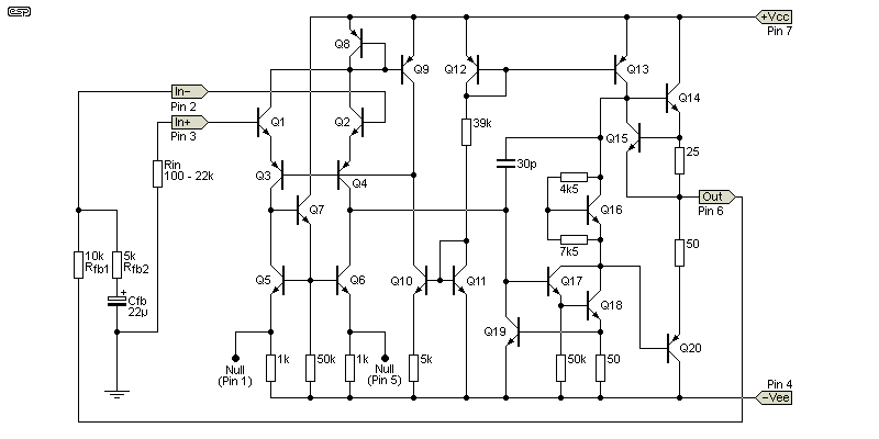
Figure 2.1 - Typical Voltage Feedback Opamp (µA741)
Rather than 'invent' a schematic, I've elected to use the µA741 as an example. It's not a fast device by any stretch of the imagination, with a quoted slew-rate of only 0.5V/ µs, and a unity gain bandwidth of just 1MHz. I used it here simply because it's one of the few opamps with a (more-or-less) complete schematic, and I had already converted it to my 'normal' ESP drawing style. It's also instructive in its own right, and worthy of analysis (by you, not me  ).
).
Unlike the CFB opamp circuits shown, you don't need to build a discrete VFB opamp, and the sensible approach is to use something that you have on hand if you wish to experiment. The µA741 might be a bit too pedestrian for any useful high-frequency response, but it's also a good starting point.
The next circuit is for a CFB opamp, using common, readily available transistors. I didn't use a commercially available circuit, but one that's widely referenced on the Net. The input ('In+') stage is a buffer, using complementary emitter followers. Feedback is applied to the emitters of Q3 and Q4, which is a low-impedance point in the circuit. Although feedback is applied in the same way (a feedback resistor from 'Out' to 'In-' (Rfb1), with a second resistor from 'In-' to ground - Rfb2), the resistors used will be much lower values than you'd use for a VFB opamp delivering the same gain.

Figure 3.1 - Typical Current Feedback Opamp
When feedback is applied (1k, 500Ω 220µF and Rin as 10k to ground), DC offset is 32mV, and doesn't change appreciably regardless of the resistance from 'In+' to ground. With values from 100Ω to 22k, it remains between 31 and 32mV. It's easy to see why it's claimed that CFB opamps are not recommended where DC offset performance is important. Note that the circuit is fully balanced (inasmuch as NPN and PNP transistors can be considered 'equal but opposite'), but DC offset is still terrible.
The LF -3dB frequency is still 1.45Hz. The HF -3dB frequency is over 10MHz, and a healthy 8V peak signal (5.7V RMS) is available at 5MHz (distortion is under 2%). If Rfb1 is reduced to 500Ω and Rfb2 is 250Ω, the -3dB frequency is increased to 28MHz! Note that that is the only change. The bandwidth is inversely proportional to the feedback resistance, so as Rfb1 is reduced, the bandwidth is increased. Even if the gain is increased from three to six (Rfb2 at 100Ω), the bandwidth still extends to 23.5MHz.
This is where the CFB circuit excels. Even with no compensation capacitor (which is essential in a VFB circuit), the Figure 3 opamp remains stable at any gain you desire - at least in the simulator. Real-life is different of course, but having recently played around with a small CFB power amplifier, I know that extraordinary high-frequency performance is quite easy to achieve. Mostly it is necessary to include a compensation capacitor, if only to prevent the circuit from amplifying RF or oscillating due to stray capacitance from output to input (only a few pF is usually needed).
While balanced CFB circuits have slightly better DC performance than those with a single transistor input, it's still mediocre. The Figure 3.1 circuit is simplified from the version you'll see elsewhere (including two of the references), but it's still somewhat 'over the top' for anyone who wants to play with the idea, so a simpler version is shown below. The Figure 3.2 circuit has actually been on the ESP website for a long time, as the Project 37 DoZ preamplifier, but without the output buffer stage.
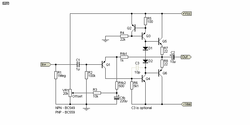
Figure 3.2 - P37 (DoZ - Modified) Current Feedback Opamp
As you'd expect, the performance can't match that of the Figure 3.1 circuit. With only a single input transistor, the DC offset is large, and VR1 is essential to reduce it to something 'sensible' (±50mV or so). For the convenience of comparisons, it's set for the same gain as Figures 2.1 & 3.1, at ×3. The simulator claims -3dB at 10MHz (without C3, which is optional), and based on tests I've run that's probably about right, but not with full output level. Getting 5.5V RMS at 100kHz is easy, and that's respectable for such a simple amplifier. Note that I added an output buffer stage so the circuit won't struggle with low-impedance feedback networks. This was not necessary with the original P37.
The frequency response of the two circuits is interesting. The VFB opamp is the µA741 shown in Figure 2.1, and the only thing that was changed was the feedback resistors. The ratio was 2:1 (Rfb1:Rfb2) in each case, and the response was plotted from 10kHz to 100MHz. While there is some variation with the VFB opamp, it's only slight. In fact it's so small that the traces are perfectly overlaid and they can't be separated, but all four are in the graph. Note that in both cases (VFB and CFB), the response is theoretical, and would typically only apply at low signal levels.
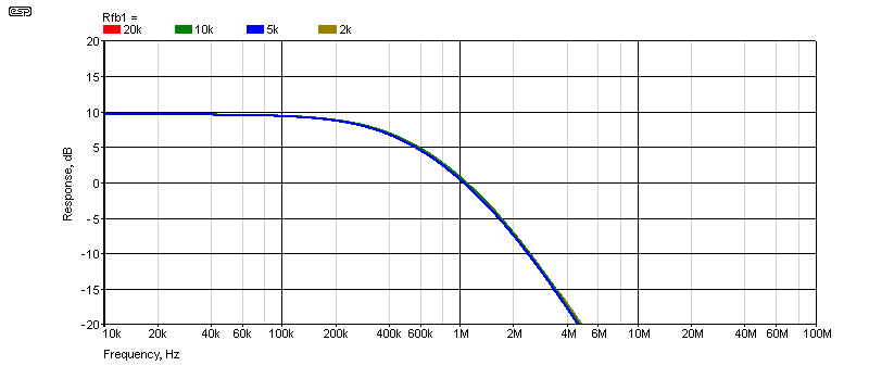
Figure 4.1 - Fig 2.1 VFB Opamp Response
In contrast, when the feedback resistors are changed with a CFB opamp (Figure 3.2 circuit, without C3), the response change is very apparent. Nothing else was changed - only the feedback resistors, and always with a ratio of 2:1 (Rfb1 and Rfb2 respectively). As the feedback resistance is reduced, the bandwidth is increased. This is completely normal with all CFB opamps, and it's usually included in the datasheet in graphical form. This makes it easy to control the frequency response simply by selecting the value of Rfb1, with Rfb2 setting the gain.
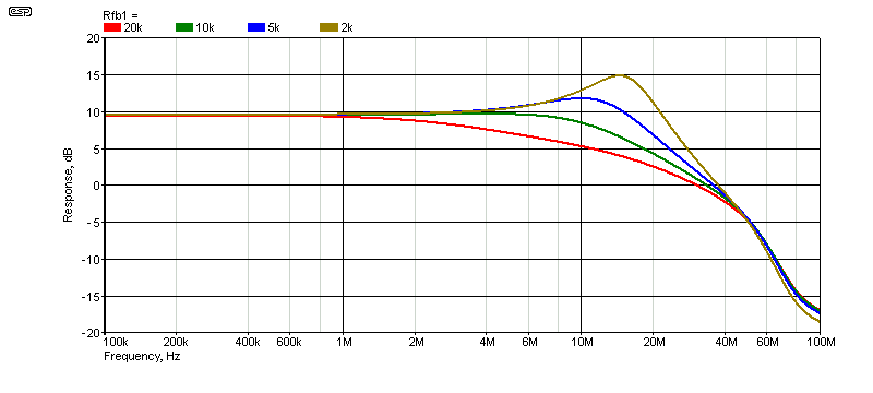
Figure 4.2 - Fig. 3.2 CFB Opamp Response
I also measured the rise and fall times for both circuits. The VFB opamp (µA741) managed 0.54V/µs rise and fall, while the CFB opamp was much faster, with 52V/µs rise time and a very fast 329V/µs fall time. These were both taken with Rfb1 at 2k, so it's possibly pessimistic for the CFB opamp, but as the frequency response shows, it makes no appreciable difference for the VFB version. With all VFB opamps, the slew rate is determined by the dominant pole capacitor, and feedback doesn't change that. Without C3 (10pF) the CFB opamp shows ringing when a 2k resistor is used for Rfb1. Adding C3 reduces the slew-rate to 12V/µs rise and 55V/µs fall.

Figure 4.3 - Fig. 3.2 CFB Opamp Transient Response
The rise and fall times for the Figure 3.2 CFB opamp are shown above. This shows the output response vs. the input, and the ringing is clearly evident. The graph was taken without C3 (10pF) to demonstrate the 'worst-case' behaviour. The ringing can be predicted from the frequency response (brown trace, 2k for Rfb1) which shows a 5dB peak at around 15MHz. Note that the rise and fall time of the input signal is 5ns, which is easy to get in a simulator, but a little harder in real life.
The slew rates are different due to the VAS transistor (Q4). It can turn on very quickly so fall time is short, but it takes longer to turn off again, due to base storage within the transistor itself. This is made worse when the transistor is driven into saturation (minimum collector voltage). A transistor specifically designed for high-frequency operation (such as an RF transistor) will improve this. The wider bandwidth will make the response peak greater, so compensation becomes a requirement rather than an option.
Another major difference is the open-loop gain. This is measured using only the DC feedback resistor (Rfb1), with an 'infinitely large' capacitance from the inverting input to ground. This is easy to do in a simulator, but is somewhat more difficult to do on the workbench (to put it mildly). Typically, the capacitance used will be over 1F (yes, 1 Farad or more).
I also simulated a TL072, which has a slew-rate of 13V/µs. Like the µA741, it showed an almost identical response when the feedback resistors were changed while retaining the same ratios. I varied Rfb1 from 2k to 100k, and Rfb2 from 1k to 50k. The upper -3dB frequency remained at 1.3MHz in the simulator, which agrees with the datasheet. At that frequency, there is almost zero feedback, because the IC runs out of gain (according to the datasheet, unity gain bandwidth is 3MHz). This is what we should expect, as the TL07x series was not designed for high frequency operation.
For the µA741 VFB circuit, open-loop gain reaches 107dB at low frequency, but is 3dB down at only 5Hz, and rolls off at 6dB/ octave. The gain is reduced to 21dB at 100kHz. In contrast, even the simple CFB circuit (Figure 3.2) has an open-loop gain of 80dB at low frequencies, 74dB at 7kHz, and has 57dB of gain at 100kHz. The Figure 3.1 CFB opamp has slightly higher low-frequency gain (87dB), and it rolls off later (-3dB at 14kHz). At 100kHz it still has 70dB of gain. This was simulated using a 2k feedback resistor (Rfb1).
You may well ask why open-loop gain is of any interest. It lets you determine how much feedback is applied at any given frequency. If an audio preamp (or power amp) is expected to have 30dB of gain, should the open loop gain at 20kHz be only (say) 34dB (rolling off at 6dB/ octave from 100Hz to 20kHz), then there's only 6dB of feedback available, where there may be 80dB at 100Hz (for example). The ability of the feedback to reduce distortion is severely compromised by so little reserve gain. As a result, distortion is increased ... as you would expect.
Many people complain that feedback increases the amplitude of high-order harmonics, but fail to understand that this isn't usually the case at all¹. Yes, upper harmonics may appear to rise alarmingly, but that's because there isn't enough gain at those frequencies for the feedback to be effective. It's usually not so much that the harmonics are increased, they aren't suppressed if there's not enough feedback. For feedback to be effective, there needs to be a lot of it, and the circuitry needs to have enough open-loop bandwidth to ensure that the feedback remains effective over the widest frequency range possible. This is harder with voltage feedback because of the requirement for a dominant-pole capacitor. However, with any competent opamp currently available, it's rarely a problem unless you expect a gain of (say) 100 (40dB) from a single stage.
¹ There are some instances where feedback can increase the level of harmonics, and this is covered in the article Distortion & Feedback. In most cases, this is only possible using circuits that are designed to show the effect, which is not helpful when considering 'real-world' circuitry. With most traditional designs, the increase in harmonic levels is due only to reduced feedback at high frequencies.
The poor DC performance of a CFB amplifier (whether small-signal or a power amplifier) can be improved by using a DC servo. This will invariably be a VFB opamp, selected for its low-frequency and DC performance. If properly configured it will have no effect on the audio. DC servo circuits are covered in detail in the article DC Servos - Tips, Traps & Applications. Figure 5 shows a modified version of the Figure 3.2 circuit, with the trimpot removed and replaced by the servo circuit (U1, R9, R10, C2 and C3). No output capacitor is used.
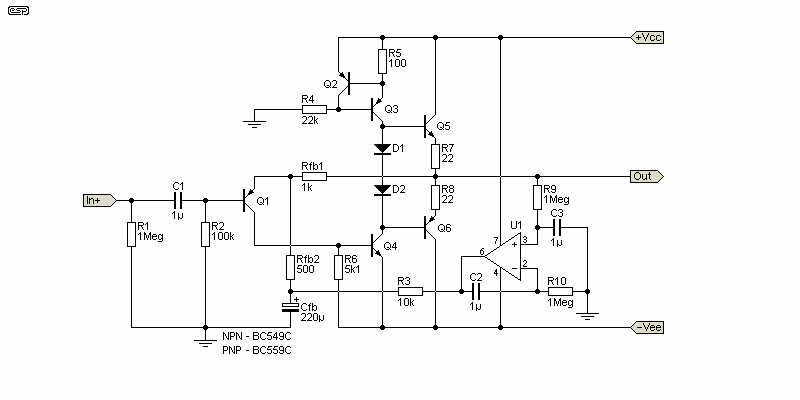
Figure 5 - CFB Opamp With DC Servo
By adding a DC servo, the output DC offset is reduced to the worst-case offset voltage of the opamp, but also determined by input offset current. For most 'ordinary' opamps the offset should be less than ±2mV, and if you need better than that you can use an 'exotic' opamp. Ideally, the opamp will have JFET inputs so the servo capacitance (C2) is kept to a reasonable value. With the servo, the output DC will be minimised even if the temperature of the circuit changes (especially Q1), something that isn't possible using the trimpot. Servos aren't without their own problems of course, but in this circuit there's nothing that will create any issues.
The servo does have some influence of the very low frequency performance, but since CFB circuits are generally used to get good high frequency performance, this should not cause any degradation. I suggest that the reader also reads the 'DC Servos' article, as that has full details of how it works. The use of a servo can be applied to any CFB amplifier if good DC performance is necessary. The simulator claims that the DC offset will be in the order of 130µV, which is about what I'd normally expect.
All servo systems have a settling time, determined by the filter time constant. With 1MΩ and 1µF as shown, the time constant is 1 second, but it will typically take at least twice that before the output voltage is close to zero. To avoid noise (typically a 'thump') when power is applied, a muting circuit is necessary if the noise will cause problems.
If you're used to looking at the specifications for VFB opamps, you could be forgiven for thinking that the idea of an opamp working to up to 100s of MHz can't be right. Not too many years ago you'd be correct, as CFB opamps only became readily available in the 1990s. They remain a niche product, and most people will never have used one or experimented with them. As I mentioned above, you may have built one without realising it, based on a couple of ESP projects. However, these were never intended to be used for radio frequencies and the subtleties would have escaped notice.

Figure 6 - THS6012 Frequency Response Vs. Feedback Resistance
The above graph is adapted from one in the datasheet for the THS6012 CFB differential line driver, specifically designed for ADSL (which is now a distant memory as cable or fibre-optic broadband has become available). Back in 2001, TI sent me a selection of CFB opamps to evaluate as headphone drivers. The THS6012 excelled in this role, but was unfortunately only available in an SMD package, and was very difficult to mount on a PCB as it had the heatsink tab on the underside of the package.
I ran many tests on it, and it could not really be faulted, although the low input impedance and heatsink requirements made it impractical to use it in a project. That's a shame, because its performance was exemplary, but the package made it impractical.
I have deliberately left out the complex formulae that can be used to analyse these circuits mathematically. Most readers won't be interested, and for the few who do want to perform detailed analysis, the references have everything you need. Like many references, expect to find errors - it's very hard to ensure that all details are exactly right, and you'll quickly discover that the Figure 3.1 circuit has been used as the 'gold standard' for CFB opamps. There are more complex versions as well, but it's already a fairly daunting circuit (I'm certainly not about to build one).
For the most part, CFB opamps will remain a curiosity for most hobbyists, unless working with RF. Radio (and video) frequencies are easily handled by many readily available CFB opamps. Frequency response to over 300MHz is not uncommon, with slew rates of 1kV/µs or more. These are specialised, but even 'ordinary' CFB opamps are capable of 100MHz bandwidth (at low output levels). Power amplifiers are a different matter. A 'practice' amplifier (for learning how power amps work) is published as Project 217, and it uses current feedback. It can't achieve MHz bandwidth, but that's a limitation that was deliberately imposed to ensure stability. There are a few other power amps that use current feedback, including Project 36 (DoZ) and its preamp, Project 37.
As noted in the introduction, one must be careful to differentiate between the two types of current feedback. Project 27 (guitar amplifier) uses current feedback too, but to monitor the output current and adjust the gain accordingly. The amp itself uses a VFB circuit, rearranged to provide current feedback. While this may create a little confusion at first, the two types are very different. To complicate the situation even more, it's quite simple to have a 'true' CFB amplifier reconfigured (via the feedback network) to provide a defined output current, which I suppose would make it a 'current feedback - current feedback' amplifier!
Main IndexArticles Index