

|
| Elliott Sound Products | The 555 Timer |
 Main Index
 Articles Index
The 555 timer has been with us since 1972 - that's a long time for any IC, and the fact that it's still used in thousands of designs is testament to its usefulness in a wide variety of equipment, both professional and hobbyist. It can function as an oscillator, a timer, and even as an inverting or non-inverting buffer. The IC can provide up to 200mA output current (source or sink) and operates from a supply voltage from 4.5V up to 18V. The CMOS version (7555) has lower output current and also draws less supply current, and can run from 2V up to 15V.
There are many different manufacturers and many different part number prefixes and suffixes, and they are available in a dual version (556). Some makers have quad versions as well. The 555 and its derivatives come in DIP (dual in-line package) and SMD (surface mount device) packages. I don't intend to even attempt to cover all the variations because there are too many, but the following material is all based on the standard 8 pin package, single timer. All pin numbers refer to the 8-pin version, and will need to be changed if you use the dual or quad types, or choose one of the SMD versions that has a different pinout. Note that the quad version has only the bare minimum of pins, reset and control voltage are shared by all four timers, and it has no separate threshold and discharge pins (they are tied together internally, and called 'timing').
The 555 uses two comparators, a set-reset flip-flop (which includes a 'master' reset), an output buffer and a capacitor discharge transistor. A great many of the functions are pre-programmed, but a control input allows the comparator threshold voltages to be changed, and many different circuit implementations are possible. A block diagram is useful, and Figure 1A shows the essential parts of the IC's innards.
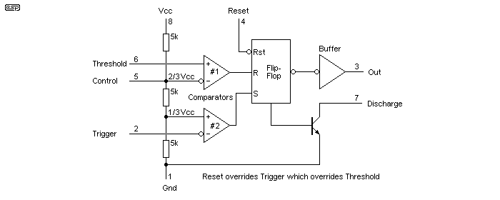
Figure 1A - Internal Diagram Of 555 Timer
Figure 1B shows a complete circuit diagram for a 555 timer, based on the schematic shown in the ST Microelectronics datasheet. Schematics from other manufacturers may differ slightly, but the operation is identical. There's really not much point in going through the circuit in detail, but one thing that needs to be pointed out is the voltage divider that creates the reference voltages used internally. The three 5k resistors are shown in blue so you can find them easily, and the main sections are shown within dotted lines (and labelled) so each section can be identified.
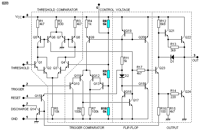
Figure 1B - Schematic Of 555 Timer
Unless you are very experienced in electronics and can follow a detailed circuit such as that shown, it probably won't mean a great deal to you. It is interesting though, and if you were to build the circuit using transistors and resistors it should work very much like the IC version. Note that there are often extra transistors in ICs because they are cheap to add (essentially free), some are parasitic, and the performance of NPN and PNP transistors is never equal. In most cases IC production is optimised for NPN, and PNP devices will nearly always have comparatively poor performance.
The standard single timer package has 8 pins, and they are as follows. The abbreviations for various functions that are used throughout this article are included in brackets.
Pin 1 Common/ 'ground' (Gnd) This pin connects the 555 timer's circuitry to the negative supply rail (0 V). All voltages are measured with respect to this pin.
Pin 2 Trigger (Trig) When a negative pulse is applied (a voltage less than 1/3 of Vcc), this triggers the internal flip-flop via comparator #2. Pin 3 (output) switches from 'low' (close to zero volts) to 'high' (close to Vcc). The output remains in the high state while the trigger terminal is maintained at low voltage, and the trigger input overrides the threshold input.
Pin 3 Output (Out) The output terminal can be connected to the load in two ways, either between output and ground or output and the supply rail (Vcc). When the output is low, the load current (sink current) flows from Vcc, through the load into the output terminal. To source current the load connects between the output and common (0V). If the load is connected between the output and ground, when the output is high current flows from the output, through the load and thence to ground.
Pin 4 Reset (Rst) The reset pin is used to reset the flip-flop which determines the output state. When a negative pulse is applied to this pin the output goes low. This pin is active low, and overrides all other inputs. It must be connected to Vcc when it is not in use. Activating reset turns on the discharge transistor.
Pin 5 Control voltage (Ctrl) This pin is used to control the trigger and threshold levels. The timing of the IC can be modified by applying a voltage to this pin, either from an active circuit (such as an opamp) or by connecting it to the wiper of a pot connected between Vcc and ground. If this pin is not used it should be connected to ground with a 10nF capacitor to prevent noise interference.
Pin 6 Threshold (Thr) This is the non-inverting input for comparator #1, and it monitors the voltage across the external capacitor. When the threshold voltage is greater than 2/3 Vcc, the output of the comparator #1 goes high which resets the flip-flop and turns the output off (zero volts).
Pin 7 Discharge (Dis) This pin is connected internally to the collector of the discharge transistor, and the timing capacitor is often connected between this pin and ground. When the output pin goes low, the transistor turns on and discharges the capacitor.
Pin 8 Vcc The supply pin, which is connected to the power supply. The voltage can range from +4.5v to +18v with respect to ground (pin 1). Most CMOS versions of the 555 (e.g. 7555/ TLC555) can operate down to 2 or 3V. A bypass capacitor must always be used, not less than 100nF and preferably more. I suggest 10µF for most applications.
As mentioned above, the 555 can be used as an oscillator or timer, as well as to perform some less conventional duties. The basic forms of multivibrator are the astable (no stable states), monostable (one stable state) or bistable (two stable states). Unfortunately, operation as a bistable is not very useful with a 555 because of the way it's organised internally. However, it can be done if you accept some limitations. A 555 circuit that functions as a bistable is described in Project 166, where the 555 is used as a push-on, push-off switch for powered equipment.
The timing is fairly stable with temperature and supply voltage variations. The 'commercial grade' NE555 is rated for a typical stability of 50ppm (parts per million) per degree C as a monostable, and 150ppm / °C as an astable. It's worse as an oscillator (astable) than a timer (monostable) because the oscillator relies on two comparators but the timer only relies on one. Drift with supply voltage is about 0.3% / V.
Most of the circuits shown below include an LED with its limiting resistor. This is entirely optional, but it helps you to see what the IC is doing when you have a slow astable or timer. The circuits also show a 47µF bypass capacitor, and this should be as close to the IC as possible. If the cap is not included, you may get some strange effects, including a parasitic oscillation of the output stage as it changes state.
When the output is high, it will typically be somewhere between 1.2V and 1.7V lower than the supply voltage, depending on the current drawn from the output pin. The output stage of a 555 cannot pull the level to Vcc because it uses an NPN Darlington arrangement that will always lose some voltage, and the voltage will fall with increasing current. It's not usually a limitation, but you must be aware of it. If it's a problem you can add a pull-up resistor between 'Out' and 'Vcc' (1k or thereabouts), but it will only be useful for light loads (less than 1mA).
It should be made clear that the 555 is not a precision device, and this wasn't the intention from the outset. It has many foibles, but in reality they rarely cause problems if the device is used as intended. Sometimes it will be necessary to ensure that it gets a good reset on power-up so it's in a known state, but for most applications that's not necessary. If you really do need precision, use something else (which will be considerably more complex and expensive). It's been said that Bob Pease (from National Semiconductor, now TI) that he didn't like the 555 and never used them (see the Electronic Design website), but that's no reason to avoid them. Trying to use a 555 in a critical application where accuracy is paramount would be silly, but so is using a microcontroller with a crystal oscillator to perform basic timing functions.
As many readers will have noticed, I will generally use an opamp, a comparator or even some discrete circuitry in preference to a 555 timer. This isn't because I don't like the 555 IC, but simply because so few applications I normally work with need the flexibility it offers. It's certainly not a precision device, but it is handy, and countless circuits (many of them hobbyist designs) have used it - often because the designer doesn't know how to get a time delay by any other means.
It's a fairly simple process to build a discrete '555-like' circuit, and it only needs a handful of parts. You need at about 8 transistors, a few resistors and a couple of diodes to build a circuit that will perform reasonably well. In a simple implementation you won't have the reset pin, as that would add quite a few extra parts. I did simulate a simple version that (mostly) works, however, I really don't think there's much point because the IC is cheap, and takes up far less space on a PCB or breadboard.
Note: One thing to be aware of is the well-documented supply current spike created as the output changes state (particularly from low to high). While I have seen it claimed that this current spike can exceed 400mA, no one I know has experienced this. It's easily simulated, and my simulation showed a peak current of around 100mA, lasting for about 100ns (0.1µs). A bypass capacitor is always needed to handle this, and the minimum is 10µF. In the drawings below I used 47µF, which will usually mitigate supply voltage disturbances.
The oscillator (or to be correct - astable multivibrator) is a very common application, and therefore will be covered first. Note that all circuits below are assumed to be using a 12V DC supply unless otherwise noted.
The term 'astable' means, literally, 'not stable' - the very definition of an oscillator. The output switches from high to low and back again as long as power is available and the reset pin is maintained high. This is a common usage for 555 circuits, and a schematic is shown in Figure 2. The pulse repetition rate is determined by the values of R1, R2 and C1.
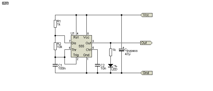
Figure 2 - Standard Astable Oscillator
The waveforms at the output and the voltage across C1 are shown below. The output goes high when the capacitor voltage falls to 4V (1/3 Vcc of 12V), and goes low again when the capacitor voltage reaches 8V (2/3 Vcc). The oscillator has no stable state - when the output is high it's waiting for the cap to charge so it can go low again, and when low it's waiting for the cap to discharge so it can go high. This continues as long as the reset pin is held high. Pulling the reset pin low (less than 0.7V) stops oscillation.

Figure 2A - Standard Astable Oscillator Waveforms
C1 is charged via R1 and R2 in series, and is discharged via R1. By default, this means that the output is a pulse waveform, rather than a true squarewave. The output will be positive, with negative-going pulses. If R2 is made large compared to R1 you can approach a squarewave output. For example if R1 is 1k and R2 is 10k ohms, the output will be close to a 1:1 mark-space ratio (it's actually 1.1:1). To determine the frequency, use the following formula ...
f = 1.44 / ((R1 + ( 2 × R2 )) × C1 )
For the values shown in Figure 2, the frequency calculates to 686Hz, and the simulator claims 671Hz. This may seem like a large discrepancy, but it's well within the tolerance of standard components and the IC itself. High and low times can be determined as well ...
t high = 0.69 × ( R1 + R2 ) × C1
t low = 0.69 × R2 × C1
With the values given in Figure 2, t high is 759µs and t low is 690µs. The simulator (and real life) will be slightly different. The duty cycle/ mark-space ratio is 1.1:1, and is calculated by the ratio of t high / t low. The high time is 1.1 times the low time, which makes perfect sense based on the resistor values. As R1 is made smaller the mark-space ratio gets closer to 1:1 but you must ensure that it's not so low that the discharge transistor can't handle the current. The maximum discharge pin current should not exceed 10mA, and preferably less.
You may well wonder where the values of 1.44 and 0.69 come from. These are constants (or 'fudge factors' if you prefer) that have been determined mathematically and empirically for the 555 timer. They're not perfect, but are close enough for most calculations. If you need a 555 circuit to oscillate at a precise frequency you'll need to include a trimpot so the circuit can be adjusted. It still won't be exact, and it will drift - remember that this is not a precision device and must not be used where accuracy is critical.
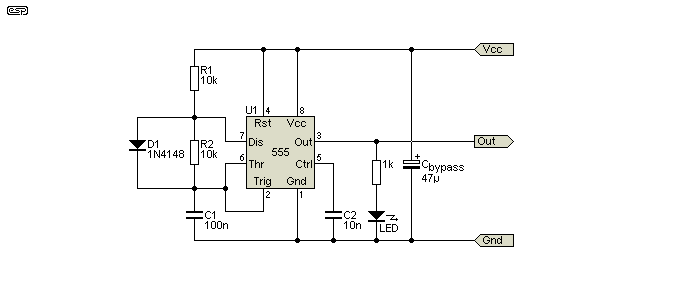
Figure 3 - Extended Duty-Cycle Astable Oscillator
By adding a diode, the operation is changed and simplified. C1 now charges via R1 alone, and discharges via R2 alone. This removes the interdependency of the two resistors, and allows the circuit to produce any duty-cycle you wish - provided it's within the 555's operating parameters of course. Pulses can now be narrow positive-going or negative-going, and an exact 1:1 mark-space ratio is possible. Frequency is determined by ...
f = 1.44 / ((R1 + R2 )) × C1 )
If R1 is greater than R2, the output will be positive with negative going pulses. Conversely, if R1 is less than R2 the output will at zero volts with positive pulses. The length of the pulse (positive or negative going) is therefore determined by the two resistors, and each is independent of the other. There is a small error introduced by the diode's voltage drop, but in most cases it will not cause a problem. The (ideal) high and low times are calculated by ...
t high = 0.69 × R1 × C1
t low = 0.69 × R2 × C1
Finally, there a circuit that's commonly referred to as the 'minimum component count' astable. Apart from the basic support parts that are always needed (the bypass capacitor and the cap from 'Control' to ground), it requires just one resistor and one capacitor.

Figure 4 - Minimum Component Astable Oscillator
The mark-space ratio of this circuit is nominally 1:1 (a squarewave) but this can be affected by the load. If the load connects between the output and ground, the high time will be a little longer than the low time because the load will prevent the output from reaching the supply voltage. If the load connects between the supply and output pin, the low time will be longer because the output will not reach zero volts. Frequency is calculated from ...
f = 0.72 / ( R1 × C1 )
With the values shown it will be 720Hz. You can see that the discharge pin (Pin 7) is not used. The capacitor is charged and discharged via R1, so when the output is high the cap charges, and when low it discharges. The discharge pin can be used as an open collector auxiliary output, but do not connect it to a supply voltage greater than Vcc, and don't try to use it for high current loads (around 10mA maximum).
All of the circuits shown use the internal voltage divider (3 × 5k resistors) to set the comparator thresholds. Whenever the voltage reaches the threshold voltage (2/3 of Vcc) the flip-flop resets and the output is low (close to zero volts). When the trigger (Pin 2) voltage falls below 1/3 of Vcc the circuit is triggered and the output is high (close to Vcc).
If reset (pin 4) is pulled low at any time, the output goes low and stays there until the reset pin goes high again. The threshold voltage of the reset input is typically 0.7V, so this pin has to be connected directly to ground with a transistor or switch. An external resistor is required between Vcc and reset if you need to use the reset facility, as there is no pull-up resistor in the IC. In general, you can use up to 10k.
A monostable (also known as a 'one-shot' circuit) has one stable state. When triggered it will go to its 'unstable' state, and the time it spends there depends on the timing components. A monostable is used to produce a pulse with a predetermined time when it's triggered. The most common use of a monostable is as a timer. When the trigger is activated, the output will go high for the preset time then fall back to zero. While we tend to think of timers being long duration (several seconds to a few minutes), monostables are also used with very short times - 1ms or less for example. This is a common application when the circuit needs pulses with a defined and predictable width, and having fast rise and fall times.
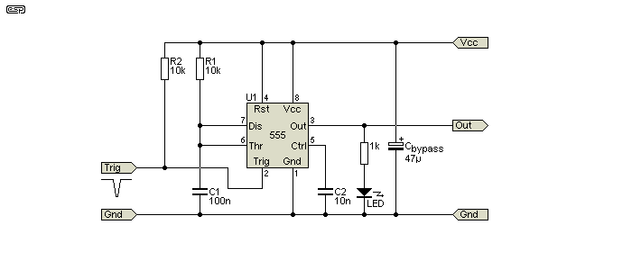
Figure 5 - Monostable Multivibrator
The trigger signal must be shorter than the time set by R1 and C1. The circuit is triggered by a momentary low voltage (less than 1/3 Vcc), and the output will immediately go high and remain there until C1 has charged via R1. The time delay is calculated by ...
t = 1.1 × R1 × C1
With the values shown, the output will be high for 1.1ms. If C1 were 100µF, the time would be 1.1 seconds. As noted, the trigger pulse must be shorter than the delay time. If the trigger were to be 5ms long in the circuit shown in Figure 5, the output would remain high for 5ms and the timer has no effect. Apart from timers, monostables are commonly used for obtaining a pulse with a predetermined width from an input signal that is variable or noisy.
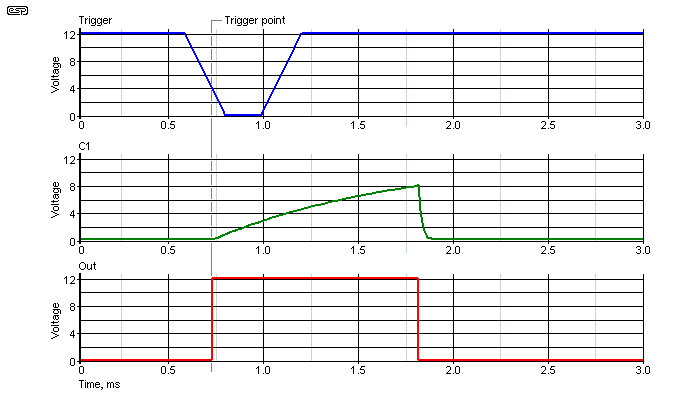
Figure 5A - Monostable Multivibrator Waveforms
It's helpful to see the waveforms for the monostable circuit. It's especially useful to see the relationships between the signal on the trigger pin and capacitor voltage in relationship to the output. These are shown above, and can be verified on an oscilloscope. You need a dual trace scope to be able to see two traces at the same time. As you can see, the timing starts when the trigger voltage falls to 4V (a 12V supply was used, and 4V is 1/3 Vcc). When the cap charges to 8V (2/3 Vcc) timing stops and the output falls to zero. Note that the cap charges from zero volts in this configuration, because C1 is completely discharged when the timing cycle ends.
The most common use of the monostable 555 circuit is as a timer. The trigger might be a push-button, and when pressed the output goes high for the preset time then drops low again. There are countless applications for simple timers, and I won't bore the reader with a long list of examples.
The timing components are fairly critical, in that they must not be so large or so small that they cause problems with the circuit. Electrolytic capacitors are especially troublesome because their value may change with time, temperature and applied voltage. Wherever possible, use polyester caps for C1, but not if it means that the resistor (R1) has to be more than a few Megohms. The threshold pin may only have a leakage of 0.1µA or so, but if R1 is too high even this tiny current becomes a problem. The capacitor is always the limiting factor for long time delays, because you will almost certainly have to use an electrolytic. If this is the case, use one that is classified as 'low-leakage' if possible. Tantalum caps are often suggested, but I never recommend them because they can be unreliable.
Sometimes, you can't be sure that the input pulse will be shorter than the time interval set by R1 and C1. If this is the case, you need a simple differentiator that will force the input pulse to be short enough to ensure reliable operation. Differentiators require that the rise and/ or fall times are much faster than the time constant of the differentiator itself. For example, a 10nF cap with a 1k resistor has a time constant of 10µs, so the rise/ fall time of the input pulse should ideally not be more than 2µs or it may not work properly. The ratio of 5:1 is a guide only, so you need to check what is available from your other circuitry. Ideally, use a ratio of 10:1 or more if possible (i.e. differentiator time constant of 10 times the risetime of the input signal).
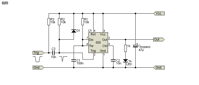
Figure 6 - Monostable Multivibrator With Differentiator
R3, C3 and D1 form the differentiator circuit. When a pulse is received, the cap can only pass the falling edge, which must be as fast as possible. This is passed on to the 555, and it no longer matters how long the input trigger pulse remains negative, because the short time constant of C3 and R2 (100µs) only allows the falling edge to pass through. D1 is necessary to ensure that Pin 2 cannot be made more positive than Vcc plus one diode drop (0.65V) when the trigger pulse returns to the positive supply.
If the input trigger pulse fall time is too slow, the differentiator may not pass enough voltage to trigger the 555. If this is the case, the signal will have to be 'pre-conditioned' by external circuitry to ensure that the voltage falls from Vcc to ground in less than 20µs (for the values shown). If this isn't done, the circuit may be erratic or it might not work at all. If your trigger pulse is positive-going, you'll have to invert it so that it becomes negative-going. The 555 is triggered on the falling edge of the trigger signal, which causes the output to go high (Vcc).
Hint: If you happen to need a timer that runs for a long time (hours to weeks), use a variable 555 oscillator circuit that then drives a CMOS counter such as the 4020 or similar. The output of the 555 oscillator might be (say) a 1 minute/ cycle waveform, and that can act as the clock signal for the counter. The 4020 is a 14 bit binary counter, so with a simple circuit you can easily get a delay (using a 1 minute clock) of 8,192 minutes - over 136 hours or a bit over 5½ days. Still not long enough? Use two or more 4020 counters. Two will allow a timer that runs for about 127 years! Note that you will have to provide additional circuitry to make any of this work, and it may be difficult to be certain that a 127 year timer works as expected. 
Here's an example (but it's not a monostable), and depending on the output selected from the 4020 counter you can get a delay of up to 20 minutes. If C1 is made larger the delay can be much greater. With the resistor values given for the timing circuit, increasing C1 to 100µF will extend the maximum time to 3.38 hours (3h 23s), using Q14 of U2 as the output. If C1 is a low leakage electro, the values for R1 and R2 can be increased, so it will run for even longer. The drawing also shows how many input pulses are required before the respective outputs go high (Vcc / Vdd). The counter advances on the negative-going pulse. To use higher value timing resistors, consider using a CMOS timer (e.g. 7555).
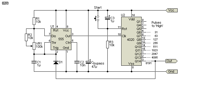
Figure 7 - Long Duration Timer
As shown, the minimum period for the 555 is 20.83ms (48Hz) with VR1 at minimum resistance, and at maximum resistance it's 145.7ms (6.86Hz). When power is applied the timer will run for the designed time period until the output goes high. Pressing the 'Start' button will set the output low and the time period starts again. All outputs from the counter are set low at power-on by the reset cap (C3) and/ or when the 'Start' button is pressed. The 555 runs as an astable, and continues pulsing until the selected output from U2 goes high. D1 then forces the voltage across C1 to 0.7V below Vcc and stops oscillation. Therefore, when the 'Start' button is pressed the output goes low, and returns high after the timeout period.
Additional circuitry is needed if you don't want the timer to operate after power-on, or if you want the 'Start' button to make the output high, falling to zero after the timeout. I leave these as an exercise for the reader. The above is simply an example - it's not intended to be a circuit for any particular application.
There are many uses for 555 timers apart from the basic building blocks shown above. This is an article and not a complete book, so only a few of the possibilities will be covered. They have been selected based on things I find interesting or useful, and if you have a favourite that isn't included then that's just tough I'm afraid. 
Don't expect to find sirens, general purpose noisemakers or pseudo random 'games' in amongst the things here. If you want to build any of the popular 555 toys, there are plenty to be found on the Net.
This is a simple PWM (pulse width modulation) dimmer or motor speed controller. It's based on the 'minimum component' astable shown earlier, but uses a pot and a pair of diodes to vary the mark-space ratio. When the pot is at the 'Max' setting, the output is predominantly high, with only narrow pulses to zero. When at the 'Min' setting, the output is mostly at zero, with narrow positive pulses.
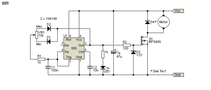
Figure 8 - PWM Dimmer/ Motor Speed Controller
The way it works is no different from the basic astable, except that the amount of resistance for capacitor charge and discharge is variable by means of the pot. The diodes (1N4148 or similar) 'steer' the output current so that the pot has the ability to have a different resistance depending on the signal polarity. For example, when the pot is at 'Max', it takes much longer to charge C1 than to discharge it, so the output must spend most of its time at Vcc. The converse applies when the pot is set to 'Min'. The maximum and minimum duty-cycle can be altered by changing R1. With 1k as shown, the maximum is 11:1 (or 1:11), but making R1 smaller or larger can change this to any ratio desired (within reason). I suggest that 100 ohms is a practical minimum.
To be useful, the output of the 555 will normally drive a MOSFET as shown, or perhaps even an IGBT, depending on the load current. If it's used as a motor speed controller, you must include a diode in parallel with the motor or it will not work properly. The diode has to be a 'fast' or 'ultra-fast' version, and rated for the same current as the motor. The diode isn't needed if the circuit is used as a dimmer, but it's a good idea to use a UF4004 or similar fast diode anyway. The supply to the motor can be anything you like (DC only), but the 555 must have a 12-15V supply, separate from the main supply if necessary. See Project 126 for a project version of a dimmer/ speed controller. It doesn't use a 555, but uses the same PWM principles.
A 555 can be made to work as a PWM (Class-D) amplifier. It's not very good and output power is very limited, but you can get up to 100mW or so into an 8 ohm load. It's a purely educational exercise more than anything else, because fidelity is not great due to the limited performance of the 555. Maximum frequency is 500kHz or so, but the IC will almost certainly overheat if operated at maximum frequency and output current. I won't bother showing a practical circuit for a Class-D amp using a 555 because the performance is so poor. Suffice to say that if you inject a sinewave or music signal into the 'Ctrl' pin, you can modulate the pulse width. The same trick is used for many of the 555 based sirens that you can find elsewhere.
The control input is often overlooked, but it can be used any time you need to create a voltage-controlled oscillator. Apart from toy sirens and other 'frivolous' applications, this ability can be useful for many circuits. Just because the 555 is a rubbish Class-D amplifier doesn't mean that the general principles should be ignored. One application that's quite popular on the Net is using a 555 as the controller for a simple regulated high voltage supply. The drawing below is a modified version of one that is all over the Net (so much so that it's not possible to provide attribution because I have no idea who posted it first).
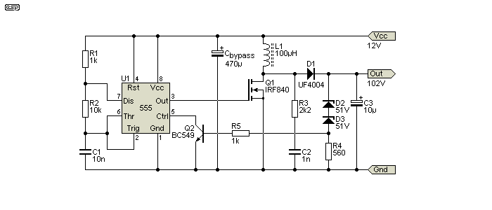
Figure 9 - DC-DC Converter
The circuit shown is largely conceptual. It will work, but is not optimised. The feedback applied to the control input is dependent on the zener voltages, and the emitter-base voltage of the transistor has little effect. There are ICs specifically designed for voltage sensing that use a voltage divider to set the output voltage, and this makes it easy to change the voltage to an exact value if necessary. The high-voltage zener string will provide surprisingly good voltage stability. The circuit is shown here simply to demonstrate the use of the control input to change the operation of the 555.
It will be able to deliver up to 50mA without much stress, but as with any step-up switchmode converter, the peak input current may be quite high. With the values shown and a 20mA output, the peak current will be around 2A. Naturally, if the output current is less than 20mA, input current is reduced proportionately. Start-up current will be much higher than the operating current. L1 (100µH) should have a resistance of no more than 1/2 ohm. An output of 100V at 20mA is 2W, so it's reasonable to expect the average input power to be somewhat greater. Losses will almost certainly be close to 1W in total, so the average input current will be around 250mA at 12V.
There are dedicated SMPS controllers that may be no more expensive than a 555 timer, but it's still a useful application and means you don't need to search for an obscure part. It's greatest advantage is that it can often be built using parts you already have in your junk-box, with the added benefit that it doesn't rely on SMD parts and can be built on Veroboard.
This is a useful circuit, and it can be used to drive simple transducers (small speakers, lamps, etc.). The maximum current the 555 can source or sink is about 200mA, so loads that draw more than that will cause the IC to overheat and fail. Because there are no support components needed at all, it can be very economical for PCB space. It's been claimed that using a discrete circuit with a pair of transistors is cheaper, but that's doubtful given the cost of a 555. The IC also takes up very little PCB real estate, something that's often far more expensive than a few cheap parts, especially is space is at a premium.
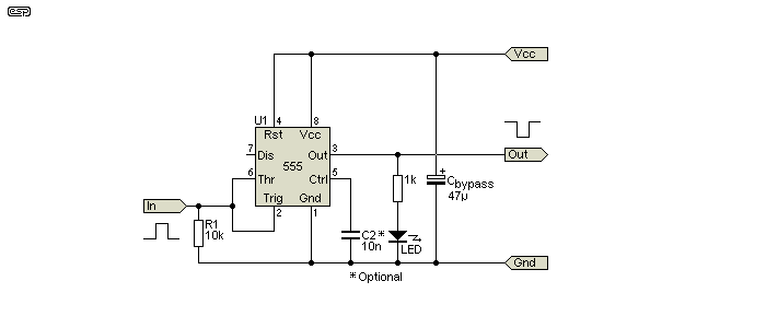
Figure 10 - Inverting Buffer
The input signal is subject to hysteresis. This means that the input voltage needs to exceed 2/3 Vcc before the output will switch low, and the input then needs to fall below 1/3 Vcc before the output will switch high. This provides very good noise immunity, and input impedance is very high. The circuit is an inverting Schmitt trigger.
This is a fairly uncommon application. By using the reset pin as an input, any voltage above ~0.7V is determined to be high, and the output will switch high. The input voltage must fall below 0.7V for the output to switch low again. There is no hysteresis, and the driving circuit needs to be able to sink the 555's reset pin current of about 1mA.
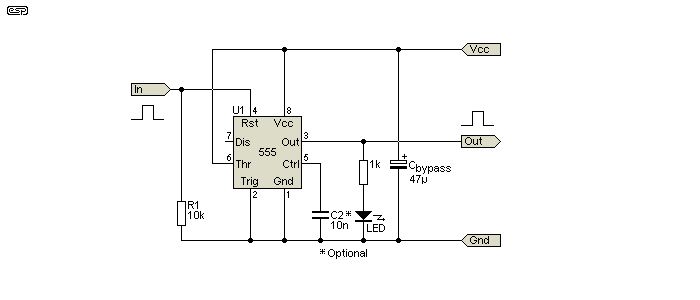
Figure 11 - Non-Inverting Buffer
You must be careful to ensure that the input to pin 4 can never exceed Vcc or become negative, or the IC will be damaged. If out-of-range excursions are possible, then the input voltage must be clamped with a diode, zener or both to keep the voltage within limits.
One quite common use for 555 timers is as a missing pulse detector. If you expect a continuous train of pulses from a circuit, should one go 'missing' for any reason that may indicate a problem. Being able to detect that a pulse is missing or delayed can be an important safety function, raising an alarm or disabling the circuit until the fault has been corrected.
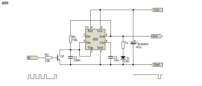
Figure 12 - Missing Pulse Detector
Input pulses are used to switch on Q1 and hence discharge C1. As long as the pulses keep arriving in an orderly manner the output of the 555 stays high. The time constant of R1 and C1 must be selected so that the timer can never expire as long as the input pulses keep arriving as they should. If the time is too short C1 will charge to 2/3 Vcc before the next input arrives. If it's too long, a single missing pulse won't be detected and it will require several pulses in a row to be missing (or the pulse train may stop altogether) before the timer will operate. You may also need to take precautions to ensure the timer will always operate, even if the incoming pulse train gets stuck at the high voltage level. This will involve adding a differentiator, similar to that shown in Figure 6.
One use for a missing pulse detector is to detect that a fan is not performing as it should. Some fans have an output that pulses when the fan is running, or the function can be added with two small magnets and a Hall effect detector (two magnets are needed so the fan's balance isn't affected). The missing pulse detector can raise an alert if a fan fails or is running too slow.
The circuit can also be used as a 'loss-of-AC' circuit, and will detect a single missing cycle or half cycle, depending on the detection mechanism used. This makes it capable of quickly detecting that AC has been removed, either by switching off or due to mains failure, and can be used to operate muting relays (for example). In most cases it's not necessary to be quite so fast, but there may be critical industrial processes where rapid detection of as little as one missing half-cycle may be crucial to prevent malfunction. This arrangement will also work well to ensure very fast changeover to a UPS (uninterruptible power supply) in cases where loss of AC may cause major problems.
Although a 555 can drive a relay directly, it has to be protected against the inductance of the relay coil. Back EMF should (in theory) be absorbed because the output has high-side and low-side transistors, but instead it can cause the timer to 'lock up' and cease to function until the power is cycled. This can happen when a single diode is used in parallel with the relay coil. Use the parallel diode, but also drive the relay coil via another diode which prevents any malfunction. The output must never be subjected to a negative voltage - even 0.6V can cause problems.

Figure 13 - Relay Driver
D2 performs the usual task of shorting out the relay's back EMF, and D1 completely isolates the relay circuit from the 555. Using this arrangement will prevent any possibility of malfunction due to the relay coil's back EMF, and the same arrangement should be used when driving any inductive load.
A 555 timer can make a handy mute circuit. There are countless different ways that muting can be achieved - see Muting Circuits For Audio for a range of different techniques. Of them all, a relay is still one of the best. Because contact resistance is very low, even low impedance circuits can be effectively shorted to ground with usually no audible breakthrough. All ESP circuits include a 100 ohm resistor at the output to prevent oscillation, and no common opamp can be damaged by placing a short at its output - with the resistor, the opamp is protected against a direct short anyway.
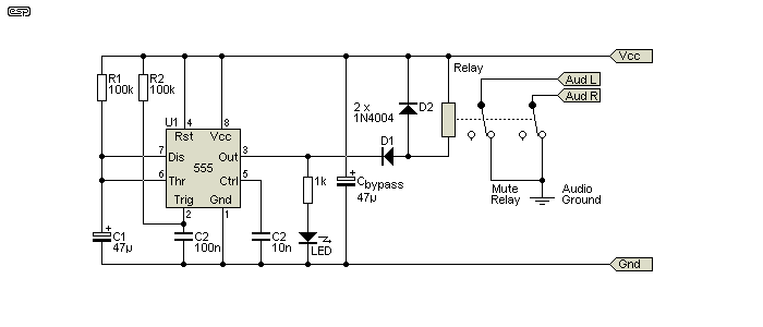
Figure 14 - Relay Mute Circuit
The circuit shown can be powered from the main preamp supply, or it can even be powered from a bridge rectifier across the 6.3V AC heater supply with valve (tube) equipment. If you do that, Cbypass should be around 220µF, and no other filter cap is needed. You will need to add a resistor in series with the coil to limit the voltage to 5V. The LED will be on for the duration of the mute period. The relay drive requires two diodes as discussed above. Most suitable relays will draw between 30 and 50mA, well within the capabilities of a 555.
The 555 gets a trigger signal by virtue of the cap from the trigger input (C2) and R2 is the pull-up resistor. C2 holds the trigger input low for just long enough to start the timing process, so the output is high, the relay is de-energised, and C1 starts charging via R1. When the voltage at the threshold input reaches 2/3 of the supply voltage, the output goes low, operating the relay and removing the short across the audio signal lines. If the supply voltage rises slowly the circuit may not work properly (or may not work at all), and you may need to increase the value of C2.
The relay remains energised for as long as the equipment remains powered. Ideally, the supply to the timer should be removed as quickly as possible when power is turned off to ensure that there are no 'silly' noises generated as the supplies collapse. Some opamps can create a thump, squeak or 'whistle' as their power supply drops below the minimum needed for normal operation. If you need a mute circuit, this is not one that I recommend. See the article Muting Circuits For Audio. Figure 12 is particularly recommended.
The 555 timer is very versatile, but is not really suited for very long time delays unless you are willing to pay serious money for a large, low-leakage timing capacitor. It's easier to use a 555 oscillator followed by a binary counter if you need long delays. Most applications will only call for delays of perhaps a few minutes (20-30 minutes is the suggested maximum), and this is easily achieved. The number of possible circuits using 555 timers is astonishing, and there are countless circuits, application notes (from IC manufacturers, hobbyists and others) and web pages devoted to this IC and its derivatives.
555 timers are used in many commercial products where a simple time delay is needed. I've seen them used in trailing edge and universal lamp dimmers, and (despite the comments in the introduction) have used them in several products I've developed over the years. The popularity of the 555 has not diminished despite its age, and it's safe to say that the number of applications has steadily increased, even with the use of digital techniques that supposedly render analogue 'obsolete'.
It's not at all unusual to find a 555 timer used in a switchmode power supply (SMPS), and simple low power supplies can be made with a 555 IC, a transformer and not much else. As with any IC there are limitations, and it's important to ensure that the IC is properly bypassed because they can draw up to 200mA as the output makes the transition between high and low or vice versa.
CMOS versions of the 555 (e.e. 7555) offer some useful advantages over the bipolar type. In particular they have much lower supply current and exceptionally high input impedances for the comparators. To get the best from these timers, use high value timing resistors and low value capacitors. Using resistors of 1Meg or more is fine for long time delays. Be careful with timing capacitors less than 1nF, because PCB track-to-track capacitance (or leakage) can cause significant timing errors. CMOS types cannot source or sink high output current, and output current may be asymmetrical. For example, the TLC555 can sink 100mA but can only source 10mA, so this must be accounted for in your design.
The 7555 provides greater flexibility (in some respects) than the bipolar types, but are not always suitable. They draw very little quiescent current, have extremely high input impedance, and can operate with a supply voltage as low as 2V. However, as noted above, they can't provide as much output current as the bipolar transistor versions.
There are some precautions that must be taken. Input voltages must never exceed Vcc or fall below zero (ground) or the IC may be damaged. Failure to provide adequate bypassing close to the IC can cause parasitic oscillation in the output stage (of bipolar types) that can be interpreted by logic circuits as a double (or multiple) pulse.
The output stage is commonly referred to as a 'totem pole' design, and both transistors can be on simultaneously (albeit very briefly) as the state changes from high to low or low to high. The type of circuit is different from the output stage of TTL gates, but the effect is similar. Use of the bypass capacitor is essential so it can provide the brief high current demanded as the output switches.
When used as a oscillator or when the reset pin is used to stop and start oscillation, the first cycle takes longer than the rest because the cap has to charge from zero volts. Normally, the cap voltage varies from 1/3 Vcc to 2/3 Vcc. When the cap has to charge from zero, it takes a little longer. This is rarely a problem, but you do need to be aware of it for some critical processes.
Be aware that 555 timers (whether bipolar or CMOS) will always have some variability from one to the next, and doubly so when they are from different manufacturers. Despite the ubiquitous nature of these ICs, they are not all equal, with some having (for example) greater supply sensitivity than others. Driving relays (or other inductive loads) must be done with caution, as even a small negative voltage at the output (the -0.65V of the 'flyback' diode) can cause malfunction. Some will be fine with this, while others may lock up or fail!
There are countless websites that examine the 555 timer, and if you need more information or want to use a calculator (on-line or downloaded) to work out the values for you, just do a web search. The primary references I used are shown below.
A search for '555 timer application circuits' will return over 480,000 results, so there's a lot of material to choose from. As always, not all information is useful or reliable, so you need to be careful before you decide on a particular circuit as many will not have been thought through very well. Some of the info is very good indeed, but you'll have to use your own knowledge to separate the good stuff from the rest.
 Main Index
 Articles Index