

|
| Elliott Sound Products | AN-001 |
 Main Index
 App. Notes Index
To be able to understand much of the following, the basic rules of opamps need to be firmly embedded in the skull of the reader. I came up with these many years ago, and - ignoring small errors caused by finite gain, input and output impedances - all opamp circuits make sense once these rules are understood. They are also discussed in the article Designing With Opamps in somewhat greater detail. Highly recommended if you are in the least bit unsure.
The two rules are as follows ...
- An opamp will attempt to make both inputs exactly the same voltage (via the feedback path)
- If it cannot achieve #1, the output will assume the polarity of the most positive input
These two rules describe everything an opamp does in any circuit, with no exceptions ... provided that the opamp is operating within its normal parameters. This means power supply voltage(s) must be within specifications, signal voltage is within the allowable range, and load impedance is equal to or greater than the minimum specified. The signal frequency must also be low enough to ensure that the opamp can perform normally for the chosen gain. For most cheap opamps, a gain of 100 with a frequency of 1kHz should be considered the maximum allowable, since the opamp's open loop gain may not be high enough to accommodate higher gain or frequency.
Armed with these rules and a basic understanding of Ohm's Law and analogue circuitry, it is possible to figure out what any opamp circuit will do under all normal operating conditions. Needless to say, the rules no longer apply if the opamp itself is faulty, or is operating outside its normal parameters (as discussed briefly above).
The choice of opamp determines the highest frequency that can be accommodated. While many of the circuits are shown using a TL072 or similar, these are very limiting. The highest frequency will be well above the audio band, but if you need to rectify higher frequencies you will need something faster. A TL072 will get to about 150kHz, but if you need to rectify (say) 500kHz or so, you need an opamp that has a much higher upper frequency. The LM318 is a reasonable candidate and is fairly cheap. These are rated for a unity gain frequency (gain bandwidth product or GBW) of 15MHz with a 50V/µs slew rate (the TL07x is 3MHz and 13V/µs).
It's worthwhile reading the article Opamp Bandwidth Vs. Gain And Slew Rate, which goes into detail as to how these factors influence the frequency response of a circuit. If you need to go even higher in frequency, consider using an LM4562 (GBW of 55MHz and 20V/µs). Selection of a suitable candidate isn't always easy, but you don't need to be concerned if you're only interested in the audio range (20Hz - 20kHz).
There are many applications for precision rectifiers, and most are suitable for use in audio frequency circuits, so I thought it best to make this the first ESP Application Note. While some of the existing projects in the audio section have a rather tenuous link to audio, this information is more likely to be used for instrumentation purposes than pure audio applications. There are exceptions of course.
Typically, the precision rectifier is not commonly used to drive analogue meter movements, as there are usually much simpler methods to drive floating loads such as meters. Precision rectifiers are more common where there is some degree of post processing needed, feeding the side chain of compressors and limiters, or to drive digital meters.
There are several different types of precision rectifier, but before we look any further, it is necessary to explain what a precision rectifier actually is. In its simplest form, a half wave precision rectifier is implemented using an opamp, and includes the diode in the feedback loop. This effectively cancels the forward voltage drop of the diode, so very low level signals (well below the diode's forward voltage) can still be rectified with minimal error.
The most basic form is shown in Figure 1, and while it does work, it has some serious limitations. The main one is speed - it will not work well with high frequency signals. To understand the reason, we need to examine the circuit closely. This knowledge applies to all subsequent circuits, and explains the reason for the apparent complexity.
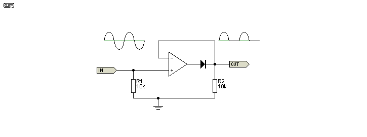
Figure 1 - Basic Precision Half Wave Rectifier
For a low frequency positive input signal, 100% negative feedback is applied when the diode conducts. The forward voltage is effectively removed by the feedback, and the inverting input follows the positive half of the input signal almost perfectly. When the input signal becomes negative, the opamp has no feedback at all, so the output pin of the opamp swings negative as far as it can. Assuming 15V supplies, that means perhaps -14V on the opamp output.
When the input signal becomes positive again, the opamp's output voltage will take a finite time to swing back to zero, then to forward bias the diode and produce an output. This time is determined by the opamp's slew rate, and even a very fast opamp will be limited to low frequencies - especially for low input levels. The test voltage for the waveforms shown was 20mV at 1kHz. Although the circuit does work very well, it is limited to relatively low frequencies (less than 10kHz) and only becomes acceptably linear above 10mV or so (opamp dependent).
Note the oscillation at the rectified output. This is (more or less) real, and was confirmed with an actual (as opposed to simulated) circuit. This is the result of the opamp becoming open-loop with negative inputs. In most cases it is not actually a problem. The large voltage swing is a problem though.
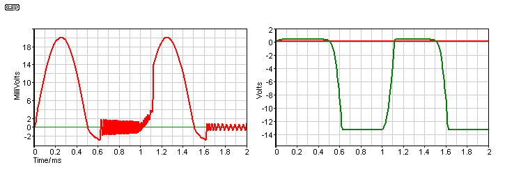
Figure 2 - Rectified Output and Opamp Output
Figure 2 shows the output waveform (left) and the waveform at the opamp output (right). The recovery time is obvious on the rectified signal, but the real source of the problem is quite apparent from the huge voltage swing before the diode. While this is of little consequence for high level signals, it causes considerable non-linearity for low levels, such as the 20mV signal used in these examples.
The circuit is improved by reconfiguration, as shown in Figure 3. The additional diode prevents the opamp's output from swinging to the negative supply rail, and low level linearity is improved dramatically. A 2mV (peak) signal is rectified with reasonably good accuracy. Although the opamp still operates open-loop at the point where the input swings from positive to negative or vice versa, the range is limited by the diode and resistor. Recovery time is therefore a great deal shorter.
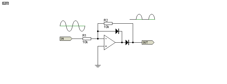
Figure 3 - Improved Precision Half Wave Rectifier
This circuit also has its limitations. The input impedance is now determined by the input resistor, and of course it is more complicated than the basic version. It must be driven from a low impedance source. Not quite as apparent, the Figure 3 circuit also has a defined output load resistance (equal to R2), so if this circuit were to be used for charging a capacitor, the cap will also discharge through R2. Although it would seem that the same problem exists with the simple version as well, R2 (in Figure 1) can actually be omitted, thus preventing capacitor discharge. Likewise, the input resistor (R1) shown in Figure 1 is also optional, and is needed only if there is no DC path to ground.
Figure 4 shows the standard full wave version of the precision rectifier. This circuit is very common, and is pretty much the textbook version. It has been around for a very long time now, and I would include a reference to it if I knew where it originated. The tolerance of R1, 2, 3, 4 and 5 are critical for good performance, and all five resistors should be 1% or better. Note that the diodes are connected to obtain a positive rectified signal. The second stage inverts the signal polarity. To obtain improved high frequency response, the resistor values should be reduced.
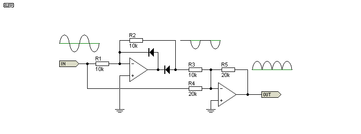
Figure 4 - Precision Full Wave Rectifier
This circuit is sensitive to source impedance, so it is important to ensure that it is driven from a low impedance, such as an opamp buffer stage. Input impedance as shown is 6.66k, and any additional series resistance at the input will cause errors in the output signal. The input impedance is linear. As shown, and using TL072 opamps, the circuit of Figure 4 has good linearity down to a couple of mV at low frequencies, but has a limited high frequency response. Use of high speed diodes, lower resistance values and faster opamps is recommended if you need greater sensitivity and/ or higher frequencies.
A little known variation of the full wave rectifier was published by Analog Devices, in Application Brief AB-109 [ 1 ]. In the original, a JFET was used as the rectifier for D2, although this is not necessary if a small amount of low level non-linearity is acceptable. The resistors marked with an asterisk (*) should be matched, although for normal use 1% tolerance will be acceptable. C1 may be needed to prevent oscillation.
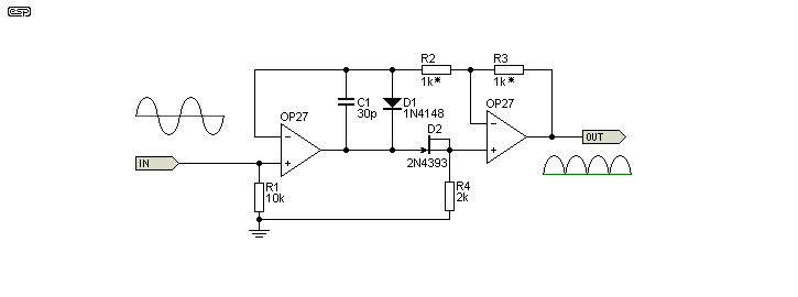
Figure 5 - Original Analog Devices Circuit
It was pointed out in the original application note that the forward voltage drop for D2 (the FET) must be less than that for D1, although no reason was given. As it turns out, this may make a difference for very low level signals, but appears to make little or no difference for sensible levels (above 20mV or so).
For most applications, the circuit shown in Figure 6 will be more than acceptable. Linearity is very good at 20mV, but speed is still limited by the opamp. To obtain the best high frequency performance use a very fast opamp and reduce the resistor values.

Figure 6 - Simplified Version of the AD Circuit
It is virtually impossible to make a full wave precision rectifier any simpler, and the circuit shown will satisfy the majority of low frequency applications. Where very low levels are to be rectified, it is recommended that the signal be amplified first. While the use of Schottky (or germanium) diodes will improve low level and/or high frequency performance, it is unreasonable to expect perfect linearity from any rectifier circuit at extremely low levels. Operation up to 100kHz or more is possible by using fast opamps and diodes. R1 is optional, and is only needed if the source is AC coupled, so extremely high input impedance (with no non-linearity) is possible. C1 may be needed to prevent oscillation.
The simplified version shown above (Figure 6) is also found in a Burr-Brown application note [ 3 ].
Purely by chance, I found the following variant in a phase meter circuit. This version is used in older SSL (Solid Stage Logic) mixers, as part of the phase correlation meter. This circuit exists on the Net in a few forum posts and a site where several SSL schematics are re-published. The original drawing I found is dated 1984. It's also referenced in a Burr-Brown paper from 1973 and an electronics engineering textbook [ 5, 6 ].
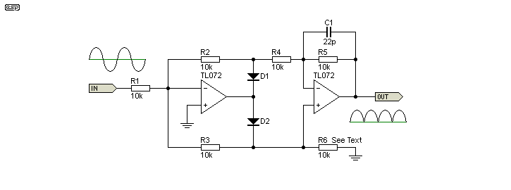
Figure 6A - Another Version of the AD Circuit
While it initially looks completely different, that's simply because of the way it's drawn (I copied the drawing layout of the original). This version is interesting, in that the input is not only inverting, but provides the opportunity for the rectifier to have gain. The inverting input is of no consequence (it is a full wave rectifier after all), but it does mean that the input impedance is lower than normal ... although you could make all resistor values higher of course. Input impedance is equal to the value of R1, and is linear as long as the opamp is working well within its limits.
R6 isn't used in the SSL circuit I have, and while the circuit works without it, there can be a significant difference between the rectified positive and negative parts of the input waveform. Without R6, the loading on D2 is less than that of D1, causing asymmetrical rectification. This resistor is included in the Figure 6 version, and the need for it was found as I was researching precision rectifiers for a project. It's not a problem with normal silicon small-signal diodes (e.g. 1N4148), but it becomes very important if you use germanium or Schottky diodes due to their higher leakage.
If R1 is made lower than R2-R5, the circuit has gain. If R1 is higher than R2-R5, the circuit can accept higher input voltages because it acts as an attenuator. For example, if R1 is 1k, the circuit has a gain of 10, and if 100k, the gain is 0.1 (an attenuation of 10). All normal opamp restrictions apply, so if a high gain is used frequency response will be affected. C1 is optional - you may need to include it if the circuit oscillates. The value will normally be between 10pF and 100pF, depending on the speed you need and circuit layout.
One interesting result of using the inverting topology is that the input node is a 'virtual earth' and it enables the circuit to sum multiple inputs. R1 can be duplicated to give another input, and this can be extended. The original SSL circuit used two of these rectifiers with four inputs each. Remember that this is the same as operating the first opamp with a gain of four, so high frequency response may be affected without you realising it.
The circuits shown in Figures 6 and 6A are the simplest high performance full wave rectifiers I've come across, and are the most suitable for general work with audio frequencies. In most applications, you'll see the Figure 4 circuit, because it's been around for a long time, and most designers know it well. However, it is definitely not the best performer, and has no advantages over the Figure 6 and 6A simpler alternatives, but it uses more parts and has a comparatively low input impedance.
I've been advised by a reader that Neve also used a similar circuit in their BA374 PPM drive circuit. In the interests of consistency I've shown the resistors (R1-R5 & R8) as 10k, where 51k was used in the original circuit. This doesn't change the way the circuit works, but it reduces resistive loading on the opamps (which doesn't affect low-frequency operation). The amended schematic is shown below.

Figure 6B - Neve PPM Rectifier Circuit
The R/C network (R6, R7 and C1) sets the ballistics of the meter, which is determined by the attack and release times. The output of the rectifier is processed further in the BA374 circuit to provide a logarithmic response which allows the meter scale to be linear. This isn't shown because it's not relevant here. Unfortunately, it's extremely difficult to determine who came up with the idea first. The Neve schematic I was sent is dated 1981 if that helps.
A simple precision rectifier circuit was published by Intersil [ 2 ]. This is an interesting variation, because it uses a single supply opamp but still gives full-wave rectification, with both input and output earth (ground) referenced. Unfortunately, the specified opamp is not especially common, although other devices could be used. The CA3140 is a reasonably fast opamp, having a slew rate of 7V/µs. I will leave it to the reader to determine suitable types (other than that suggested below). The essential features are that the two inputs must be able to operate at below zero volts (typically -0.5V), and the output must also include close to zero volts.
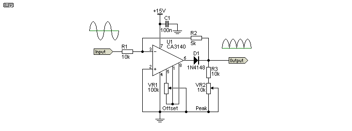
Figure 7 - Original Intersil Precision Rectifier Circuit
During the positive cycle of the input, the signal is directly fed through the feedback network to the output. R3 actually consists of R3 itself, plus the set value of VR2. The nominal value of the pair is 15k, and VR2 can be usually be dispensed with if precision resistors are used (R3 and VR2 are replaced by a single 15k resistor).
This gives a transfer function of ...
Gain = 1 / ( 1 + (( R1 + R2 ) / R3 )) ... 0.5 with the values shown above
1V input will therefore give an output voltage of 0.5V. During this positive half-cycle of the input, the diode disconnects the op-amp output, which is at (or near) zero volts. Note that the application note shows a different gain equation which is incorrect. The equation shown above works.
During a negative half-cycle of the input signal, the CA3140 functions as a normal inverting amplifier with a gain equal to -( R2 / R1 ) ... 0.5 as shown. Since the inverting input is a virtual earth point, during a negative input it remains at or very near to zero volts. When the two gain equations are equal, the full wave output is symmetrical. Note that the output is not buffered, so the output should be connected only to high impedance stage, with an impedance much higher than R3.
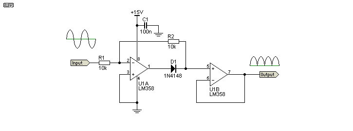
Figure 8 - Modified Intersil Circuit Using Common Opamp
Where a simple, low output impedance precision rectifier is needed for low frequency signals (up to perhaps 10kHz as an upper limit), the simplified version above will do the job nicely. It does require an input voltage of at least 100mV because there is no DC offset compensation. Expect around 30mV DC at the output with no signal. Because the LM358 is a dual opamp, the second half can be used as a buffer, providing a low output impedance. The second half of the opamp can be used as an amplifier if you need more signal level. Minimum suggested input voltage is around 100mV peak (71mV RMS), which will give an average output voltage of 73mV. Higher input voltages will provide greater accuracy, but the maximum is a little under 10V RMS with a 15V DC supply as shown. The LM358 is not especially fast, but is readily available at low cost.
Limitations: Note that the input impedance of this rectifier topology is non-linear. The impedance presented to the driving circuit is very high for positive half cycles, but only 10k for negative half-cycles. This means that it must be driven from a low impedance source - typically another opamp. This increases the overall complexity of the final circuit. Note that symmetry can be improved by changing the value of R3. It can be made adjustable by using a 20k trimpot (preferably multi-turn). This isn't necessary unless your input voltage is less than 100mV, and the optimum setting depends on the signal voltage.
An interesting variation was shown in a Burr-Brown application note [ 3 ]. This rectifier operates from a single supply, but accepts a normal earth (ground) referenced AC input. The only restriction is that the incoming peak AC signal must be below the supply voltage (typically +5V for the OPA2337 or OPA2340). The opamps used must be rail-to-rail, and the inputs must also accept a zero volt signal without causing the opamp to lose control.
The circuit is interesting for a number of reasons, not the least being that it uses a completely different approach from most of the others shown. The rectifier is not in the main feedback loop like all the others shown, but uses an ideal diode (created by U1B and D1) at the non-inverting input, and this is outside the feedback loop.
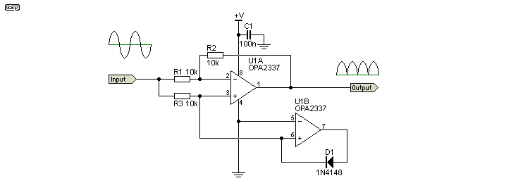
Figure 9 - Burr-Brown Circuit Using Suggested Opamp
For a positive-going input signal, the opamp (U1A) can only function as a unity gain buffer, since both inputs are driven positive. Both the non-inverting and inverting inputs have an identical signal, a condition that can only be achieved if the output is also identical. If the output signal attempted to differ, that would cause an offset at the inverting input which the opamp will correct. It is worth remembering my opamp rules described at the beginning of this app. note.
For a negative-going input signal, The ideal diode (D1 and U2B) prevents the non-inverting input from being pulled below zero volts. Should this happen, the opamp can no longer function normally, because input voltages are outside normal operating conditions. The opamp (U1A) now functions as a unity gain inverting buffer, with the inverting input maintained at zero volts by the feedback loop. If -10µA flows in R1, the opamp will ensure that +10uA flows through R2, thereby maintaining the inverting input at 0V as required.
Limitations: Input impedance is non-linear, having an almost infinite impedance for positive half-cycles, and a 5k input impedance for negative half-cycles. The input must be driven from an earth (ground) referenced low impedance source. Capacitor coupled sources are especially problematical, because of the widely differing impedances for positive and negative going signals. The maximum source resistance for a capacitor-coupled signal input is 100 ohms for the circuit as shown (one hundredth of the resistor values used for the circuit), and preferably less. The capacitance is selected for the lowest frequency of interest.
This rectifier is something of an oddity, in that it is not really a precision rectifier, but it is full wave. It is an interesting circuit - sufficiently so that it warranted inclusion even if no-one ever uses it. This rectifier was used as part of an oscillator [ 4 ] and is interesting because of its apparent simplicity and wide bandwidth even with rather pedestrian opamps.
A simulation using TL072 opamps indicates that even with a tiny 5mV peak input signal (3.5mV RMS) the frequency response extends well past 10kHz but for low level signals serious amplitude non-linearity can be seen. The original article didn't even mention the rectifier, and no details were given at all. However, I have been able to determine the strengths and weaknesses by simulation. Additional weaknesses may show up in use of course. A reader has since pointed out something I should have seen (but obviously did not) - R3 should not be installed. Without R3, linearity is far better than expected.
It's not known why R3 was included in the original JLH design, but in the case of an oscillator stabilisation circuit it's a moot point. The circuit will always have more or less the same input voltage, and voltage non-linearity isn't a problem.

Figure 10 - Simple Precision Full Wave Rectifier
One thing that is absolutely critical to the sensible operation of the circuit at low signal levels is that all diodes must be matched, and in excellent thermal contact with each other. The actual forward voltage of the diodes doesn't matter, but all must be identical. The lower signal level limit is determined by how well you match the diodes and how well they track each other with temperature changes.
The first stage allows the rectifier to have a high input impedance (R1 is 10k as an example only). Nominal gain as shown is 1 (with R3 shorted). R3 was included in the original circuit, but is actually a really bad idea, as it ruins the circuit's linearity. Without it, the circuit is very linear over a 60dB range. This is more than enough for any analogue measurement system.
Limitations: Linearity is very good, but the circuit requires closely matched diodes for low level use because the diode voltage drops in the first stage (D1 & D2) are used to offset the voltage drops of D3 & D4. At input voltages of more than a volt or so, the non-linearities are unlikely to cause a problem, but diode matching is still essential (IMO). Low level performance will be woeful if accurate diode forward voltage and temperature matching aren't up to scratch. A forward voltage difference of only 10mV between any two diodes will create an unacceptable error. The overall linearity is considerably worse if R3 is included.
Simple capacitor smoothing cannot be used at the output because the output is direct from an opamp, so a separate integrator is needed to get a smooth DC output. This applies to most of the other circuits shown here as well and isn't a serious limitation.
The final circuit is a precision full-wave rectifier, but unlike the others shown it is specifically designed to drive a moving coil meter movement. There is no output voltage as such, but the circuit rectifies the incoming signal and converts it to a current to drive the meter. This general arrangement is (or was) extremely common, and could be found in audio millivoltmeters, distortion analysers, VU meters, and anywhere else where an AC voltage needed to be displayed on a moving coil meter. Digital meters have replaced it in most cases, but it's still useful, and there are some places where a moving coil meter is the best display for the purpose. This type of rectifier circuit is discussed in greater detail in AN002.
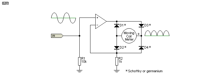
Figure 11 - Moving Coil Meter Amplifier
The circuit is a voltage to current converter, and with R2 as 1k as shown, the current is 1mA/V. If a 1V RMS sinewave is applied to the input, the meter will read the average, which is 900µA. Adjusting R2 varies the sensitivity, and changing R2 to 900 ohms means the meter will show 1mA for each volt (RMS) at the input. This assumes a meter with a reasonably low resistance coil, although in theory the circuit will compensate for any series resistance.
This type of circuit almost always has R2 made up from a fixed value and a trimpot, so the meter can be calibrated. Although shown with an opamp IC, the amplifying circuit will often be discrete so that it can drive as much current as needed, as well as having a wide enough bandwidth for the purpose. Millivoltmeters and distortion analysers in particular often need an extended response (100kHz or more is common), and few opamp ICs are able to provide a wide enough bandwidth to work well with anything much over 15kHz. The problem is worse at low levels because the opamp output has to swing very quickly to overcome the diode forward voltage drop. It's common to use a capacitor in parallel with the movement to provide damping, but that also changes the calibration.
Limitations: The output is very high impedance, so the meter movement is not damped unless a capacitor is used in parallel. The meter will then show the peak value which might not be desirable, depending on the application.
As already noted, the opamp needs to be very fast. Linearity is good provided the amplifier used has high bandwidth. The circuit works better with low-threshold diodes (Schottky or germanium for example), which do not need to be matched because the circuit relies on current, and not voltage. It also only works as intended with a moving coil meter and is not suited to driving digital panel meters or other electronic circuits. It can be done, but there's no point as the circuit would be far more complex than others shown here.
Although the waveforms and tests described above were simulated, the Figure 6 circuit was built on my opamp test board. This board uses LM1458s - very slow and extremely ordinary opamps, but the circuit operated with very good linearity from below 20mV up to 2V RMS, and at all levels worked flawlessly up to 35kHz using 1k resistors throughout. Variations of Figure 11 have been used in several published projects and in test equipment I've built over the years. While most of the circuits show standard signal-level diodes (e.g. 1N4148 or similar), most circuits perform better with Schottky diodes, and even germanium diodes can be used with some of the circuits. These both have the advantage of a lower forward voltage drop, but they have higher reverse leakage current which may cause problems in some cases.
One thing that became very apparent is that the Figure 6 circuit is very intolerant of stray capacitance, including capacitive loading at the output. Construction is therefore fairly critical, although adding a small cap (as shown in Figures 5 & 6) will help to some extent. I don't know why this circuit has not overtaken the 'standard' version in Figure 4, but that standard implementation still seems to be the default, despite its many limitations. Chief among these are the number of parts and the requirement for a low impedance source, which typically means another opamp. The impedance limitation does not exist in the alternative version, and it is far simpler.
The Intersil and Burr-Brown alternatives are useful, but both have low (and non-linear) input impedance. They do have the advantage of using a single supply, making both more suitable for battery operated equipment or along with logic circuitry. Remember that all versions (Figures 7, 8 & 9) must be driven from a low impedance source, and the Figure 7 circuit must also be followed by a buffer because it has a high output impedance.
In all, the Figure 6 circuit is the most useful. It is simple, has a very high (and linear) input impedance, low output impedance, and good linearity within the frequency limits of the opamps. The Figure 6A version is also useful, but has a lower input impedance and requires 2 additional resistors (R1 in Figure 6 is not needed if the signal is earth referenced).
The above circuits show just how many different circuits can be applied to perform (essentially) the same task. Each has advantages and limitations, and it is the responsibility of the designer to choose the topology that best suits the application. Not shown here, but just as real and important, is a software version. Digital signal processors (DSPs) are capable of rectification, conversion to RMS and almost anything else you may want to achieve, but are only applicable in a predominantly digital system.
With all of these circuits, it's unrealistic to expect more than 50dB of dynamic range with good linearity. This gives a range from 10mV up to 3.2V (peak or RMS) with supplies of ±12-15V. Use of precision high speed opamps may increase that, but if displayed on an analogue (moving coil) meter, you can't read that much range anyway - even reading 40dB is difficult. 100:1 (full scale to minimum) is not easily read on most analogue movements - even assuming that the movement itself is linear at 100th of its nominal FSD current.
Many of the circuits shown have low impedance outputs, so the output waveform can be averaged using a resistor and capacitor filter. The value appearing across the filter cap is the average of the rectified signal - for a sinewave, the average is calculated by ...
VAVG = ( 2 × VPeak ) / π or ...
VAVG = VPeak × 0.637
It turns out that the RMS value of a sinewave is (close enough to) the average value times 1.11 (the inverse is 0.9) and this makes it easy enough to convert one to another. However, it only gives an accurate reading with a sinewave, and will show serious errors with more complex waveforms. To see just how much error is involved, see AN012 which covers true RMS conversion techniques and includes a table showing the error with non-sinusoidal waveforms.
 Main Index
 App. Notes Index