

|
| Elliott Sound Products | Project 213 |
 Main Index Main Index
 Projects Index Projects Index
|
VCAs (voltage controlled amplifiers/ attenuators) are a special case in electronics. There are several possible ways they can be made, but most are not linear. This applies either to the voltage control itself, or the distortion created by simple circuits (or both). One of the better solutions is an LED/ LDR optocoupler, which can provide very good distortion figures, but they have control characteristics that are at best a lottery. The control system is unpredictable, due to both the LED and the LDR (light dependent resistor). It may be possible to match individual units to get a usable result, but mostly it's close to impossible.
Before going much further, I suggest that you read the VCA Techniques article. There are many different ways to make a VCA, but most are unsuitable for DIY construction because they require tightly matched components. The IC versions are particularly hard - rumour has it that people have made Blackmer VCA blocks with discrete parts, but I've not seen one published anywhere. BJTs (bipolar junction transistors) work surprisingly well, provided the input level is kept 'reasonable' (which in this context means no more than 500mV RMS).
The version shown in the VCA Techniques article uses a current mirror as the load for the long-tail pair (LTP). I opted to use a simple resistive load instead, not just to reduce the parts cost, but to make the circuit simpler. A current mirror load requires closely matched transistors, and that would make construction more difficult. The mirror also needs some form of offset correction, something that's optional with resistor loads.
The circuit described here makes no claims for 'superb audio performance', it's utilitarian, and quite good fun to build and play with. That was my goal - not to try to present something that no-one can put together, but an educational circuit that's also practical for use. It's been simulated, but more importantly, it's also been fully bench tested. I quite deliberately didn't match the transistors for VBE or β (beta - gain, aka hFE), but just installed them as they came out of their bag. I built a stereo version, so I could see how much variation existed between the two without any form of trimming. I was pleasantly surprised, both by the distortion performance, noise and tracking between the two.
There used to be a number of different 'OTAs' (operational transconductance amplifiers), with the CA3280 and LM13600/ LM13700 being common, but most disappeared a few years ago. Interestingly, the LM13700 is currently listed as active, and is available from several suppliers. A couple list it as 'end of life', and you may only be able to get it in a SOIC (SMD) package. I don't have any, so I can't make comparisons with the design shown here. I'd expect them to be fairly similar, but the DIY version may marginally better.
The circuit is very similar to the one shown in the 'VCA Techniques' article, but is slightly simpler. Each channel uses four transistors and one opamp, plus the obligatory resistors and capacitors of course. Not surprisingly, I used Veroboard for the one I built, and it's been tested with music, and an audio signal generator for distortion and frequency response tests. The frequency is good up to at least 100kHz, and the bottom end is 3dB down at 7Hz with the values I used.
To ensure that the opamp can function properly, the VCA section is run from a separate +5V supply. This needs to be quiet, or noise will be injected into the LTP (long-tailed pair). In theory it will be cancelled out by the differential input to the opamp, but reality (and Murphy's law) will indicate otherwise. My prototype doesn't include the filter, as I wanted a 'worst case' test unit. It turned out to be surprisingly quiet, even at maximum gain.
Note that the 0-10V control voltage is indicative only. It can be changed at will, and during some of my tests I used 0-12V. A higher control voltage will give a correspondingly higher gain with the CV limiting resistor (R7) left at 10k. Likewise, reducing the value of R7 increases the maximum gain, but control voltage feedthrough will increase significantly. Somewhere between 0-10V and 0-12V with the recommended resistance is close to optimum. There is a 'dead-spot' at the lowest voltages. No current can flow until the voltage at the base of Q3/Q4 reaches 500mV, and the input current to Q3/Q4 ranges from 10µA to 930µA over the operating range.
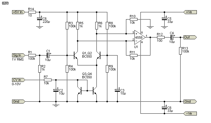
The control voltage is from zero to +10V, which provides a minimum gain of zero (maximum attenuation) and a maximum of 3.18 (10dB) with the values shown. The maximum input voltage recommended is 1V RMS, but distortion is reduced with lower levels. Before the VCA itself, the input is attenuated by 100 (101 to be precise), so 1V input is reduced to 10mV. It's most unfortunate that the input level is so low, but distortion increases rapidly with any more. According to the simulator, the distortion with 1V input is about 0.54%, which is far greater than would normally be considered acceptable. Reducing the distortion requires far greater complexity, and it becomes almost impossible to match transistors closely enough to get a good result.
In theory, adding emitter resistors to the two LTP transistors may improve linearity, but in practice it appears to make little or no worthwhile difference. Up to about 22Ω can be used, which will reduce distortion, but at the expense of control linearity. In the test version I built, I didn't include the resistors, and distortion was measured at around 0.08% with 250mV RMS input. Even with zero transistor matching, the two VCAs tracked to within 1dB, and that can be improved by adding a trimpot in series with the control voltage input. Once the gain is matched at the nominal output level (say 500mV RMS), the two VCAs tracked almost perfectly (within 0.5dB over the full range). The distortion performance is shown in Fig. 8.
There is some control voltage (CV) feedthrough, so it's not suitable anywhere that the gain is changed rapidly. For controlling volume (for example) this will not be an issue, but it may cause problems in fast acting limiters or anywhere else where the gain is changed quickly. A pot (around 100Ω) can be used to balance Q1 and Q2, and the wiper goes to the +5V supply, with one end to R5 and the other to R6. The pot is adjusted for minimum CV feedthrough. I didn't include this on my prototype, but the full circuit is shown in Figure 3.
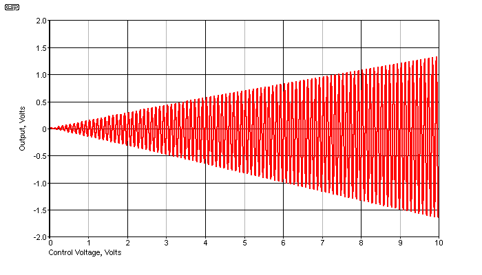
The level shift is visible in the above graph. The positive peaks reach +1.3V, and the negative peaks are at -1.645, indicating an offset of about -144mV. The output capacitor removes this of course, but any rapid transition will get through and be potentially audible (depending on how the VCA is used). You can use the Figure 3A version if you want to improve the CV rejection. After initial tests I added balancing pots for Q1 and Q2. They helped, but were not a resounding success because I didn't match the transistors.
The linearity of output vs. control voltage is very good, which is an important factor for multi-unit tracking. As shown, the control voltage used a perfectly linear ramp generator (in the simulator), varying from zero to 10V. The control current is therefore from zero to ~935µA, and this is mirrored by Q4, controlling the tail current of the LTP. They will never be equal, even if the transistors are perfectly matched, as the current mirror is only basic. For this application, there is no point making it any more complex.
The input level was 500mV RMS (707mV peak), resulting in a distortion of about 0.18%. The maximum gain is just over two (6dB), but this can be increased by increasing the value of R10 and R11. This has no effect on distortion, but it will increase the maximum control voltage feedthrough. Note that the output capacitor (C4) is wired to allow for the slightly negative output voltage at maximum gain. If these resistors are changed to 22k, the maximum gain will be around 4.6 (a little over 13dB). You can also change the gain range by varying the control voltage limiting resistor (R7, which acts as a voltage-to-current converter). See below for suitable warnings on this though - the value shown is close to ideal.

The version shown above includes the available techniques to balance the control voltage and reduce distortion. The two diodes act as 'pre-distortion' devices, and they help to lower the distortion, particularly at higher input (signal) voltages. The diodes can reduce the distortion from around 0.54% to 0.34% with 1V RMS input, or from 0.057% down to 0.04% with 250mV input. It's up to the constructor to decide if that provides a worthwhile benefit for the application. Note that these results were simulated, but the simulation on the Figure 1 circuit agreed almost perfectly with the unit I built, so the results are probably trustworthy.
The value of R3 may need to be altered depending on the diodes (which should be matched if you match Q1 and Q2). This is something that the constructor can play with, but the value shown (15k) seems about right. Note that the values of R2, R4 and R9 are also changed, and the maximum gain is a little lower. Personally, I don't think it's worth the extra parts, but I leave that to you.
I mentioned above that there is enough control voltage (CV) feedthrough on the Fig. 1 circuit to make it unusable if there's a fast change in the CV. This will happen if the circuit were to be used as a compressor or limiter for example, or if it's used as a modulator for an AM transmitter - assuming that the opamp can handle the carrier frequency (typically 535-1,605 kHz). This is a big ask for any opamp. However, if you need the minimum CV feedthrough, use the following circuit.
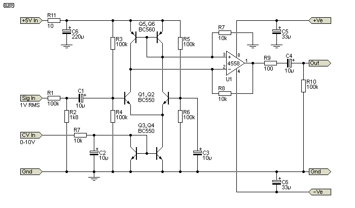
Using a current mirror instead of the resistors makes a big difference to CV breakthrough, but has no effect on the overall linearity. Unless you plan to use rapid CV changes, there's no advantage to adding the mirror. To really minimise CV breakthrough, you will need to match the transistors for the LTP (long-tailed pair) and the upper current mirror. Matching is only required between Q1 and Q2, with Q5 and Q6 also matched. There is no requirement to match the NPN and PNP devices, which would be virtually impossible anyway. Note that all measurements were taken with the Fig. 1 circuit, and not the version shown here.
Of course, one of the questions that will inevitably arise is "How does it work?". The gain of the LTP is determined by the 'tail' current. When it's low (say 50µA), it's obvious that the current through Q1 and Q2 is only 25µA. Increase the tail current to 500µA, and each transistor will have a collector current of 250µA. Gain control makes use of the fact that a transistor's signal gain can be varied by changing the emitter current. This is largely due to the intrinsic (internal) emitter resistance, commonly known (literally) as 'little r-e' (re). The accepted value is determined by ...
re = 26 / Ie (in milliamps)
With an emitter current of 25µA, re will be around 1MΩ, falling to 104k at 250µA. Naturally, as the value of re changes, so too does the transistor's gain. Because the current through each transistor only varies by a small amount due to the signal, distortion is fairly low and primarily second order. Because the opamp is connected differentially, most of the 2nd harmonic distortion is cancelled, With a 1V CV signal, the transistors have a gain of 0.38 (i.e. a loss), and with 5V the gain is 3.94. Thus, by altering the tail current, the transconductance of Q1 and Q2 is changed, changing the gain. While a full analysis might be enjoyed by some readers, I expect that most will be happy enough with the very simplified version shown - it rapidly descends into serious maths to delve any deeper. The opamp is used to sum the two outputs in differential mode, so the output from both transistors is used.
The two transistors in the LTP 'talk' to each other via their emitters (note the Q2 has its base grounded for AC). The impedance of a current source is very high (not quite infinite, but at least several megohms), and little or no emitter signal is 'lost' via the current source. If the internal emitter resistance changes, so too does the collector signal for both transistors. The information available on the Net is not especially useful on this point, even though it's a technique that's been around for a long time. All common amplifying devices (BJTs, JFETs, MOSFETs and valves [vacuum tubes]) show the same effect.
All devices were simulated (BJTs, JFETs, MOSFETs and a 12AU7), and all provided variable gain. Interestingly, the BJT is the only device that is capable of an almost perfectly linear amplitude response as the control (tail) current changes, as shown in Figure 2. All other devices increased their gain more rapidly at low tail currents, and it tapered off as the maximum was approached.
Distortion is always an important parameter, so I took some measurements. I measured the output from the distortion meter, and also ran the FFT (fast Fourier transform) function to look at the output frequencies. There is no point showing the waveform itself, as no oscilloscope has the resolution to let you see distortion below 1% or so (and even that can be hard in many cases).

Since this is from the output of my distortion meter, so the fundamental (400Hz) is removed, leaving only distortion and noise. The distortion is interesting. Unlike most circuitry, distortion is limited to second and third harmonics, with almost nothing beyond that. With 400Hz input, there's a peak at 800Hz (2nd harmonic) and another at 1,200Hz (3rd harmonic), and what remains is buried in noise. This matches the simulation almost perfectly. The waveform is notable in that it's quite smooth, which indicates that there are no higher order harmonics at all (they show up as sharp discontinuities on top of the lower frequencies you can see).
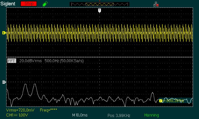
Using the scope's FFT function, you can see the two harmonics, and they are almost exactly the same amplitude. If a 'balance' pot is used with the collector resistors for Q1 and Q2, the 2nd harmonic is suppressed a bit more, but not enough to be significant (the measured THD changes very little).
Note that the circuit shown has no temperature compensation, so the gain will vary slightly with temperature. It's not intended to be a precision circuit, and the added complexity would take it out of the realm of 'simple' DIY. In normal usage, the transistor temperatures will be almost identical (at room temperature) as dissipation is very low so there's no self-heating. The maximum dissipation in any of the transistors will be less than 2mW at any setting.
Alternately, you can get a good result from JFETs, and while distortion is lower, the overall gain is also lower and the control is not linear. JFETs also have a wide parameter spread, so it can be difficult to get a well matched pair. While matched pairs are available from Linear Systems (e.g. LSK389), they are not inexpensive. The JFET version is shown below, and has been simulated but not bench tested.
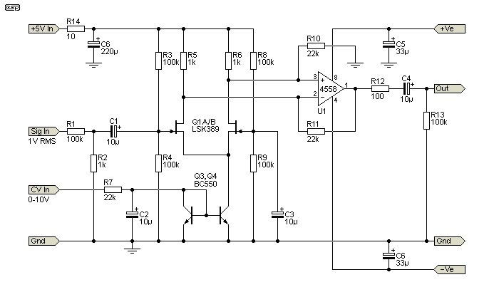
Using JFETs means that the overall gain is reduced to about half that of BJTs. The control curve is non-linear as well, and while it's possible to modify the 'law' of the control pot, you probably wouldn't bother. It's probable that you should be able to reduce distortion to less than 0.01% using matched JFETs, but the cost may be such that it would be cheaper to use a THAT2181 or similar, which will give better performance overall. However, these VCAs have a logarithmic control function (typically around 6mV/ dB), and this may not be suitable for some circuits.
This is more of an educational project than anything else, but it can be used to advantage in relatively undemanding applications. The distortion is too high for it to qualify as hi-if, even though it's far better than some valve (vacuum tube) amplifiers that some people seem to like. The distortion is low-order, showing only second and third harmonics at any level above -100dB referred to 1V. Using only cheap parts, it's an easy way to play with a 'true' VCA for minimal outlay.
As noted, Q1 and Q2 will ideally be matched. It used to be common to obtain dual matched pairs in a single package, but most available now are SMD only, which makes it hard for DIY. This is especially true if you use Veroboard, as there is no easy way to connect SMD parts. While some through-hole types are still available, 'frighteningly expensive' doesn't come close when discussing the cost. This is not an acceptable path for a cheap DIY 'fun' project!
Noise is surprisingly low, and was inaudible through my workshop system until I was only 100mm from the speaker. I was pleasantly surprised, especially as I didn't include any filtering after the 78L05 regulator I used to generate the 5V supply to the LTP.
Nothing is critical in construction, and most of the circuitry is low impedance and has minimal hum pickup.
 |
The photo also shows the location of inputs, outputs, DC and ground. The piece of Veroboard I used was an offcut that just happened to be big enough for everything to fit (I modified the photo to remove 'dead space' to the right of the opamp). The VCAs are mirror images, with the dual opamp in between the two. The 5V regulator feeds both sets of transistors. The various parts of the circuit should be fairly recognisable from the schematic. DC power connections are just to the right of the opamp, as I originally planned to only make one VCA. The second was added so I could compare them for tracking. Neither had provision for balancing the LTP, but that was added later (the two blue trimpots). I cheated with these, as they are 1k trimpots, so the collector resistors are effectively 1,500Ω. This makes almost no difference to the circuit's operation.
The only parts missing from the board are the opamp output caps and resistors (C4 and R13). All tests I ran used the circuit DC coupled from the outputs, using the resistor leads from Pin 1 and Pin 7 as connection points. Resistor leads were also used for the signal input (top left and right) and the control voltage (bottom left and right).
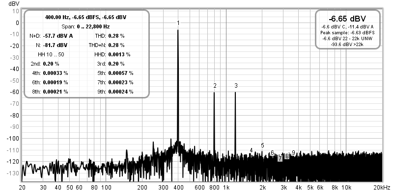
I used the Project 232 distortion measurement system to provide a better insight into the circuit's performance. The system says THD+N (distortion plus noise) is 0.28%, with noise at -82dB (near enough). Considering that the input signal is attenuated by ×100 before it even gets to the VCA indicates that the circuit itself is surprisingly quiet. It's not as good as a mid-range opamp, but for a simple (and very cheap) VCA it's much better than I expected.
Apart from the obvious fun of putting something like this together and playing around with it, the VCA is ideally suited for a guitar tremolo (amplitude modulation). Unlike a LED/ LDR combination, the tremolo depth doesn't change with frequency, and it's very linear. Note that amplitude modulation is tremolo, and frequency modulation is vibrato. The 'tremolo arm' on Fender guitars is incorrectly named - it causes vibrato not tremolo. Likewise, Fender amps claiming 'vibrato' provide tremolo. The maximum tremolo frequency used by most guitarists is around 15Hz (beyond that it starts to sound really weird), but the circuit will work with anything up to around 100Hz - almost certainly not useful, but it might be 'interesting'. Naturally, the modulating waveform needs to have a suitable DC offset to provide some gain. For example, close to 100% modulation is obtained with a 4V peak sinewave superimposed on a 5V DC level. CV feedthrough becomes audible above 30Hz, but that's much too high for tremolo circuits.
There are any number of applications for a VCA, but if you want to use them for hi-fi volume control, you're much better off with something like the Project 141 VCA Preamplifier. The circuits described here are primarily for the fun of it (and yes, I did have fun playing around with different effects). More importantly, it's educational to put something like this together and see how it works for yourself.
Should anyone think of complaining that I didn't go far enough with improvements, that's quite deliberate. As stated in the intro, any DIY circuit has to be simple (and cheap) enough that anyone can build it, and mess around with the result to see what happens. It can be used in a real circuit, provided you don't expect miracles. I certainly wouldn't use it for hi-if, but as a guitar tremolo modulator or as a simple VCA intended to maintain a preset background audio level (with a rectifier and filter to generate a control voltage), it should do very nicely.
As you can see from the distortion performance shown in Fig. 8, it's far better than you would expect for something that costs less than $5 in parts. It's not hi-if, but it is more than acceptable for casual listening, and I expect that
There are quite a few similar VCA circuits on the Net, but most (well, none that I saw) use a current mirror to control the LTP tail current. This circuit was devised using basic principles, and no specific references are shown, as none were used to create the circuit.
One useful site (found when this article was almost finished, and which includes all formulae) is on the Analog Devices website - see Chapter 12: Differential Amplifiers, which is part of the AD 'University' series. While the explanations are mainly pretty good, I believe there are errors in the formulae presented (I could also be wrong).
 Main Index Main Index
 Projects Index Projects Index
|