
|
|
| Elliott Sound Products | Project 15 |
Since I have provided the schematic for John L Linsley-Hood's Class-A amplifier and the ESP derivative called 'Death of Zen' (DoZ), I felt that some readers may wish to experiment with the concept of capacitance multipliers. Unfortunately, a very low ripple power supply is needed for many Class-A amps, and the most common solution is to use a regulated supply. A basic circuit is provided in the article, but it is assumed that the builder knows all the pitfalls. The supplied JLL-Hood schematic is in fact for a capacitance multiplier filter (not a regulator), but the description and determination of component values is somewhat lacking (I feel) and can be improved.
This class of circuit has been called a 'capacitance multiplier' for decades, but it's really no such thing. See Capacitance Multiplier Power Supplies for some more design details and an explanation of the terminology. There is no multiplication of the capacitance in the circuit, and it's actually a buffered filter with the buffer providing the output current.
| WARNING: Because this power supply is mains operated, there is the risk of electrocution if extreme care is not exercised while constructing or testing the unit. If you are not confident in your abilities with mains powered equipment, do not attempt construction under any circumstances .... please! |
While the performance of a true regulated supply will usually be excellent (if properly designed and built), there are a number of problems for a high-current, low ripple design if regulators are used. Two of the main ones are:
For the sake of the exercise, assume that we want the following specifications:
These specifications are typical, since Britain, Europe and Australia use nominal 230V mains, but the voltages can easily be scaled for the US 120V mains supply. All are subject to variations, both long and short term.
We are not actually all that interested in the mains input voltage, only the possible variations of the output of the transformer/ rectifier/ filter combination.
For a regulated output of 20 Volts, we need a minimum input voltage of about 23 Volts, since most regulator circuits have a 'dropout' voltage, below which they cannot regulate. This voltage is the absolute minimum, including the mains ripple which will be superimposed on the DC (See Fig 1). Note that for all calculations I am assuming 50Hz mains supply. The results will be slightly different for 60Hz (as used in the US), but are not significant.
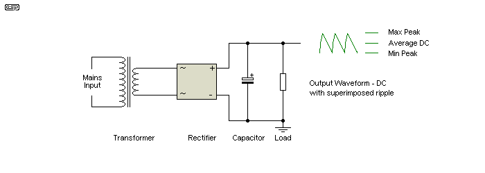
Figure 1 - Basic Rectifier
Once the regulator's input voltage drops below the dropout voltage, regulation will naturally fail, and ripple will appear at the output. This will eventually find its way to our ears, causing much muttering and complaining, and rude words surely cannot be far behind!
We must assume that the transformer / rectifier / filter will have a regulation in the order of 10% (this is fairly typical for a full-wave bridge rectifier). Using the normal 1.414 RMS to peak conversion (the square root of 2), plus a few assumptions based on experience, we therefore have our minimum requirement:-
This will provide a no load voltage of about 23.5 Volts as expected. When loaded to about 2.5 Amps, this will change:
These figures were simulated, but reality will be suspiciously close!
It can be readily seen that far more voltage is needed to ensure that the minimum voltage of 23 Volts is maintained. It turns out (again from my trusty simulator) that a transformer voltage of 22 V RMS is needed, which provides an average DC of 25.4 Volts, less about 2 Volts peak ripple. Close enough.
Now comes the really nasty bit! All of the above must be the case at the lowest possible mains voltage. For the sake of (my) sanity, this is assumed to be 200 V AC, so at the above worst case maximum of 260V, the 22V output of the transformer is now 28.6V. At full load (2.5A), this yields a DC voltage of nearly 35V average.
So the regulator will have a minimum input voltage of 25.4 Volts, and a maximum of 35V, so power dissipation will be:
Note that the above figures are for the 1.25A average, but peak dissipation (at 2.5A) will be double, at about 37W for the worst case. This is a lot of heat to dispose of, and must be catered for. I should also mention that a minimum of 200V AC for a nominal 230V may be optimistic (10% of 230V is 23V) and in reality we may need to cater for even lower voltages. This makes the equation even worse!
To accommodate the worst case, the heatsink for the power supply must be capable of ensuring the maximum device temperature is not exceeded at the highest mains voltage anticipated. At no 'normal' mains voltage may the regulator come out of regulation, or severe ripple will appear at the output, degrading the sound quality, and causing audible hum (at double the mains frequency, and with a triangular waveshape, which sounds horrid).
The only real thing to worry about is the degree of filtering needed! We must assume that up to 3 Volts may be lost across the capacitance-multiplier filter, to ensure that the DC input (including ripple component) always exceeds the output voltage. Transient performance may also need to be considered if the load current is not continuous. In general, the minimum differential voltage from input to output should be no less than 1-2 volts (based on the lowest point of the input ripple).
Because there is no regulation, the power amplifier must be capable of accepting the voltage variations from the mains - every standard power amplifier in existence does this quite happily now, so it is obviously not a problem. Note that the output power is affected, but this happens with all amps, and cannot be avoided without a regulator.
We can now design for nominal mains voltage (say 220V AC), and with very simple circuitry, provide a filter which will dissipate no more than about 4 Watts in normal use - regardless of mains voltage. Figure 2 shows the basic configuration of a capacitance-multiplier filter, which is actually a buffered filter. The capacitance is not 'multiplied', only the current through the base feed resistor (or resistors). Because the base is a relatively high impedance, the amount of capacitance is reduced for a given ripple reduction. The base current is in milliamps rather than amps, assuming a gain of 1000 in the output device.
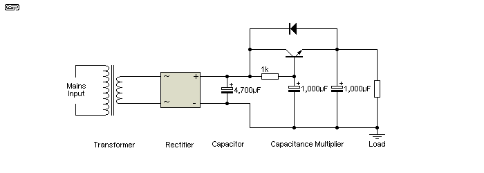
Figure 2 - Single (Basic) Capacitance Multiplier
One could simply use a pair of 1F caps for a dual supply, but I have noticed a dearth of such devices (other than the 5V 'Super Capacitors' used for memory backup in computers or the massive caps often used with car power amps). Since they will need to be rated at about 35V, and be capable of considerable ripple current, I cannot help but feel that this is not a viable option.
Both methods will provide a ripple of well under 5mV RMS, but the multiplier has the advantage of removing the triangular waveform - it is not a sinewave, but has a much lower harmonic content than would be the case even with a 1F capacitor.
To obtain a gain of 1,000 for a power transistor, we need to use a Darlington - either an encapsulated Darlington device, or a pair of 'ordinary' transistors connected in a Darlington pair (See Figure 3). The latter method is my preferred option, since it allows greater flexibility in obtaining devices, and will often have better performance. Another alternative is to use a complementary feedback (Sziklai) pair, as shown in Figure 4. Interestingly, the complementary circuit not only reduces dissipation, but may also provide marginally better performance in terms of hum filtering.
The simple capacitance multiplier filter described above is quite satisfactory as a starting point, but its operating characteristics are too dependent on the gain of the output transistor(s). What is needed is a circuit whose performance is determined by resistors and capacitors, and which is relatively independent of active devices (although these will still have an impact on the degree of filtering provided).
We can also improve the ripple rejection, and the final circuit for a dual supply is shown in Figure 3. This circuit reduces ripple to less than 1mV with typical devices (about 250uV RMS as simulated), and dissipates less than 4 Watts per output transistor at 1.25A continuous operating current. It is unlikely that you will achieve this low hum level in practice, since real wire has resistance. However, with careful layout you should easily be able to keep the output hum and noise to less than 10mV, and this level is more than acceptable for any power amp application.
By splitting the capacitance with an additional resistor, we create a second order filter (12dB/octave rolloff), which reduces the hum more effectively, and also removes more of the higher order harmonics (which tend to make a 'hum' into a 'buzz' - much more audible and objectionable). The resistor to ground stabilises the circuit against variations in transistor gain, but increases dissipation slightly. This is done deliberately to ensure that there is sufficient voltage across the multiplier to allow for short term variations.
The 12k resistor shown may need to be adjusted to suit your transistors and supply voltage. Reducing the value increases dissipation in the output devices and lowers output voltage. It is unlikely that any benefit will be obtained by increasing this resistor, but you may experience increased hum (hardly a benefit).

Figure 3 - Complete Dual Capacitance Multiplier (Darlington Pair)
This is an easy design to build, but requires great care to ensure that ripple currents are not superimposed on the output because of bad grounding or power wiring practices. The schematic is drawn to show how the grounds of the various components should be interconnected, using a 'star' topology. If this is not followed, then excessive hum will be the result.
Normally, a schematic diagram is intended to show the electrical connections, rather than the physical circuit layout. This diagram is an exception, and the physical layout should match the schematic (in as much as that is possible, at least). Surprisingly little resistance is needed across a high current connection to produce a measurable performance degradation.
Note that the transformer is centre-tapped, and requires equal voltage on each side - in this case, somewhere between 18 and 22V AC. It is most important that the centre-tap is connected to the common of the two input filter capacitors (10,000µF), and that this common connection is as short as possible. Use of a solid copper bar to join the caps is recommended. Likewise, a solid copper disk (or square) is suggested for the common ground, tied as closely as possible to the capacitor centre tap. The resistance of the main earth connection is critical to ensure minimum hum at the output, and it cannot be too low.
Because the circuit is so simple, a printed circuit board is not needed, and all components can be connected with simple point-to-point wiring. Keep all leads as short as possible, without compromising the star grounding. For convenience, the driver transistors may be mounted on the heatsink, which does not need to be massive - a sink with a thermal resistance of about 5°C per Watt (or better) should be quite adequate (one for each output device). Remember that the lower the thermal resistance, the cooler everything will run - this improves reliability.
Increasing the capacitance (especially at the input) is recommended, and I would suggest 4,700µF as the absolute minimum. More capacitance will reduce hum even further, and provide greater stability against short term mains voltage changes. Increased output capacitance will help when powering Class-AB amplifiers to account for their sudden current demands. I do not recommend more than 4,700µF, as the charging current will be very high and may overload the series pass transistors.
Although generic transistor types (such as the 2N3055) can be used, it is better if devices with somewhat more stable characteristics (from one device to the next) are used. Plastic (TO-220 or TO-218) devices are fine for the output as shown, but if higher voltage or current is needed you might have to use TO-3, TO-3P, TO-247, TO-264 (etc.) types.
For the components, I would suggest the following as a starting point (or equivalents):
Output Transistors TIP35 (TIP36 for the -ve supply) Drivers BD139 (BD140 for the -ve supply) Resistors 1/4W metal film for all resistors Diodes 1N4001 or similar Electros No suggestions, but make sure that their operating voltage will not be exceeded, and observe polarity. (Bypassing with polyester is not really necessary, but if it makes you feel better, do it) Bridge rectifier 20 to 35A Amp bridge is recommended. This is overkill, but peak currents are high, especially with large value capacitors. Also ensures minimum diode losses at normal currents. Transformer Use a toroidal. Power (VA) rating for supply as shown should be as required for the amplifier. A dual 20W Class-A amp will ideally have a minimum transformer rating of 200VA - 5 times the amplifier power. (Note that VA is sometimes incorrectly quoted in watts). Primary voltage is naturally dependent upon where you live.
Matching the output and driver transistors is not be necessary and will not affect performance to any degree that's audible. Use devices with the highest gain (hFE) possible for best results. Transistor gain must be measured at (or near) the typical operating current or the measured value is not useful.
To use the above circuit in single-ended mode, the transformer will need only a single winding (or paralleled windings if this is possible). Simply wire the transformer and bridge as shown in Figure 2, and leave off the negative multiplier circuit (i.e. everything below the common ground point). See further below for a complete dual single polarity version. A complementary version of the Figure 3 circuit is shown next.
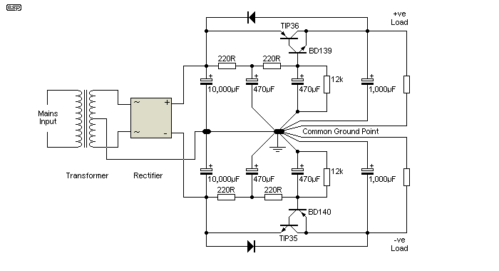
Figure 3A - Complete Dual Capacitance Multiplier (Sziklai Pair)
The voltage drop across the series pass transistor can be reduced if a complementary (aka Sziklai) pair is used rather than the Darlington connection shown. For the positive supply, the driver may be a BD139 (NPN), but the output device would be TIP36 or TIP2955 (PNP). See Figure 4 for an example. This arrangement has almost the same gain as a Darlington pair, but the lower forward voltage may be considered an advantage as overall dissipation is slightly lower.
Note that this circuit is quite suitable for Class-AB amplifiers, but since their current requirements vary so widely, adding a much larger capacitance to the output is a must. The diode is recommended as shown to prevent the possibility of reverse biasing (and destroying) the transistor(s) when power is removed.
The benefits of such filtering are subtle, but may be worth the effort. Many power amps are now built with truly massive capacitance after the rectifier. This reduces hum which is introduced into the signal during loud passages. In theory, this is inaudible - but if so, why do amps with very large capacitor banks always seem to sound better? (Or so the reviewers keep telling us.)
If you are desirous of trying this circuit with a Class-AB amp, I would strongly recommend that the input to output voltage differential be increased (reduce the 12k resistor to do this). For optimum performance (depending on output voltage, the current variation, etc), I would suggest that a differential of 6V to 10V should be Ok, depending upon the power of the amp. Dissipation will need to be calculated (or measured), and remember that Class-AB amps can (and do) create peak currents which can be very high indeed. For the 20V (nominal) supply shown, peak current into an 8 ohm load is 2.5A (which was the design goal in the first place), but if the voltage is increased, peak currents increase in proportion.
As an example, consider a 100W amp (8 ohms). Peak current into a resistive load is about 3.6A, but when driven into a typical speaker load (whose impedance dips to (say) 3 ohms), the peak current will be 9.6A. This is not mere speculation, but reality - such peak currents are quite common - one of the reasons many manufacturers quote the peak output current of their amps. These specs can be as high as 40 Amps or more (for a 100W unit), which is overkill as it will never be used (40A requires a load that falls to 1 ohm - not a speaker I'd ever buy).
It must be remembered that this circuit acts in a manner very similar to a regulator - just without the regulation. If the output current is highly transient in nature, the circuit will allow hum to pass if the input voltage suddenly drops due to increased load (in the same way a regulator will).
Also note that the supply voltage to the power amp(s) will be modulated by the instantaneous current drain of the amp (which happens with 'conventional' supplies too). Maintaining a voltage differential sufficient to accommodate these variations is imperative.
When a capacitance multiplier is suddenly loaded, there may be some ripple 'breakthrough', because the voltage across the circuit is reduced when the load current is increased. If the voltage across the series pass transistor falls, there may not be sufficient reserve for the minimum value of ripple voltage (as described above). It is very uncommon to find capacitance multipliers used with Class-AB amplifiers, because their supply current is constantly changing.
Project 36 (Death of Zen or DoZ) is a simple Class-A amp that can really benefit from using a capacitance multiplier. To reduce the stress on the series pass transistor, it's easy (and probably cheaper) to build two capacitance multipliers as shown in Figure 4. Each multiplier is designed to provide the required single supply of 30-35V DC. By using separate cap multipliers we also isolate each amplifier, so they are very close to being mono-blocks, with only the power transformer being shared.
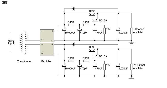
Figure 4 - Complete Dual Capacitance Multiplier (Single Supply, Complementary Pair)
This scheme is similar to that shown in Figure 3A, except that both capacitance multipliers are the same. While the earthing arrangement has not been shown diagrammatically this time, it's just as important to ensure that there is a single 'star' earth point, and care is needed to ensure that no ripple current can be re-injected into the DC via stray earth resistances.
If used with the DoZ amp at higher than normal quiescent currents, you may need to either reduce the 220 ohm resistors to around 150 ohms or increase (or even remove) the 12k resistors to get 30-35V DC from a 30V transformer. Dissipation in the TIP36 (or whatever you decide to use) will be around 6-7W with a current of 1.7A, so there's not a great deal of heat to get rid of in the heatsink.
Expect the output ripple to be around 1mV RMS or less with a current of 1.7A, with ripple being lower at lower output currents. Even with 10,000µF main filter caps as shown, there will be a fairly high ripple voltage on the raw supply, but the output ripple is reduced by more than 50dB when the capacitance multiplier is used.
While it is certainly possible to reduce the ripple even more, it adds much complexity to the circuit and the benefits are doubtful at best. With a power supply rejection of better than 50dB itself, DoZ should be noise free into even the most sensitive of horns when powered by a capacitance multiplier power supply.
A capacitance multiplier doesn't have to use bipolar transistors, but they will usually be the easiest option. The ready availability of good complements (NPN and PNP), low prices and ease of use mean that most people will use this option. However, a MOSFET version may be attractive in some cases, but initial testing (by simulation) indicates that transient performance is very poor - much worse than a circuit using otherwise identical values for passive parts but with bipolar transistors.
If the load current is steady and you can tolerate the higher voltage drop across a MOSFET, then by all means try it for yourself. There are MOSFETs with a low gate threshold voltage (VGS) and this reduces the power dissipation. However, these will almost certainly not be available in complementary versions (N-Channel and P-Channel).
The greatest advantage of using a MOSFET is that the filter section can be higher impedance, meaning that less capacitance is needed for a given hum attenuation. The trade-off will usually be higher dissipation, so a larger heatsink is needed. Heatsinks are bigger and more expensive than capacitors, so there's no economic benefit. Because the gate insulation layer of MOSFETs is sensitive to over-voltage, you also need to use a zener diode between gate and source to prevent damage under fault conditions.
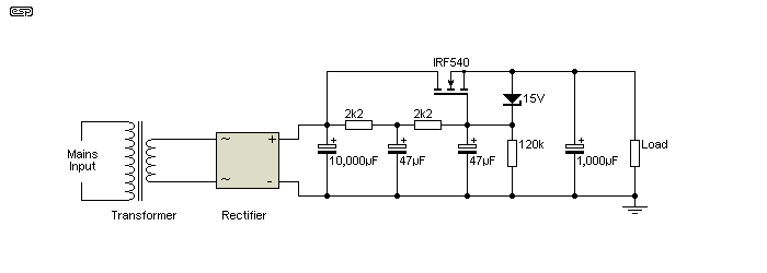
Figure 5 - MOSFET Based Capacitance Multiplier
A sample circuit is shown above. The time constants of the filter network are identical to those shown in the other examples, and hum attenuation is improved by around 10dB - but only if the load current is constant. As noted, the hum breakthrough when transient loads are applied is far worse than a bipolar version (by at least 20dB), and it lasts longer as well (around 500ms for the MOSFET, less than 200ms for the bipolar transistor version). These figures depend on the load current, amount of current change, rate of change (etc.), and should be considered as representative only.
Overall, the MOSFET version is interesting, and it may well be useful for providing a very low noise unregulated supply. However, it performs badly if the load current isn't constant, and it also dissipates more power for a given output current than an equivalent circuit using bipolar transistors. You also need to be aware that vertical MOSFETs (aka HEXFETs) have a limited SOA (safe operating area) when used in linear mode, so care is needed. While it may seem counter-intuitive, MOSFETs with a high RDS on (on resistance) are somewhat safer when used in linear mode. Make sure that you verify that the MOSFET will always remain within the SOA indicated in the datasheet.
 Main Index
Projects Index
Main Index
Projects Index