
|
| Elliott Sound Products | Useless Designs |
 Main Index Articles Index Main Index Articles Index |
There are countless circuit diagrams on-line for almost anything you can imagine. Some are well thought out, well presented and at least look like they should work. However, many are best described as crap - they will either not work at all, or will have very poor performance. Many you'll see are not drawn as schematics, but show pictures of the parts with random wires going all over the place. You'll find this nonsense on search engines, and especially on Facebook - when you see it there it's pure click-bait. Expect to see many comments, most supposedly positive, and most likely fake (added by 'friends' or faked accounts). As click-bait I understand - someone is attempting to direct you to malicious downloads or phishing sites to try to steal your credentials, otherwise I have no idea about the motivation of the useless turds who publish this crap as it serves no useful purpose whatsoever.
For the purposes of this article, I've only looked at audio power amps. I used '150w power amp' as the search term, and got a range from 15W (if you're lucky) up to 1,500W. Some were completely useless, and there are a number of web sites that are best described as 'serial offenders'. Most of the material presented has either been stolen from other sites (such as mine), or is so bloody awful that no one else would want it. The examples shown below were chosen on the basis that they look like they might work for those with little or no experience of circuit analysis.
Needless to say there is an equally ill-conceived 'circuit' for almost any electronic function. These are so common that in many cases they make real (i.e. fully functional and properly drawn) circuits hard to find because they are obscured by crap. It's not only circuits - mechanical contrivances are equally prolific, especially for common functions. There's also the inevitable 'perpetual-motion' machines (aka 'over-unity') often shown powering themselves and an external load. These are (without exception) bollocks, and are commonly faked by various means (AI-generated versions are also probable). It's not known to the average viewer (especially beginners) that they are looking at fakery, as some look plausible. Both the laws of physics and the tax-man agree that you can't get something for nothing - the world doesn't work that way.
I remain puzzled by the rationale of those who present circuits (and/ or videos) that are quite obviously wrong, and/ or are so poorly drawn that it is essential to completely re-draw the circuit before a) seeing that it will never work, or b) realising that the design is seriously flawed. It might work, but with output transistors expected to handle far more than their rated maximum, you know it must fail sooner rather than later. In a great many cases, TO-3 transistors are specified - not a good idea considering the high cost of (and difficulty obtaining) this package as a genuine device. If you find TO-3 transistors that are cheap, they are fakes!
You'll see that many of the circuits shown have a URL or watermark, and I've (quite deliberately) left these in place so you can see exactly where some of the offenders can be found. In most cases, these sites seem to have no purpose other than to gain advertising revenue. Some are potentially malicious, and my anti-virus blocked linked content on quite a few of the sites I looked at.
I made no attempt to clean up the drawings I found, and the only 'edit' was to resize them to a width of 800 pixels. The layout and text are exactly as shown in the original, and it's pretty obvious that some drawings are presented in a way that means mistakes are inevitable.
One thing is common - many sites show a (often long) list of drawings, with the most basic description possible. Details of how the circuit is supposed to function are often missing, or there's a link that (attempts to) send you off to another site, which will often be highly suspect. In more than one instance I saw, there's a lengthy description, but for a completely different circuit that didn't appear to exist on the site.
One of the most common errors (for circuits that might actually work) is a complete lack of understanding of the SOA (safe operating area) of semiconductors. Almost every (potentially workable) circuit shown below will exceed the SOA of the output (and/or driver) transistors, so while that amp might function when everything is at 25°C, as the transistors heat up, they will operate well outside their SOA and will fail. Failure is unlikely to be instant, but it's inevitable when devices are operated at their limits (or beyond) at 25°C and the transistors reach 70°C or more. No heatsinking information is shown, and indeed, for most there is not even a mention of the heatsink!
Beware! Some of the sites hosting schematics (of all kinds) are malicious, and good anti-virus will (or should) block them. Threats include malware downloads (without any action on your part) and phishing exploits. It would be unwise to register on these sites in order to post a comment, but even if you were to do so, you can be sure that it will simply be deleted. These arseholes don't care if you like the content or not - they are just click-bait. Some are designed to try to infect your PC, so browsing without robust anti-virus is a very bad idea.
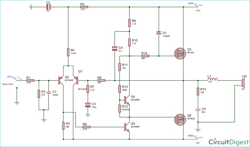
The circuits aren't shown in any particular order. The first is allegedly a 150W amp, described as '150W tone control echo subwoofer active speaker power amplifier'. The drawing is pretty much unintelligible in places, and to get 150W from a 35V supply would mean using a 2Ω speaker. In theory, a 35V supply can provide up to 150W into 4Ω with zero losses and a supply that doesn't collapse under load. Neither is possible in reality.
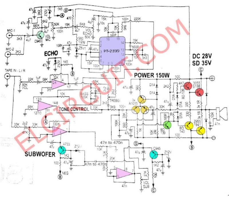
The suggestion to use 3055 and 2955 transistors is fatally flawed, as their peak dissipation into a reactive load will exceed the maximum ratings by a huge margin. The layout is a dog's dinner, and I'm fairly sure that my cat could have done a better job if he put his mind to it.
I've not tried to analyse most of the 'circuit', as there is nothing to be gained from doing so. It's just a mess, and while much of it looks like it will at least function, it's not something that I would ever recommend to anyone for anything. I liked the 'SUBWOFER' (sic) circuit which is rather pointless as the power amp has a -3dB frequency of 48Hz.
Joining the base of the 2955 to the -ve supply is less than inspiring, and that part of the circuit is quite wrong. The base of the 2955 should connect to the emitter of the BD140! The supply is marked as being 28V (DC) or 35V (SD) - WTF is SD? Not stated, so no one knows. The negative supply is not specified.
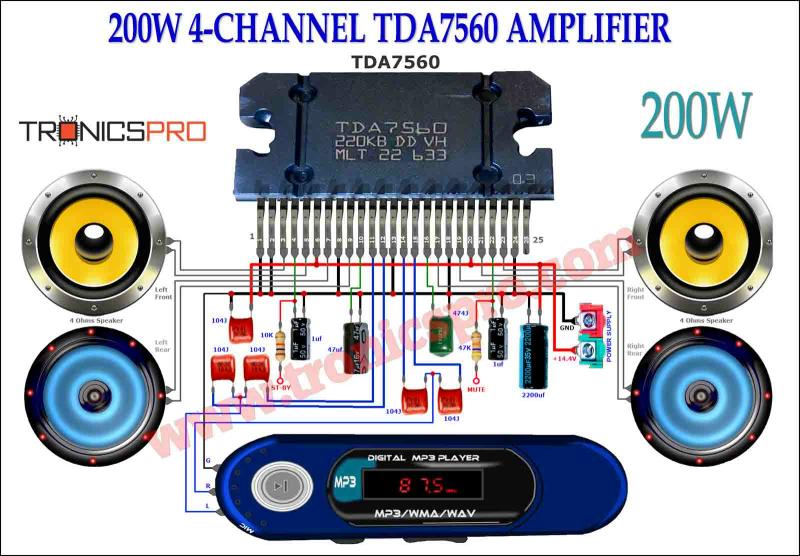
Described as '200W 4 Channel TDA7560 Amplifier Circuit Diagram', the drawing is utterly pointless. The datasheet for the IC doesn't help either, as it claims 4 x 55W into 2Ω (at 10% distortion), and to get that the IC must be clipping heavily. With a nominal 14.4V, the maximum theoretical (zero losses) power is ~52W into 2Ω, but if it manages more than 40W I'd be surprised.
The next circuit is an appalling attempt at a schematic. It fails to follow even the most basic conventions (typically left to right, input to output), and the 'designer' thinks that the complementary TIP142/147 (rated for 125W maximum) will somehow survive with a ±45V supply. Very few speakers will remain above 8Ω across their range, and the transistor peak dissipation can exceed that easily, with no allowance for heatsink temperature rise.
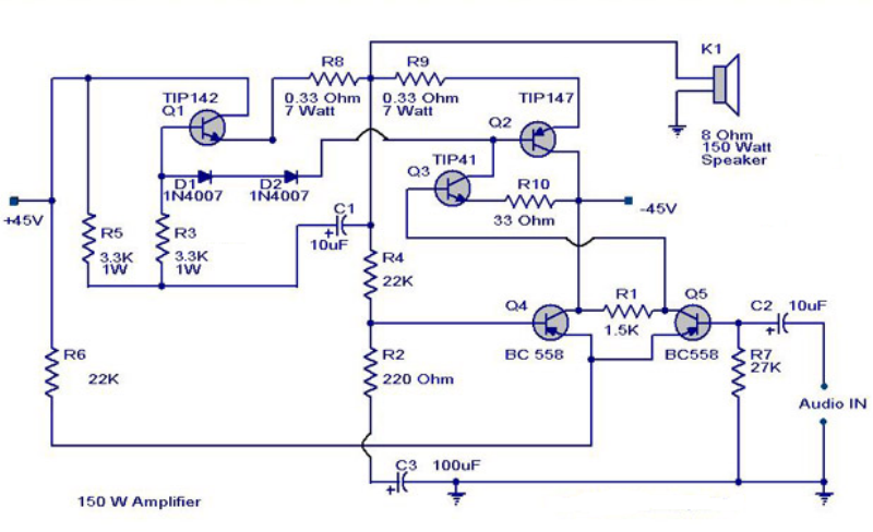
There are only two diodes (1N4007) for bias, so crossover (aka notch) distortion will be high, and will be worse at low output voltages. There's no way it can provide the claimed 150W, because the output transistors plus emitter resistors will drop around 4V, so the effective supply is only ±41V. Should anyone be silly enough to connect a 4Ω speaker the amp won't last long!
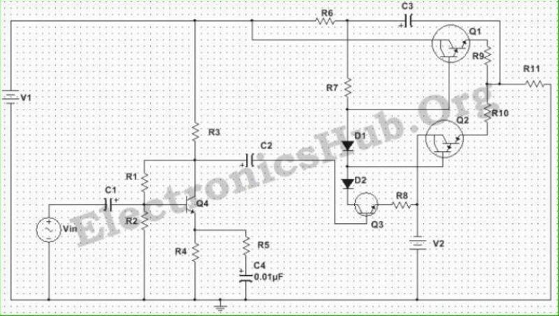
I'm at a complete loss with the next one. It claims to use PNP transistors which is a poor choice as they are rarely as good as NPN types, but (of course) it still uses two NPN devices because it's not possible to use only one polarity for a worthwhile design.

The Class-A driver (2SC1815) has no bootstrapping or active current source, so the positive half-cycles will distort (badly). Of more concern is the feedback, and for AC it has none! The 18k feedback resistor is just shunted to ground at the second transistor, and the idiot who came up with it thinks that a 100nF cap in parallel with the 100uF feedback bypass will help somehow.
There are so many errors and poor design choices that I don't intend to look at them all, but it should be obvious to anyone that expecting 240W from a ±35V supply is not possible with anything more than a 2Ω load. Completely useless!
The next offering goes a step further. Two pissant 2N3055/MJ2955 are rated for a maximum voltage of 70V and 115W. The ±42V supply exceeds the voltage rating. People attempting this would likely use MJE3055/ 2955 types as the originals are obsolete. These are even more limited, with only a 60V and 75W maximum rating.
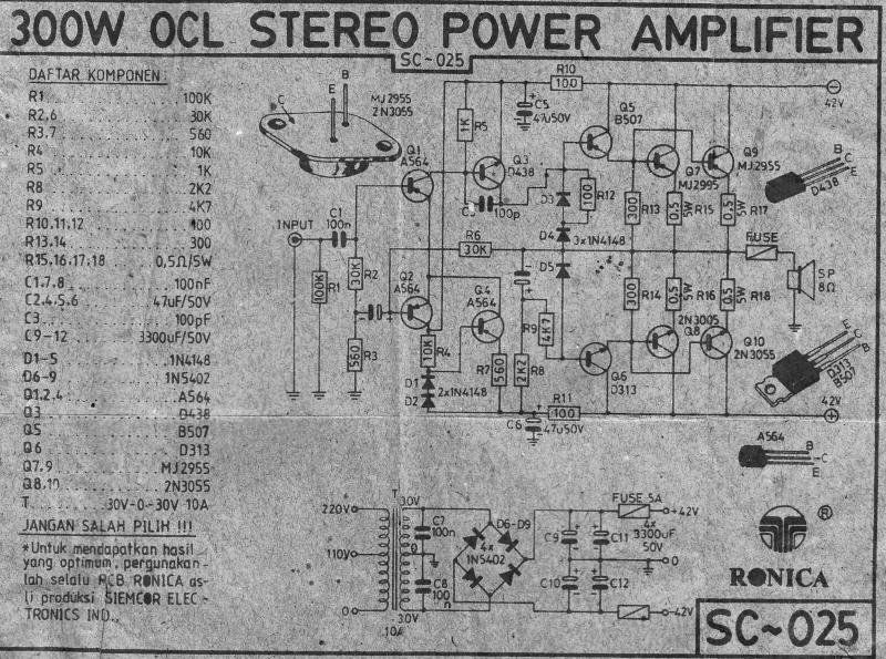
The circuit's been drawn 'upside down', with the -ve supply at the top (against all common conventions). To confuse the issue more, the power supply is shown with +ve at the top. That's really clever! In case you were wondering, 'OCL' means 'output capacitor-less', to differentiate the circuit from single-supply amps that used an output coupling capacitor.
The input long-tailed pair is drawn in a very unconventional and non-intuitive manner, and the input bias resistor (R2) is bootstrapped (a stupid idea for a power amp) Why 30k? 33k would work just as well (or just as badly). A string of 3 diodes is not enough to eliminate crossover distortion, especially when one is bypassed by a resistor. R12 (100Ω) will have about 600mV across it, so the bias current will be close to zero. Neither the feedback bypass cap nor the bootstrap cap are numbered, and they aren't shown in the BoM either.
MOSFET amplifiers are now quite common, but those using switching transistors are always a concern. Lateral MOSFETs were designed for audio, and while they have relatively low gain, they are extremely rugged and reliable in service. The same cannot be said when using small (TO-220 case) devices, as it's not possible to get an acceptable thermal transfer from the die to heatsink. That never concerned the 'creator' of the following circuit though.
Using IRF530/ 9530, the maximum output current is 15A with only 4V across the MOSFET! With 20V across the device, the maximum current is a mere 3A, so it will be outside its SOA (safe operating area) for most of the time. Switching MOSFETs are a poor choice for audio, because they are designed specifically for ... switching!
Word fail me! This is so ill-conceived that I can't even begin to imagine who thought it was a good idea. The Class-A driver (Q3) has no base bias, so the output will swing to the positive supply, forcing DC through the speaker. The way the circuit is drawn is an abomination, as is the whole idea. The watermark shows where it came from, and they should hang their heads in shame.
No component values are shown, but that's the least of the circuit's problems. Circuits like this are of no use to man or beast, and are at best a waste of electrons. The website has a complete description of this design, but completely fails to notice that it cannot possibly work. The site says "This circuit is theoretical and the output contains distortion." It ignores the multiple errors, both in the schematic and the accompanying text, and fails to mention that it will destroy almost any speaker instantly if built as shown.
Another travesty, with a guarantee that there will be considerable DC across the speaker as it uses a single supply and has no output coupling capacitor. Drawing a 'schematic' in this manner is supposedly to 'assist' newcomers to the hobby, but they will be discouraged very quickly if their first attempt at building an amplifier damages or destroys the speaker.

The website shown on the drawing is full of similar circuits, almost all of which are just as bad as the one shown. The author asks you to 'buy me a coffee' - not a chance, as the circuits will do more harm than good to any aspiring electronics enthusiast's career. The maximum output power without distortion (ignoring speaker damage) is around 1W ... if changes are made so it will function. It's actually very close to the circuit shown in Fig. 11, except that the biasing diodes are the right way around, and the Fig. 11 circuit includes a cap to keep DC out of the speaker. Neither circuit will work as shown.
The next one might be able to work, but there would be no point attempting it. It appears to be intended as a drive stage, with external power transistors that aren't included. The supply voltages are limited by the transistors used, so it wouldn't matter much how big the final output transistors are, the maximum power can only be about 60W (8Ω). The gain set by the feedback network is 101 (40dB) - a stupidly high gain, and quite unnecessary for audio. Most power amps have a gain of around 25-30dB, and more is just silly.
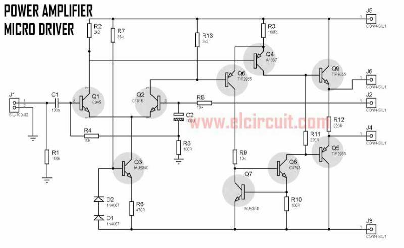
I have no idea what this design is supposed to be for. The term 'power micro amplifier' (or power amplifier micro driver) has no meaning in the world of audio, and it can never work because the two diodes used to bias the current source (Q3) are reversed! Q3 will just turn on (hard), probably blowing up the input transistors. It looks like it's meant to drive external power transistors, but it lacks any sensible bias circuit. R11 (220Ω) should be replaced by a bias servo, but it remains a very poor design (even after the errors are corrected). Again, the input is bootstrapped (R4 joined to R5), which is not sensible (or necessary) for any power amplifier.
There's no provision for a dominant pole compensation capacitor (nor an output Zobel network), so it will almost certainly oscillate. This might be the reason for the insanely high gain, as that makes oscillation less likely because there's less feedback.
Powerful? I think not. With the ±30V supplies shown, even if there were no errors in the circuit (there are plenty!), the maximum possible power would be around 50W into 8Ω. The opamp can't be expected to withstand ±30V supplies, and the real output power would be no more than 30W. The word 'travesty' somewhat understates reality! 'Abortion' is probably closer. Even the volume control is shown completely wrongly. The way it's drawn just makes it so much worse.

Just about everything is wrong with this circuit. The 4558 opamp is powered from ±30V rails via 1k resistors, but with no supply bypass. The second half of the 4558 (used as the input) is meant to have a gain of 3.6, but the output is taken from the inverting input so that won't happen. The output stage is unbiased, so crossover distortion is assured (and in copious amounts).
There are quite a few other errors, but I'll leave it to the reader to spot them. Like the others so far, it's an abomination and the very best one can say about it is that it's a waste of the electrons needed to create it and serve it on the internet.
For another example, and one that's clearly the furthest out of touch with reality, look at the following 'circuit'. I have no idea what 'with trans' is supposed to indicate - presumably 'transistors', but that's already quite obvious. What won't be so obvious to beginners is the multitude of errors, coupled with the insanely over-inflated power rating.
If the circuit were modified so it will function, you'll be hard-pressed to get more than 1W (yes, 1W) into an 8Ω load, and perhaps a fraction more into 4Ω. The circuit is riddled with errors, such as the bias diodes facing the wrong way, the collector of the driver transistor connecting to the junction of the two diodes, and the lower diode connected to the base of the MJ2955 with no path for the base current.
The 100k resistor to the base of the driver can't possibly provide enough current to turn on the transistor (it can provide a nominal 60μA), and the collector load resistor (680Ω) has no bootstrap circuit or other means of supplying adequate base current for the 2N3055. I did simulate this one (just for the fun of it), and it is every bit as bad as I expected it to be.
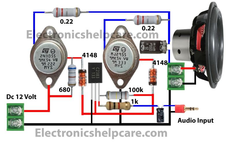
It's worth looking at one which is quite possibly the most extreme example of absolute crap. Again, our 'friends' (and I use that term in the loosest possible sense) have created the following monstrosity. This shouldn't warrant a mention because it's so bad, especially when it's described as following - "The circuit's flexibility and ease of use have contributed to its enduring popularity among audio enthusiasts.". I cannot think of a single person who would have gained any benefit whatsoever, as it doesn't (and can't) even work as shown.
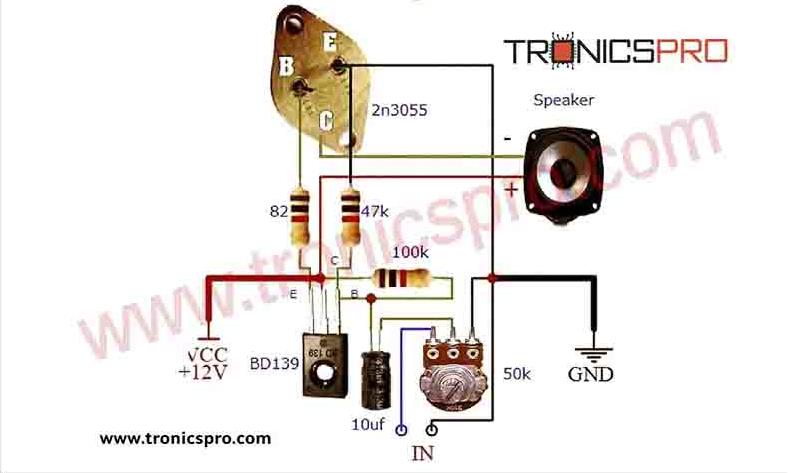
The output transistor's entire collector current flows through the speaker, ensuring high distortion and excessive dissipation in the voicecoil. The transistor will run very hot if you manage to bias the circuit so it will work (as shown, the BD139 transistor doesn't have enough base current to turn on, so distortion would be horrendous). There's also no bias stabilisation, so it might (kind of) work if the transistors are hot. The circuit is a disgrace, and should never have been published.
I have no intention of showing the correct resistor values to bias the circuit, and I consider it a disgraceful act for anyone to publish such a poor design for hapless beginners to construct. Their disappointment (and collection of failed parts) will discourage constructors, who will assume that they made a mistake, rather than blame the cretin who published it.
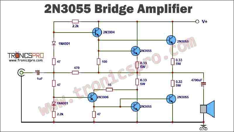
Another from the same site, which absolutely cannot possibly work - at all. Described as a '100W 2N3055 Bridge Amplifier', it's not a bridge amp, and will disappoint even the most pessimistic constructor. Even if it did work, it would be capable of around 8W into 8Ω using a 24V supply (as shown on the website). Just to make things 'interesting', the 2N3906 (PNP) transistor is reversed. Once that error is fixed the circuit is only very marginally less useless. If you think that you need a -3dB low frequency rolloff of 220Hz, a maximum of 5W with over 10% distortion then this is the design for you!
I really don't understand why people publish circuits that cannot possibly work as claimed. It's a waste of everyone's time, and those most likely to be caught are beginners. Until one has a certain amount of experience, it's not possible to look at a circuit and realise instantly that it can't work as claimed. This is a great way to discourage people who are interested in electronics, because they expect that published circuits have been tested - not unreasonably!
To buy the parts and build a circuit only to discover that it doesn't work may prompt some to try to work out why, but beginners don't know enough to know what to change (or why). To give you an idea, it turns out that the Fig 13 circuit is less than unity gain, with a very low input impedance (about 600Ω). It has massive crossover distortion and a maximum output before clipping of about 16V p-p (5.6V RMS). For that, it uses two pairs of output transistors.
The site claims that "One such circuit that has gained immense popularity is the 100W 2N3055 Bridge Amplifier Circuit Diagram. This circuit is widely used in audio amplification applications and offers excellent performance characteristics." (direct quote). Bullshit! The entire write-up is just word-salad, and looks like it was generated using AI. We really need some actual intelligence, rather than relying on artificial stupidity. As someone who has strived to provide useful information for over 25 years, this crap really pisses me off!
In this article, I've looked at audio amplifiers. However, similar nonsense circuits can be found under almost any category of electronics you can think of. Power supplies are a favourite, with so-called 'regulators' that are nothing of the sort, being simply variable supplies with zero regulation and very poor specifications (not that the specs are provided). There aren't many preamps that use the same pitiful drawing style, but there are a few, including tone controls with no amplification (a waste of time).
Not surprisingly, the same websites shown in the above drawings are the source of many of the useless power supplies and preamps you'll find. You will also see 'transformerless' power supplies on some sites. Where these should always include dire warnings about the danger of these circuits, some fail entirely, with one that I saw giving a lengthy description of a circuit that was completely different from the one shown. I've provided a complete write-up of Transformerless Power Supplies, and it's probably the only description I'd recommend. Not because I wrote it, but because it describes the many dangers (many of which are ignored elsewhere) and offers a simple alternative that is far safer.
There are countless other circuits that are just as bad as those I've shown, and a few that are even worse. Several 'Class-A' amplifiers that use the speaker's voicecoil as the transistor's load (as seen in Fig. 12) were found, with some claiming output power that's completely impossible - assuming the speaker doesn't fail at power-on!
Almost all of the designs shown are seriously flawed, and while some can probably made to function, for the most part you'd still end up with something that doesn't work properly. Many of the designs will require at least one capacitor to ensure stability (freedom from oscillation, parasitic or continuous), but they've not been included in several circuits. There are a few that are basically alright, but poor design choices mean that the performance is well below what is possible with a more careful design.
Showing amplifier circuits that use a 12V supply and claiming 500W output is just stupid. The best you'll manage with a single-ended amp is 4.5W into 4Ω, but few of those you'll see (of this ilk) will manage even that. In a similar vein, you can't expect a 2A power supply (of any voltage) to provide 10, 20 or more amps into a speaker. Connecting any of the 'amplifiers' shown here to a 12V battery would be a bad idea, since even a feeble lead-acid battery can supply more than enough current to liberate the magic smoke from most of the circuits. A small switchmode supply is safer, as most are protected against gross overloads. This assumes that the reader is silly enough to build anything described above, which I don't recommend. Even as a learning experience, they are so flawed that you won't gain anything useful.
Unless a circuit drawing has a proper description as to its working principles or is a well-known design published on a well-known website it should be treated with suspicion. Beware of wildly inflated power ratings (rantings?) and many errors that will ensure that the circuit cannot function. Providing fully tested designs has always been a goal for ESP, and (almost without exception) every design shown has been built and tested. There are a few designs that have only been simulated, but everything with a PCB is known to work as described.
Anything you come across in a random search will result in multiple designs similar to those described here, and will often either fail when pushed to the claimed output power, or will never work at all. A few may contain ideas that you can use elsewhere, but they are few and far between. Interestingly, as I was finishing this article, I was alerted to a forum post where someone was complaining about a circuit from one of those shown here (I won't say which one). He even bought a PCB for the design, but it didn't work so he was asking for help. From any of these highly dubious sites, any help will not be forthcoming. If it does, it will almost certainly be as useless as the designs published.
Allegedly 'reputable' websites aren't immune either. One in particular maintains images for published articles for up to 15 minutes after publication (ok, that may be an exaggeration on my part), and while the links remain they all end up as 404 errors (page not found). Some of the contributors are also ... unhelpful. In many cases errors are published (which is inevitable), but rather than acknowledging the error and thanking the person who pointed it out, comments are often ignored or the error is fixed without comment. In a few cases, the error remains, and nothing is done to correct it.
The goal of this article is to demonstrate that much of what you find on-line is not even remotely useful if you are attempting to get started in electronics. Failure of a circuit (or damaged speakers, etc.) is very discouraging for beginners, because they will generally trust a publisher to ensure that the circuits they feature are genuine and will work as expected. Publishing complete crap that can never work is not helpful! I don't understand why people do this - all it can ever do is waste parts and discourage beginners.
There are no references as such, although I have left the logos on drawings that had them (all drawings are un-retouched, other than to make them the same width). Despite the URLs being shown, I don't recommend that you visit the websites, as several contained malicious code or links to malware. Unless you have truly excellent virus protection, the risks are too great. Even with truly excellent anti-virus, if you are warned not to proceed, I suggest that you heed the warnings.
Note that I did not seek approval from the websites that published the crap I've identified, because the material they've published is not credible, and in most cases seems designed to deceive the reader. The goal is often advertising revenue, and these publishers don't care how many people they hoodwink with what is best described as bullshit. I'd classify almost all the circuits shown as 'click-bait', as none is credible and most won't work at all (or will 'function' very poorly). Am I pissed off? You can count on that, because these arseholes are wasting everyone's time (and money if they are naive enough to believe the crap they produce).
| Main Index Articles Index |