

|
| Elliott Sound Products | IC Power Amplifiers |
 Main Index
 Articles Index
Contents
Power amp ICs such as the LM3886 and TDA7293 are popular, and for good reasons. The circuits are easy to assemble, with a minimum of external parts needed to complete an amplifier. Unlike discrete amps (such as P3A), the IC power amps are much simpler. However, there are some notable restrictions on the use of these IC amps, due to their comparatively low maximum dissipation limits. For the basic design (which has a PCB available), see Project 19. I used this to build and test the circuits shown in Figures 3 and 6.
By necessity, the output current is limited because it's simply impossible to get the heat from the power transistor junctions to the heatsink efficiently. While an LM3886 can deliver a claimed 40W into 8 ohms from ±28V supplies, power into 4 ohms is limited to 68W (typical), and using ±35V with a 4 ohm load provides the same output, because the amplifier's internal protection circuitry won't allow more current. The internal current limit is ±11.5A (typical, claimed) but it will usually be lower because the SOA protection will reduce it when the voltage (and/or temperature) is higher than 'normal'.
Peak output current is claimed to be 11.5A, but that's for a maximum duration of 10ms with 20V supplies. Operation at full power with 35V supplies pretty much guarantees that the IC's internal thermal protection will operate, shutting down the amplifier until it cools. The (absolute) maximum IC power dissipation is 125W, and that is a lot of heat to move from the IC die to the heatsink via a relatively small thermal tab. The 'full pack' (fully insulated) package has a greatly reduced thermal rating, because the insulation layer is fairly thick and is a poor heat conductor.
Another issue that users face is the IC's SPiKe™ protection system. The acronym stands for 'Self Peak instantaneous Temperature' (temperature is 'Ke' for Kelvin). This protects the IC, but the artifacts are decidedly unpleasant if the protection is triggered while you are listening to music at a level that's above the trigger point. A waveform drawing (taken from the datasheet) is shown below, and it sounds just as nasty as it looks.
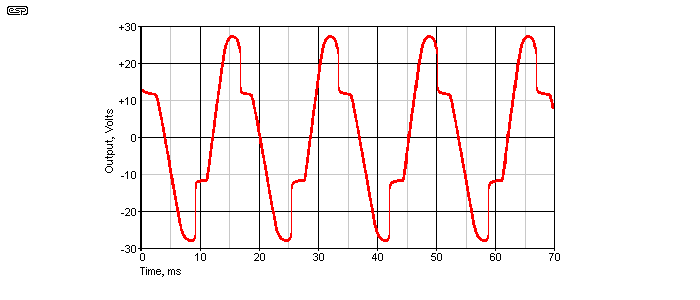
Figure 1 - SPiKe Protection Waveform
The condition under which the waveform was taken are not disclosed in the datasheet, but I know from experience that what you see is typical of the LM3886 driving a reactive load (such as a loudspeaker). It requires surprising little overdrive into a typical 4 ohm speaker, and the only way to avoid the protection circuits from operating with programme material is to reduce the supply voltage. In most cases, ±25V is a sensible maximum for 4 ohm loads, and that (usually) avoids tripping the protection unless the load is especially nasty.
Unfortunately, this reduces output power. While that's often not a problem for home hi-fi used at reasonable levels, the wrath of the SPiKe will come and bite you if you listen at high levels for an extended period. Fan cooling the heatsink (or using a heatsink that's much larger than usually suggested) will reduce the problem, but it won't go away completely.
The TDA7294 has a rated package dissipation of 50W at 70°C. While this seems much lower than the LM3886, the latter doesn't allow for temperature, and assumes a 25°C case temperature. It's a challenge for most hobbyists to work out what they think they can get away with. The allowable power dissipation is reduced as temperature increases, and the maximum die temperature is 150°C, at which temperature the allowable dissipation is zero! The circuit described can also be used with the TDA7294, and all comments apply equally (especially in terms of distortion at higher frequencies).
The TDA7293 has protection, but it's not as drastic as the LM3886, and even if the IC is driven into clipping it doesn't do anything more unpleasant than simply clip the waveform. The challenge with either of these amps comes around if you think of using one to drive a subwoofer. Since you typically need as much power as you can get (within reason of course), neither IC power amp is really suitable.

Note that most of the circuits shown include a 0.7µH inductor in series with the output. This is recommended for the LM3886, but it is entirely optional when boost transistors are added. Its purpose is to ensure that the amp remains stable with capacitive loads, but the load is isolated from the amp IC by means of the 2.7Ω resistor used to turn on the external transistors. It wasn't included in my test amplifier, and no oscillation was seen. If used, the inductor is made by winding 10 turns of 0.4mm-0.5mm wire onto the body of a 10Ω 1W resistor.
Before embarking on any of the ideas shown here, I recommend that you ready the Heatsinks article, as that will help you to decide on how much heatsink you need, and the best ways to mount the IC and power transistors. It's not at all uncommon for hobbyists (and even manufacturers) to underestimate the amount of heatsinking needed for a high power application, and a failure can be expensive - especially if it destroys your speaker(s).
You'll also see that most circuits include a pair of diodes from the output to each supply rail. These are optional, because the external transistors will prevent the IC from going into protection mode, and this is where the diodes are needed (to dissipate back-EMF from the load). Since the protection is disabled, the diodes are largely a 'cosmetic' addition. I didn't use them on the test amp I built, and never saw the IC's protection kick in - even when the amp was delivering over 110W into 4 ohms!
There is a a way to get (a lot) more power from IC amps (actually, several ways). By means of two (or more) external transistors the IC has an easy job, as it only needs to provide the transistors' base current (plus a bit of its own power - it would be silly not to get at least some of the power needed from the IC). This arrangement is far more stable (and considerably simpler) than the versions you'll find elsewhere. These typically power the external transistors from the supply rails (often from an opamp), but the overall concept has some serious flaws and is best avoided. The LM3886 is shown, but the additional transistor arrangement is identical for other power amp ICs. The alternate method is shown in Figure 3, but it's the least 'friendly' of the various techniques.

Figure 2 - Added Power Transistors
By adding a pair of output transistors as shown above, they now handle the majority of the output current. The IC as shown will supply around 1A peak, and the transistors supply 6A (peak) or more, depending on the supply voltage and load impedance. With ±35V supplies and a 4 ohm load, it's possible to get over 100W, with the transistors dissipating an average of 25W (70W peak). The LM3886 will dissipate only around 18W (average) or less than 40W peak. You can even add another pair of transistors (R8 must be increased) to enable the circuit to drive a 2 ohm load.
As shown, we can assume a 'worst case' current gain of around 16 for the transistors (the datasheet claims 10 at 15A, so the estimate is fairly close). That means that when the transistors are passing 6A, the IC only needs to provide less than 400mA to the bases, and a total current of about 1.2A peak. The transistors take most of the stress off the IC, so it should run fairly cool, even when the circuit is delivering over 100W continuous. Naturally, the transistors must be in excellent thermal contact with the heatsink, as their dissipation can be rather high.
This looks like an 'all-win' approach, but as always there are caveats. The main issue you face is distortion. The LM3886 is claimed to have distortion of around 0.03%, but adding the transistors will cause this to increase, with the increase directly proportional to frequency. Below 500Hz or so, the increase is 'acceptable', and may not be noticed. However, at higher frequencies the distortion rises, and you can expect it to reach at least 0.5% at 10kHz. Distortion increases as the level is reduced! It can easily reach over 1% depending on the level, and the only way it can be avoided is with added complexity that provides bias for the output transistors (or as shown in Figure 6, but that's still less than ideal).
This is not 'hi-fi', but the distortion will not be noticed if the amp is used for a woofer (reproducing nothing higher than ~500Hz) or subwoofer, because it is reduced at lower frequencies where the LM3886 has more gain. It's the open loop gain of the IC that ensures that there's enough feedback to overcome the Class-B operation of the added transistors. The circuit is the equivalent of running a normal Class-AB output stage without bias, but the IC provides the power until the voltage across R8 exceeds ±0.7 volts. After that, the external transistors provide the majority of the output current. Another ESP project that uses a similar principle is the Project 68 subwoofer amplifier.
One thing this also does is effectively disable the protection circuits inside the LM3886. If the output is shorted, Either Q1 or Q2 will almost certainly fail, because the IC no longer 'knows' if the current is excessive. There are techniques that you can use that might provide full protection, but it's one of those things that needs to be thoroughly tested if you plan to implement it. Consider that protection circuits are intended to protect the amp against abuse, and many amps don't include protection yet survive for decades without any issues if they are used sensibly. Note that the bypass caps have been simplified for clarity, but they need to be as shown in Figure 2. Additional diodes are shown for these boosted circuits, but they may not be necessary, because ideally the 'SPiKe' protection circuitry will never be invoked.
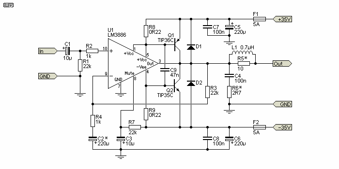
Figure 3 - Added Power Transistors (Alternative)
This version is not particularly common, but I've seen it used and there are a couple of circuits on the Net that show it. There is a potential issue with this arrangement, and that concerns proper bypassing of the power amp IC. You cannot use bypass caps at the IC supply pins, because they will cause cross-conduction in the power transistors, leading to rapid overheating and failure. This is more likely at high frequencies, because the bypass caps slow down the rate of change of the base current into Q1 and Q2.
C9 is optional. There is a small risk that it may cause some cross-conduction if the value is too high, so I suggest that the value shown is a realistic maximum. If the circuit oscillates without C9, it's obviously necessary. This is not an arrangement that I would normally suggest, as it doesn't have any particular advantage over the Figure 2 circuit. Once the current threshold is reached, Q1 or Q2 will turn on just as quickly, and the feedback is unable to provide full correction. The external power transistors will conduct when the LM3886 draws more than 3A from either supply rail, and it's unlikely that U1 will ever have to deliver more than ±3.5A (peak) from either supply rail.
Sometimes, just adding a pair of transistors may not be considered enough, especially for (very) low impedance loads. While such loads aren't usually a particularly good idea (cable losses become excessive for a start), there may be times when you need to drive a low impedance load. The following circuit will drive 2 ohms easily. It may even be possible to drive a 1 ohm load, but I wouldn't advise it because cable resistance will cause too much power loss. It's also difficult to build a power supply that can handle ±25A peak current!
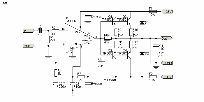
Figure 4 - Added Power Transistors In Parallel
This would normally be completely out of the question, but the extra transistors make it easy to do. Due to the relatively low supply voltage, dissipation remains within tolerable limits, but when run at full power there's still a lot of heat to get rid of. Total average dissipation will be about 125W, with roughly 25W for each transistor and the same for the IC. Total average power into the load should be at least 200W.
Under normal circumstances, it's not really advisable to use most power amp ICs in bridge (aka BTL), because that means the load impedance cannot be less than 8 ohms, and the ICs will struggle with the low impedance. A reduced supply voltage helps, but that reduces power. By adding transistors as shown, the IC can easily drive an 8 ohm subwoofer to around 200W when used in BTL mode. Perhaps more interestingly, if the output transistors are duplicated as shown in Figure 4, you will be able to drive a 4 ohm sub to around 400W, provided your power supply can handle the massive current. Each amplifier has an equivalent load impedance of only 2 ohms.
Mind you, you will have to provide heatsink space for two power amp ICs and eight power transistors. If the suggested transistors are used, it's still a fairly inexpensive way to get 'lots of watts' from a fairly simple circuit. At around AU$3-4 each, they are inexpensive devices compared to those required for a discrete amp. Naturally, higher power transistors can be used in place of the TIP35C/36C suggested, but they may cost more.
You could use MJL3281A (NPN) and MJL1302A (PNP) or similar for roughly the same price as a pair of the TIP transistors, which is a cheaper option because you don't need the 100mΩ emitter resistors. It's very unlikely that you'll ever reach the limits of these higher power devices, as they are rated at 250W each (vs. 125W for the TIP transistors). However, you have less thermal conductivity between the dies and heatsink with the higher power single transistors) and that makes the thermal interface more critical.
Plenty of application notes, DIY circuits and even commercial products have tried using a pair of LM3886 amps in parallel. Pretty much without exception, this is a disaster waiting to happen. I have seen (and bench tested) one commercial attempt, and it was so poorly executed that it was completely unusable. There are several attempts at DIY versions, and some of these also contain serious flaws that are likely to cause ICs to shut down due to overheating ... or blow up.
The issue is that even a very small DC or AC offset causes a heavy current flow between the IC output pins. Most circuits recommend 0.1 ohm, but if there is a 1V difference between the outputs of the two amplifiers, that means a current flow of 5A. A more-or-less representative (but simplified) parallel circuit is shown below. While it may appear to be alright, you must consider the resistor tolerances and IC offset voltages. Note that the drawing is simplified, with the mute taken directly to the -ve supply, and bypass caps are not shown. By using a single capacitor for the feedback coupling (C2), the two amplifiers have exactly the same low frequency rolloff, preventing the likelihood of very low frequencies causing large offsets at the outputs of the power amp ICs. This is missed in most circuits published, but it's an important consideration.
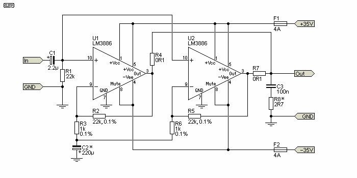
Figure 5 - Parallel LM3886 ICs For More Current (Simplified)
Most circuits use 1% tolerance resistors, and these are usually perfectly alright to ensure that circuits function as expected. However, in the circuit shown you have to check for the worst case error, where resistor tolerances accumulate such as to create the maximum error (as per Murphy's Law). Just for the sake of this example, assume that resistors are exact, except for R2 (1% high, 22,220Ω) and R5 (1% low, 21,780Ω). That means the first IC has a gain of 23.22 and the second has a gain of 23.78. With an instantaneous input of 1V, U1 therefore has an output of 23.22V and U2 has an output of 22.78V, a difference of 440mV.
440mV doesn't sound like very much, but with only 200mΩ between the two outputs, a current of 2.2A will flow between the output of U1 and U2 ... with zero load on the output ! Imagine just how bad this can become if someone is foolish enough to use 5% resistors and the smallest (and separate) capacitors possible the feedback coupling to ground (i.e. separate small caps for each feedback network). I can tell you from personal experience that an Asian manufacturer did exactly that, and the results were completely predictable. This arrangement works only if resistors and capacitors are closely matched (0.1% tolerance ! ), or if you use the (IMO massively over-complicated) method shown in the LM3886 application note.
If 0.1% tolerance resistors are used, you can expect the worst case circulating current between the ICs to be around 220mA at the same peak voltage, which represents a significant reduction. This will reduce instantaneous no-load dissipation from perhaps 28W (in each IC) to less than 3W (output voltage dependent). Note that DC offset hasn't been considered, but this has to be taken into account. It's fairly low of the majority of power amp ICs, but if the ICs are used with full DC coupling it could be as much as 100mV. This approach is obviously unwise with paralleled power amps. You also have to consider the risk if one IC goes into thermal shutdown and the other does not. This was also seen with the unit I've described, and the results were not a pretty sight (at least one LM3886 failed during testing). Worst of all, it's unpredictable because the output stages were never intended to have to sink significant current from outside the IC itself. Especially if the IC is supposed to be shut down!
The best possible advice I can give on parallel operation is "don't !" Yes, there's a Texas Instruments application note (AN-1192) that shows you how to do it, but the requirement for 0.1% resistors makes it more costly than it should be, and even the app note includes an error in the value of the feedback capacitors. They should be at least 100µF, and preferably 220µF to ensure that their wide tolerance doesn't cause serious problems with any infrasonic input signal. Such signals may be thought uncommon, but a warped vinyl disc can easily cause very high levels. If you were to use the parallel-bridged version (shown in the same app note), you then add 4 opamps and even more extra close-tolerance resistors, to end up with a circuit that will cost more than a discrete design. Figure 17 in the same app note is seriously flawed, because the 22µF caps are way too small, and there may be significant circulating current at very low frequencies. Electrolytic capacitors are as far as you can get from being a 'precision' component.
BTL (bridge tied load) is a commonly described application, but with most IC power amps it's not a good idea. The TDA7293 can be used in bridge, but only with an 8 ohm load, and only if the supply voltage doesn't exceed ±35V. Adding external power transistors makes it possible to use LM3886 power amps in bridge, but the overall circuit ends up being fairly costly, and probably isn't an economical option. It's not even a 'simple' circuit, because the PCB layout ends up being quite complex, and the two (or more) power transistors and the IC itself all need to be on the heatsink. Using multiple heatsinks just makes the mounting process harder and more expensive.
Where it's appropriate, it's advisable to use an external balanced line driver circuit to derive the two signals. One signal is not inverted, while the other is inverted. The two signals are in anti-phase, so the effective signal across the speaker is doubled and provides four times the power - in theory. Almost invariably, the combination of low impedance load and high current demand from the power supply means that a pair of 50W amplifiers may only deliver 150W, and not the 200W you expected.
In addition, each amplifier 'sees' half the impedance, so with an 8 ohm speaker, the load on each amplifier is equivalent to 4 ohms. With all IC power amps, this increases their internal dissipation and with sustained high power operation the IC's internal thermal protection circuit may cause one or both to shut down. This can cause a real problem if one shuts down before the other (which is almost a certainty), and the IC that's still operational tries to force current into the output stage of the other. This may cause the IC that has shut down to fail, as they are not designed to sink current. There is no information anywhere to suggest that the common ICs are 'safe' in shutdown mode, and it's normally not a consideration because the IC is shut down.
Along with parallel IC operation, by suggestion is don't attempt bridging with IC power amps unless you test every possibility very carefully before you connect it to your speakers. This is doubly true if you add booster transistors.
Many years ago, Peter Walker (of QUAD, UK fame, 1916-2003) astonished everyone with the 'current dumping' amplifier, the QUAD 405, released in the mid 1970s. It used a low power Class-A amplifier, and added 'dumping' transistors to provide the current when the small amp ran out of power. There were many people (including well qualified engineers) who doubted that it could possibly work, and arguments raged in magazines for many years after it was released. It's doubtful if the arguments have ever actually stopped, and there's a lot of conflicting opinions on the Net to this day. Admittedly, much of the current criticism relates to the noise level (high by modern standards), 'limited' low frequency response (-3dB at ~15Hz) and rather aggressive current limiting, but that's another story.
An iconic article on the subject was written for Wireless World magazine in 1978. Titled 'Current dumping — does it really work?' it was written by J. Vanderkooy and S. P. Lipshitz (University of Waterloo, Ontario). There was much theoretical analysis, but to take measurements they had to modify an audio generator to get below 0.002% THD. The current dumping principle was effectively validated, but the arguments didn't stop. Notwithstanding any of the above, a similar principle can be applied to a boosted IC power amplifier, as shown below.
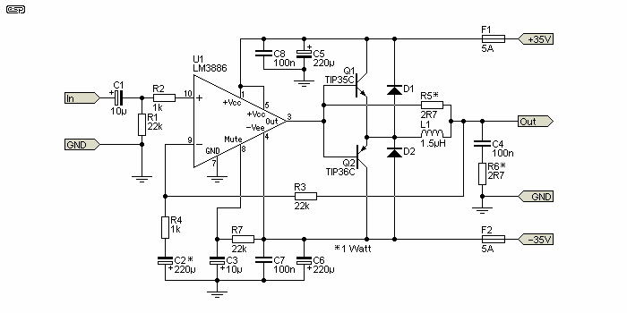
Figure 6 - Current Dumping Booster
Don't expect this to equal the QUAD 405 or any of the later models that used the same technique, but distortion at 10kHz is reduced from around 0.5% to 0.04% (based on a simulation - not a measurement). An order of magnitude distortion reduction is definitely worthwhile. The 1.5µH coil will need around 17 turns of enamelled wire on a 5mm former, wound with a coil height of no more than 12mm. The wire should be at least 1mm diameter to limit power losses due to its resistance. With 1mm wire, the resistance should be just over 0.02Ω. However, see the measurement results described below - in reality there is not much (if any) difference! All the more reason to be wary of simulation results.
It won't make a great deal of difference if the inductance is a little more or less than 1.5µH, because the limiting factor is the IC power amp's open loop bandwidth. Unlike the QUAD 405 (etc.) the open loop gain of an LM3886 at 100kHz is less than 40dB, and there's not enough feedback for it to effectively minimise the crossover distortion of the unbiased output transistors at higher frequencies. I also tried using a 10µH inductor, but that increased the distortion quite dramatically.
While adding the one extra part (the inductor) will take up some space, the reduction of distortion at high frequencies may still be considered worthwhile, and might make the difference between a very ordinary amplifier and one that will satisfy a great many constructors. If you look at the available literature on the topic of current dumping, it's claimed that a bridge using two reactances and two resistors is required, but this isn't necessarily the case. The fundamental part of the process is to 'slow down' the current delivered by the 'current dumping' transistors to the extent that the rate of change is accommodated by the IC's feedback network. By doing so, there are (at least in theory) no rapid transitions that the feedback can't control, and distortion is reduced accordingly.
The distortion in the current waveform from the emitters of Q1 and Q2 is quite high (around 2.5% at 10kHz), but the current through R5 is 'adjusted' via the feedback network to compensate. It's inevitable that the total distortion is dependent on output level (the figures quoted above are at close to full power). As the level is reduced the distortion will increase, but it's not as drastic as you'll measure with the simpler arrangements (without L1). Ideally, the power amp IC should have a much wider bandwidth than is available from any of the available devices, but that's not an option so performance is limited. However, the circuit shown in Figure 6 will outperform all of the others, especially at (slightly) higher frequencies.
I suggest that you don't expect the ultimate fidelity from the circuit shown, but it may be better than the more basic circuits shown above. The only other way to achieve low distortion is to bias the output stage, but this adds a great deal of complexity and doing so makes the final circuit almost as complex as a discrete design, but without the advantages thereof.
The TDA7293 offers an intriguing option, where another TDA7293 IC is used as a 'booster', utilising only the power stage in the second IC. This is described in the datasheet, but the end result is not inexpensive and shouldn't be necessary for the majority of applications. Also described is a Class-G (multiple supply rail) design, with external transistors in a fairly complex arrangement that I doubt any hobbyists have built (and likely no manufacturers either). Since these designs are shown in the datasheet, I don't intend to duplicate them here.
Almost any power amp IC can be used with booster transistors, so for a smaller amp you could use an LM1875 for example, allowing it to deliver more power. The usefulness of this is debatable, since you'd typically only use that device when you only need low power (up to 25W or so), and obtaining more power is limited by the device itself and its supply voltages. There will be an advantage if you wish to drive a 4 ohm load, because the internal current limiting normally only allows the same maximum power into 4 ohms as you get with 8 ohms. With a supply voltage of ±25V (recommended maximum), it should be possible to get close to 40W into a 4 ohm load if booster transistors are added. In terms of cost and difficulty, you'd be better off using an LM3886 (at ±25V or so) instead, as the total cost will be about the same and construction complexity is reduced.
The final alternative is a fully discrete design. The PCB is larger and there are more parts, but the output transistors are usually the only components that need to be mounted on the heatsink. Examples of discrete designs from ESP include P3A, P101 and (for high power subwoofers) P68. These are all well used designs, and generally create very few issues with construction. The numbers built by customers range from many hundreds to several thousand, and these amps are 'mature' designs. There are no surprises, and they all perform exactly as intended.
I built an amp using the techniques shown here, and managed to get over 112W into 4 ohms without any trouble (my variable power supply was the limiting factor, and I had to use a tone-burst to get the measurement). However, the overall distortion is not wonderful, particularly at low levels. From an output voltage (at 1kHz) of around 1.5V RMS up to 4V or so, distortion sat resolutely at a bit over 0.05% which is just alright. At lower levels (where the output transistors don't conduct at all), distortion dropped back to around 0.05%, and it fell below 0.03% at higher levels and approaching clipping. There is no doubt that this method works (and is better than the simple approach), but it's not something I'd suggest for a hi-fi system. If used for a subwoofer, you'll most likely never hear the distortion, as it reduces with reduced frequencies. I didn't run tests at less than 400Hz, but performance was noticeably better just by reducing the frequency by a bit over one octave (from 1kHz to 400Hz).
Somewhat surprisingly, the distortion measured at 400Hz both with and without the inductor shown in Figure 7 was almost identical. A larger inductance was tried (around 12µH) but that made the distortion worse, not better. The maximum distortion measured was 0.04% at 2.4V (RMS) output, falling to below 0.02% at levels below 1.5V. When driving 4 ohms, distortion was roughly twice that measured at 8 ohms, a not entirely unexpected result.
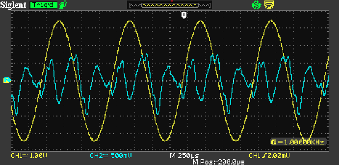
Figure 7 - Output And Distortion Waveforms At 3.4V Peak (2.4V RMS) Output
At any output voltage above around 6V RMS, the distortion fell again, being below 0.03% up to the point of clipping. Unfortunately, this means that the worst case distortion occurs at the levels people are most likely to be listening at, but as already noted, I do not recommend this technique for a full range amplifier.
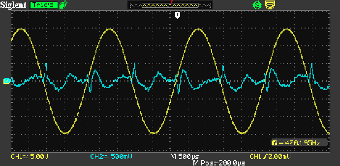
Figure 8 - Output And Distortion Waveforms At 15V Peak (10.6V RMS) Output
The distortion waveform seen has some sharp spikes on the 15V waveform, which are created by the external transistors turning on. While they appear to be at the zero crossing point, they are actually a bit above, and correspond to the turn-on voltage of around 0.7V (peak). Despite the spiky waveform, the distortion measured only 0.02%, and this is a clear indicator of why it's so important to monitor the distortion waveform. Simply relying on the numbers can be very misleading when there are sharp discontinuities in the waveform.
So, the technique works pretty much as expected. I wouldn't bother trying to implement the 'current dumping' version (although it does no harm), and usage should be limited to loudspeaker drivers that have poor high frequency response. When testing, you may not notice the distortion - 0.04% is not particularly wonderful, but it's not exactly woeful either. Beware of very low impedances though, because the distortion rises almost in direct proportion to the impedance reduction. For example, at 400Hz and a 4 ohm load, expect distortion to increase to around 0.08%. I didn't try a 2 ohm load, but I'd expect the distortion to (roughly) double again.
One thing is certain - the SPiKe protection is effectively disabled, and it's possible to get a great deal more power than the IC amp was ever designed to deliver. However, the dissipation in the output transistors can get very high (70W peak, 25W average with a 4 ohm load and ±35V supplies), but also consider that you can get up to 110W output from an IC that's rated for a maximum of 68W (which it normally cannot achieve in real life). Meanwhile, the theoretical increase is just under 3dB, so you have to ask if it's worth the trouble.
In this case, I leave (most of) the conclusions to the reader. Adding booster transistors does allow an IC power amplifier to deliver more power into lower impedance loads than is otherwise possible, but it comes with caveats. The greatest of these is distortion. It won't be audible if the amp is used for a woofer (in a 3-way system) or subwoofer, but is likely to sound rather harsh if you try to use this technique with a full range amplifier. You also have to decide if it's even worthwhile doing - the IC can't be operated at a higher voltage than its rated for, so power into most typical loads won't be improved by much.
Because there's no PCB available designed for boosted operation, there's a degree of messing around needed to get the circuit wired up, but it's not difficult to do. Make sure that power transistors are mounted using thin mica insulators or Kapton tape, and use thermal grease to minimise thermal resistance. Do not use silicone pads - they do not have the thermal conductivity necessary to keep the transistor temperature to the minimum.
I've shown TIP35C (NPN) and TIP36C (PNP) transistors in each of the designs, because they are rugged and very reasonably priced. They don't qualify as 'premium' parts and some may question the wisdom of using comparatively slow devices (FT is 3MHz). In reality, their speed is perfectly acceptable in this role, because they don't need to be fast. At less than AU$3.00 each, this is one of the cheapest high-power transistors available. The 'C' versions are rated for 100V (far more than will ever be used), but the lower voltage 'A' and 'B' versions don't seem to be available any more. 2N3055 and MJ2955 or other TO-3 transistors can also be used, but are harder to mount, more expensive than the TIP transistors.
Once the added complexity of mounting the power amp IC and the extra output transistors onto a heatsink is considered, you need to decide if there's any net gain. Most of the time, a discrete power amp will give better performance anyway, so the wisdom of boosting an IC's output power should be subjected to scrutiny before you start building. Using 'current dumping' is certainly worth trying, and it does give you more insight into things that are possible (whether or not the outcome is 'better'). The cost of the IC power amp (whether LM3886 or TDA7293) has to be considered, and when you add the other parts the cost difference may not be worthwhile.
Warning: Buying IC power amp ICs from on-line 'auction' sellers (i.e. not major suppliers) comes with some risk, as many are not the 'real deal'. Some could be factory rejects, and others may be counterfeits. There is no doubt that some are (claimed to be) genuine, but the sellers are hardly likely to say otherwise.
You need a substantial heatsink (preferably with a fan) if the amp is to be used for any kind of test system. I mention this because I've had a couple of enquiries recently about low frequency current sources, capable of up to 10A RMS into low impedance loads. This kind of arrangement is close to ideal for this kind of application, because it's comparatively straightforward to implement. For sustained high currents (whether AC or DC), using parallel transistors is highly recommended, because it's too difficult to get a low thermal impedance between the transistor and heatsink with a single device. Even using three transistors in parallel isn't as silly as it may sound at first! The power supply becomes critical too, because the extremely high current involved places serious constraints on the power transformer, bridge rectifier and filter caps.
LM3886 Datasheet
TDA7293 Datasheet
Current Dumping Technology (QUAD - 'Our Story')
Current Dumping Power Amplifier - by P. J. Walker (Wireless World, December 1975)
 Main Index
 Articles Index