
|
|
| Elliott Sound Products | Matching Power and Driver Transistors |
 Main Index
Articles Index
Main Index
Articles Index
Matching power transistors is theoretically easy, but in reality there are quite a few parameters that should be matched to get true matched pairs. The situation is made a little harder when you have PNP and NPN (or N-Channel and P-Channel) devices, since the simpler comparison (or bridge) techniques don't work due to the opposite polarities.
This article is not intended to cover all the possibilities, since the equipment needed is out of the range of the average hobbyist. Bear in mind that some of the tests are potentially destructive if the DUT (device under test) does not have an adequate heatsink, so the provision of a fairly substantial heatsink is essential. Ideally, a quick clamping method will be utilised so the devices don't have to be screwed down each time - this can get seriously time consuming.
Manufacturers get around the heatsink problem by pulse testing (so the device does not get a chance to get hot), but this requires expensive equipment to do, so a simpler test is needed. Simpler actually makes it more complicated for high current tests, since you will have to mount the transistor before you start. For these tests, using mica washers is out of the question (too time consuming), so the heatsink will be at the potential of the collector (BJT) or drain (MOSFET).
You will also need a fairly substantial power supply if you want to test at high current. You must also be aware of the safe operating area of the device, since exceeding this will destroy BJTs very quickly. MOSFETs are a little more forgiving, but will still fail if pushed too far. The supply voltage is deliberately quite low (about 12C DC) so that SOA problems should not occur.
An alternative to the method show here is described in Project 177. This is a constant collector current hFE tester for transistors, and because it uses constant collector current, it allows for more accurate matching. It uses a selectable emitter resistor to determine the current, and can provide very accurate results. However, it is more complex than the circuit described here.
WARNING - The rated maximum source to gate voltage of MOSFETs must never be exceeded.
Ideally, you will have two multimeters, but one can be used if you don't have two. The meters will most commonly be digital, and a current range up to at least 2A may be useful (but not essential).
The power supply should ideally be regulated, but if you don't have one, an unregulated supply will still work. Mains voltage variations will affect the accuracy of measurements. Normal variations will not cause large errors, and the final result of 'matched' devices will still have some variations - finding two identical transistors is not normally expected or obtained.
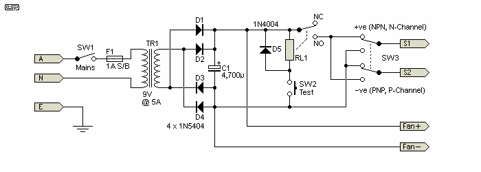
Figure 1 - 12V Unregulated Power Supply
The bridge rectifier needs to be a high current type, and given that 35A bridges are quite cheap, this is a good choice. The 1N5404 types shown are suitable for an output current of no more than around 6A. I suggest that the power transformer should be fairly substantial, or excessive voltage sag will be experienced during testing. A 100VA transformer will be more than sufficient. Feel free to increase the capacitance if it makes you feel better. It won't change anything other than reduced supply ripple, which is of no consequence for this kind of test anyway.

Figure 1A - 12V Regulated Power Supply
Ideally, you'd use the regulated version of the supply. This ensures that the test voltage is stable, and not influenced by mains voltage variations. The regulators need a good heatsink, but since the ground pin (pin 2) is connected to the case, the two regulators can be bolted directly to the heatsink. This improves thermal performance. Thermal compound (aka 'thermal grease') is essential, and the heatsink should ideally be insulated from the case because there is a polarity switch. The internals of the tester should be electrically floating.
RL1 is a relay, typically with a coil resistance of around 270 ohms and with a contact rating of at least 10A at 12V. When SW2 ('Test') is pressed, the relay activates and applies power to the test circuit and the DUT. D5 is used to suppress the relay coil's back-EMF when the button is released.
The heatsink should be designed so that transistors can be mounted and unmounted easily and quickly, or the task will become a chore very quickly. A strong spring clamp will normally be sufficient to keep the transistor clamped to the heatsink and nice and cool during the test, which should still be done reasonably quickly so that device heating does not skew the results. In all cases, the test duration should be kept the same for each device, and a fan is useful on the heatsink to ensure that heating over time does not cause errors (these can become significant with even a small increase of heatsink temperature). The fan can be powered from the supply shown.
The test itself is fairly simple. The first qualifier is for gain, and the emitter-base voltage for BJTs at a known current, or the source-gate voltage for MOSFETs, again for a known current. This first test should be done with the current set for the quiescent current (per device). Figure 1 shows the set-up, and it is deliberately fairly simple. This will work for BJTs and MOSFETs, without any changes. Remember that when testing MOSFETs, the gate is static sensitive, so appropriate precautions must be taken so the DUT is not damaged. Never exceed the rated source-gate voltage - ever!
You will need some high power resistors. The actual power rating depends on the supply voltage and the test current. For the suggested 12V supply, a maximum test current of 2A is reasonable, so the resistors should be set up as shown below - four 1 Ohm 5W resistors will be more than acceptable for the high current tests. The others should be as described and will give four test ranges to cover most test needs.
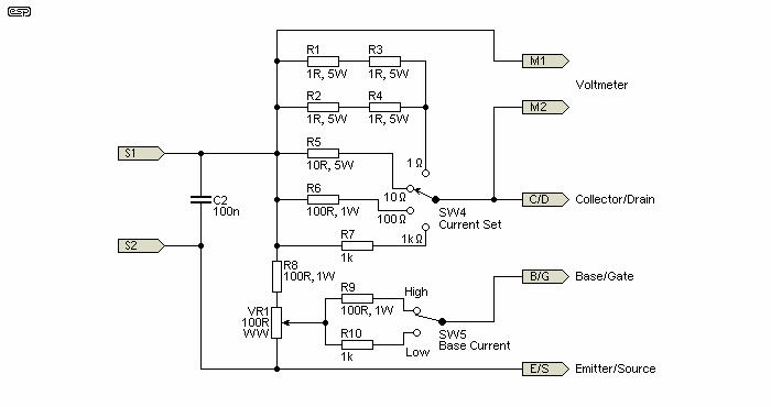
Figure 2 - Quiescent Current Gain / Voltage Test
VR1 needs to be a wirewound pot for testing BJTs, but can be a higher value carbon pot if you only want to test MOSFETs. I suggest the wirewound pot as a matter of course, since it increases the usefulness of the test jig. The pot will get quite warm in operation (it dissipates nearly 1W), so make sure you switch off the power between tests. Test leads should be fitted with colour coded alligator clips for emitter/source, base/gate and collector/drain (BJTs and MOSFETs respectively).
The 'Test' switch (SW2 in Figure 1) is a momentary push-button, and allows you to set up a test without turning off the power. DC to the test circuit and DUT is only present as long as SW2 is depressed, so you are less likely to damage anything when there is no voltage present as you change from one test transistor to the next.
Select a transistor at random from those on hand, and connect it into the test jig. Make sure that the pot is set to minimum, and that the correct polarity is selected first! Set the switch to the 10 Ohm range, press the 'Test' button and adjust the pot until the voltage across the M1 and M2 terminals is equal to 10 x Iq (in Amperes). If you want to use a quiescent current of 100mA, the voltage across the resistor will be 10 x 0.1 = 1V. Remember to divide the total quiescent current by the number of parallel output devices first.
For power transistors, the 'Base Current Range' switch (SW5) needs to be set to the high range (100 Ohms), and base current is limited to about 60mA. With a device having a gain of 20, collector current will be about 1.2A, but that will increase to 3A if the gain is 50 (more common with modern devices). For low power devices and MOSFETs, leave the switch in the low range (~6mA). Note that the maximum gate voltage is deliberately limited to about 6V.
Now you can measure the emitter-base or source-gate voltage. Press the 'Test' button, note the readings, and mark the transistor just tested (so you can correlate the device with its measured characteristics). Repeat the test with the other devices you have, reversing the polarity (SW3) if required - but do not adjust the pot - leave it exactly where it was for the first transistor. Bear in mind that the current in subsequent transistors could vary by several hundred percent, so it may be necessary to readjust the pot and re-run the tests from the beginning.

| It's very important that the transistors being tested are all at the same temperature. This can be monitored with a thermistor and an ohm meter so that the tests are comparable. If you don't manage the temperature properly, the results will not be useful. BJTs change their Vbe (base-emitter voltage) and hFE with temperature, and a higher temperature means a lower Vbe and higher hFE. MOSFETs change their Vgs (gate to source voltage), RDS-on ('on' resistance) and transconductance with temperature. |
For each device, note the emitter-base (or source-gate) voltage, voltage across the resistors (or the current through them), and the reference number you marked on each device. When you have finished, you will have an array of voltages and currents (calculated from the resistor voltage if you don't use a current meter), and you can choose those devices that are the closest match. Generally, only the current is really significant except for devices in parallel, where the base-emitter voltage becomes important. The source-gate voltage will not change if you are testing MOSFETs, so that only needs to be measured once.
By using a higher resistance, smaller devices can be tested in the same way. For driver transistors, the 100 ohm range would be satisfactory, and for small signal transistors, use the 1k ohm range. Be very careful that you keep the current and voltage within the device ratings! The rotary switch on the supply is designed for just this purpose.
Range Measurement Scale 1 Ohm 1A / Volt 10 Ohms 100mA / Volt 100 Ohms 10mA / Volt 1k Ohms 1mA / Volt
When you connect your voltmeter to the terminals, you'll measure a voltage drop across the selected resistance. The table above shows each range and its scale. For example, if you are using the 1 ohm range and you adjust the pot to give a voltage of 2V, the current through the DUT is 2 amps. Likewise, if you use the 100 ohm range and measure 3V, the device current is 30mA. The same principle applies for all other ranges. Keep the maximum voltage below 6V on all ranges (2V for the 1 ohm range) or there won't be enough voltage on the collector/ drain of the DUT.
The test will match devices so that they are approximately equal at the all-important crossover region - if desired, you can test at an even lower current, to ensure that there is the least possible error between devices, however the tests become very time consuming, and obtaining devices that are fully matched over the full operating range is somewhat unlikely.
Once you have a selection of transistors that have approximately equal low current characteristics, you can do a high current test if you want to - this uses the 1 ohm range on the rotary switch. I don't recommend that you exceed 2A, unless you are sure of what you are doing and/or use a higher rated power supply.
The test is set up in exactly the same way as before, except the current is increased to the desired test value. For each device tested, make sure that the test duration is maintained for the same time - say 10 seconds. You will need to wait for the heatsink to cool to the same starting temperature (or near enough to it) between tests. A fan will help here, and is mandatory if you intend to test a reasonable number of devices. Make sure that you allow enough time for the heatsink to return to a known temperature. You can include a thermistor if you wish, which will let you monitor the heatsink's temperature with an ohm meter. The exact temperature reading isn't important, only that you ensure the heatsink is at the same temperature for each test.
Again, you will note the exact current of each device with the pot in the same position as for the first transistor tested. At the end, you will have a set of figures that show the closest matching devices out of those available. I strongly suggest that you don't expect miracles - if you can get transistors that measure within 10% of each other for both the high and low current tests this is a good result. You may do better, but don't count on it, and don't get all depressed if you have to accept a wider tolerance.
For the brave (and those who have taken the time to create a really solid heatsink test set), you can run further tests at higher currents, but you will need to be extremely careful. Remember that 2A at 12V is 24W continuous dissipation, and this will heat the transistor under test very quickly - higher currents will create even more heat.
With the 1 ohm resistor, transistor dissipation is reduced only slightly, and even 24W is a lot to get rid of in any test environment. You will have to use thermal compound for the DUT to prevent overheating, since it will not normally be possible to take a reading quickly enough unless you have access to a digital storage oscilloscope. If you have access to one, pulse tests are recommended for all high current testing. The way to go about this is beyond the scope of this little article though.
An alternative approach is to take your measurements at high and low currents, and then calculate (or plot) the transfer characteristics of each device. Although time consuming, this should give good results. Ideally, you will take measurements at a minimum of three points. Measure collector/drain voltage (and for MOSFETs, the source to gate voltage) at ...
Once you have these figures, you can then select those that represent the closest possible match. You will be very fortunate indeed if you get exact matching, but it should be possible to get several acceptably matched pairs from a batch of reasonable size. You will probably need a minimum of 10 devices, if possible from the same manufacturing batch.
When power transistors are used in parallel, some amplifier designs rely on close matching of all devices. Using an emitter resistor for each device forces some degree of current sharing, but with very low values (less than 0.1 Ohm) the devices should be matched because the resistance is barely sufficient to ensure equal sharing under normal operation.
Matching paralleled transistors usually requires that Vbe and gain are both matched. Gain matching should be done at a range of collector currents to ensure that the transistors share the load equally. It is the nature of bipolar transistors that the one that takes the most load (because of higher gain or lower Vbe) will get hotter, and this will increase gain and lower Vbe even further, causing it to take even more of the load. Use of a common heatsink ensures that die temperatures are held reasonably close to each other.
Using emitter resistors will always help, but in some cases may not be enough to ensure long term reliability - especially if the devices are used close to their maximum ratings. Some designers include series resistors in the base circuits - these might help, but may do more harm than good, and are not generally recommended. With MOSFETs, gate resistors are always needed to prevent parasitic oscillation, but these do not affect current sharing.
Because the temperature of all paralleled transistors should be the same (for the reasons described above), it is essential that all power transistors (bipolar or MOSFET) share the same physical heatsink. By doing this, the average temperature will be very close to the same for all devices. Always use current sharing emitter or source resistors if possible, and feel free to match the Vbe and gain of paralleled transistors (or Vgs and gain for MOSFETs).
The tests described are not the most accurate known, but will be well within the abilities of hobbyists. The results can be expected to be very good when used for matching, and the selected pairs will be much closer than random selection will ever give you.
Matched transistors will rarely give you 'better sound' (whatever that is supposed to mean). In general, distortion will be almost completely unaffected, and there is no influence on frequency response or transient response. What you will get (for paralleled devices) is greater reliability, because the transistors will share the current more equally.
Be aware that some 'low feedback' designs absolutely require that the NPN and PNP transistors be matched, because there is insufficient feedback to make the circuit linear unless the individual devices have closely matched gain across the operating current range. Vbe matching between NPN and PNP devices is not useful with any sensible amplifier design.
The test set is fairly cheap to make, and can be used for all sorts of transistor testing - not only for matching, but to test that transistors are functional. Since it will work with bipolar transistors and MOSFETs, it has enhanced usefulness over most conventional transistor testers for the majority of basic testing needs. The little extras added just make it that much more useful.
Main Index
Articles Index