

|
| Elliott Sound Products | Project 249 |
Guitar 'booster' preamps have been through a number of cycles, starting from non-existent, through to popular, then back to "nah!" (or is that "meh" now?) before interest picks up again. Circuits abound, with the best possible performance coming from well chosen opamps. BJTs (bipolar junction transistors) and JFET circuits are commonplace, but not all are well thought out. Some may place excessive loading on the guitar pickup and circuitry, so output level and frequency response are compromised prior to the signal being boosted again.
Most guitar amps have a nominal 1MΩ input impedance, but that can be as low as 68k when two jack sockets are used for 'Hi' and Lo' gain (although the front panel isn't always clear if it refers to gain or pickup output). With some amps, 'Lo' or 'Low' refers to the gain, and on some others it refers to guitar output level (suitable for low output pickups). I expect that most guitarists have figured out which input they find most suitable, and they'll stay with that. Early amps are probably the least reliable in this respect, as there were no 'standards' (there still aren't, but common usage prevails).
Boosters are used either to provide a simple way to overdrive the amp (with a foot switch), or because the player prefers the sound with some degree of boost and/ or tonal correction applied all the time. There's nearly always a need to be able to preset the amount of boost, which may be as low as 6dB (×2) or as high as 20dB (×10). Booster amplifiers can have a tone control or a fixed treble boost (usually selectable), using either a pot or switched settings. The circuits described are true boosters - they are not 'fuzz boxes', and they are intended only to boost the output from the guitar, with optional basic EQ that can help to get that last bit of bass or treble that may otherwise be elusive.
This is actually a collection of ideas, rather than a single project, so the reader can make a choice as to which technique s/he prefers. There's no reason that circuits can't be combined if you feel that you like one front-end, but prefer to add treble boost or tone controls to a boost circuit that is not blessed with same. Not all circuits can include a treble boost function properly. For example, a JFET booster cannot provide much treble boost when operating at high gain, because there's little additional gain abailable.
Because guitar pedals are expected to run from a 9V battery, the opamp used has to be rated for operation with less than ±4V, and this may rule out the TL07x series. While some will operate from a low voltage, others may not (it's not a guaranteed parameter). The TL06x range ('low power') is rated for a supply as low as ±2.5V and is a safer option, but they are not available from some suppliers. The RC/MC4558 has been a mainstay for guitar amps and pedals for a very long time, and while it's not the quietest opamp around, it is less noisy than most FET input opamps (especially the TL06x and TL07x). However, it uses a BJT input, so noise levels may be greater with a high impedance source. Most importantly, it will run happily with a 5V (±2.5V) supply, and it's an opamp that has a very long history in guitar amps and pedals. They are cheap, and no-one will ever claim they're wonderful, but they have been a staple for guitar effects and amplifiers for a very long time. At less than AU$1.00 each, they won't break the bank, and they only draw about 2.3mA (typical) for a dual opamp.
Another opamp that I recommend is the OPA2134, which works down to 5V. It's a 'premium' low-noise part though, and is not inexpensive. With any JFET input opamp, protection diodes are essential to prevent damage to the input devices from static discharge. Use 1N4148 or similar. Note that they will not provide protection against high current input faults (such as plugging the input into the speaker jack of an amplifier).
If you use an opamp circuit, make sure that it can operate down to 5V or so, or it will stop working as the battery discharges, but before it's reached 'end-of-life'. The LM4562 will work with a total supply of 5V, but they draw a current of up to 12mA, so battery life won't be much good. The OPA1642 is probably the pick of the bunch - under 5mA current for the dual, and operation down to 4.5V. However, they are only available in an SMD package.
Note: It's expected that readers will use the circuits shown as the basis for experimentation. PCBs will not be made available, because there are too many options that aren't directly interchangeable. Most are easily constructed using Veroboard, which is ideal for playing around with ideas. The gain pots will typically be linear, because antilog (aka reverse log) are too hard to get.
This is always a can of worms, because the output level of any electric guitar is dependent on so many factors. Light vs. heavy strings, gentle finger playing vs. a really thick pick (think Dick Dale!), bridge vs. neck (or middle) pickup, the type(s) of pickup (single coil or humbucker), the magnet strength, etc., etc. There is no easy answer, but I did run some measurements on my guitars to get a few basic (and hopefully representative) numbers.
The full details are shown in the Guitar & Bass Pickup Output Voltages article. On average (taken with a variety of guitars and pickups), you can expect a level of between 25 and 80mV RMS, with peaks between 150 and 600mV. The peaks (just as the string is released by a finger or pick) are typically between 15 and 20dB greater than the averaged RMS voltage, and the level tapers off at a rate determined by the guitar itself. Some have more sustain than others, so notes/ chords last longer before disappearing into the noise.
In the circuit descriptions that follow, you'll see references to signal clipping (a form of distortion). This simply means that the output signal is too high, and it can't exceed the supply voltage. When that happens, the signal is 'clipped' at the maximum peak voltage it can reach in a given circuit. An opamp can drive low impedances easily, but it's harder with discrete transistor (including JFETs and MOSFETs). These use a load resistor, and its value determines how much current can be supplied to the following stage. When loaded, most transistor (including FETs) circuits will clip asymmetrically, because the transistor can supply more current than the load resistor. Most guitar amplifier input stages will start distorting well before the output of the booster starts to clip.
It's important to understand that the output impedance of any circuit does not mean it can drive that impedance. Opamps can have an output impedance of well below 1Ω, but they cannot drive impedances much below 1k or so (opamp dependent) at any significant voltage level. This is an area where many beginners (but not only beginners!) can get seriously confused. However, it's not hard to grasp once you understand the concepts.
There are four choices here, being an opamp, a dual transistor stage, a JFET and a small-signal MOSFET. The two options for the tone control section (if used) are shown further below. The opamp is by far the most predictable and linear, and it has the lowest output impedance. This is important if you include tone controls, but the output can be taken directly from the booster amp if preferred (the output resistor and optional output socket are shown for each variant). The circuits don't include a bypass function, but that's easily done with a foot-switch. The drawing showing 'true bypass' is shown in Figure 8. Many people like the idea that the pedal is completely out of circuit in bypass mode, and it means that the signal can still get through if the battery or power supply fails partway through a set.
In the following drawings, the option to use only the booster is shown, with the output resistor shown as R9 in all circuits. This is purely for consistency, and reflects the values shown for the opamp tone controls, which provides the best performance. If you use the opamp controls with a transistor, JFET or MOSFET booster, the other half of the opamp (assuming the use of a dual device) is not used. Whenever an opamp isn't used in a circuit, the output and inverting input should be joined, and the non-inverting input returned to a DC voltage of ½ the supply voltage.

Figure 1 - Opamp Booster Stage
The maximum gain is set by VR1, and is about ×8.6 (18dB). The gain can be varied from unity to the maximum, and if you think you need more gain, decrease the value of R4. For example, if R4 is 560Ω the maximum gain is increased to about ×15 (23dB). While you can easily get more, it's unlikely to be useful. Another big advantage of the opamp booster is that it can drive a tone control circuit easily, without significant distortion (unless the gain is too high and the tone control circuit causes clipping. The ½ supply voltage (Vref) is created in the power supply circuit (Fig. 7) and is shared with the other half of a dual opamp, as used for a tone control circuit as shown in Fig. 5.
The optional 'BP Out' (bypass output) provides a unity gain output regardless of the pot setting. DC is removed by C2, and the output impedance is less than 1k. If used, this lets you use a SPDT (single-pole, double-throw) switch for bypass, and it makes a very good line driver. Unlike the 'true bypass' system shown in Figure 9, the one shown here won't work without power. If this is important to you, then use the Figure 9 circuit. The current drawn depends completely on the opamp you use. A 4558 will draw about 2.5mA.
Using transistors means more parts overall, and the input is also subject to power supply noise (mainly via R1, but everything connected to the supply rail can inject noise). Power supply rejection is only 32dB with the input open-circuit. The circuit shown used to be common in the days before opamps, and it performs reasonably well. The two transistors are in a feedback loop (AC and DC) formed by R5. VR1 changes the amount of AC feedback without changing the DC conditions (hence the inclusion of C2 in series with VR1). With 'sensible' gain settings, the circuit will still operate well down to about 7.5V (a dead-flat 9V battery), but if run at maximum gain you may get some clipping with 'hot' guitar pickups. The following circuit will draw around 2mA with a 9V supply.
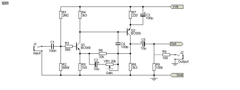
Figure 2 - Dual Transistor Booster Stage
The input impedance is lower than the opamp version, at a bit over 500k. This will rarely cause any issues but some players may prefer that the input impedance be higher than that. The gain is a little lower than the opamp version. It can be varied from unity to a maximum of 8.6 (18.7dB). It's unlikely that you'll need more, but if you do, the opamp is a better choice. The circuit shown is based on the circuit shown in Figure 3b in the article Opamp Alternatives, with changes made to allow operation from a 9V supply. Any of the other circuits shown in the article can also be used, but values will need to be altered to bias the circuits from 9V, rather than the +18V supply used for most of the examples.
The output impedance of the Figure 2 circuit is about 350Ω with maximum gain (it's reduced as gain is reduced). While 350Ω is higher than desirable, it can drive the tone control circuits reasonably well. Most basic transistor circuits will be similar, as it's not possible to get exceptionally low output impedance without an opamp (or a much more complex circuit than the one shown). The current drawn will be about 1.7mA.
Of course, the circuits shown thus far are not the only way you can build a booster. JFETs can be a good choice for reduced noise, but they will almost always need either an adjustment trimpot or hand-selection because the characteristics are so variable. The parameter spread of JFETs is well known, and there nearly always has to be a method of adjusting the bias, especially for low voltage operation. MOSFETs can also be used, but small signal types such as the 2N7000 also have a significant parameter spread, and a means of adjustment is required for them too. Unlike (decent) JFETs, MOSFETs are usually pretty noisy (and this was verified with a bench test). Depending on your playing style and general preferences, this is either a problem or not. If you use a MOSFET, some form of gate protection is essential. If the maximum gate-source voltage is exceeded (even momentarily), the MOSFET will fail.
In order to get a low output impedance, an emitter follower is included on the JFET booster circuit. You could use another JFET as a source follower, but it may need separate biasing for use with a 9V supply. A BJT is far more predictable, and they have a higher gain than JFETs. This minimises loading on the drain resistor and prevents a loss of gain. This is particularly important if the booster is expected to drive tone controls. JFETs have limited transconductance (which affects gain), and expecting more than ×20 (26dB) is probably unrealistic. However, this is usually plenty for a booster.

Figure 3 - JFET Booster Stage
TP1 is a trimpot, and it should be adjusted to get about 3.9V at the emitter of Q2. Depending on the JFET you use, you may need to increase or decrease the value of R3 to enable the operating conditions to be set correctly. I've shown a 2N5484/5, but you'll almost certainly have to use what you can get. They have a mutual conductance (or transconductance) of between 2mmohs and 7.5mmhos (2-7.5mS [Siemens]), which is quite a bit more than a 12AX7 valve (1.25mS with 100V on the plate), included for comparative purposes only. The current drawn will be around 3.1mA.
For detailed information on JFETs, please refer to the Designing With JFETs article. These devices are always 'difficult', because of parameter spread. The range of suitable JFETs has also shrunk alarmingly over the past few years, and once common devices are now difficult or impossible to obtain from major suppliers.
The emitter follower is included to ensure a low output impedance, but for a booster only (no tone controls) the output (to C5 etc.) can be taken directly from the drain of the JFET. The disadvantage is that the output impedance is fairly high. With a 3.3k drain resistor, output impedance is 3.3k, which is still low enough to drive a cable with no HF loss. The minimum gain available depends on the setting of TP1, and will around 6dB with a 'typical' J113 FET (although that's potentially misleading because the parameters are so variable).
JFET boosters will generally fall into one of two 'camps'. Some players love the asymmetrical distortion which adds even harmonics (2nd, 4th, etc.) while others hate it. It's also possible that some players are ambivalent, but that's an uncommon sentiment is the world of guitarists. 
The MOSFET approach has a significant disadvantage, especially if you need lots of gain. The gate-source capacitance (CISS) causes the input impedance to fall at high frequencies. This 'feature' isn't shared by JFETs (well, it is, but to a much lesser degree). However, a MOSFET such as the 2N7000 has much higher transconductance (320mS) than a JFET, and can provide far more gain. I was going to include a circuit but decided against it, as my tests showed that the 2N7000 (and its ilk) are just too noisy.
A MOSFET throws up a couple of other complications. To try to get a passably stable positive gate voltage, it's best to allow some feedback from the drain. However, by itself that would apply negative feedback for AC as well as DC, so it needs to be decoupled. To account for parameter spread, a trimpot is required. While the DC feedback does help to stabilise the operating voltages, the parameter spread is such that the feedback alone isn't enough. It would be sufficient with a higher supply voltage, but 9V is rater limiting. There's no real point showing a circuit that is generally unsatisfactory, so I haven't  .
.
All things considered, I don't recommend using a MOSFET. I have tested what I thought was a suitable candidate, and while it works (both on the workbench and in the simulator), it is noisy. You also have to include an input capacitor, as the gate is positive and a direct connection to a guitar will remove most of the bias and it won't work. The MOSFET's gate is very susceptible to damage, so protective diodes are needed (another nuisance). Input impedance is alright, but it falls quite quickly with frequency.
As noted in the intro, there are several sub-circuits that can be used. One that I would not normally suggest for guitar is a Baxandall circuit. It can be used with a booster because it is an adjunct to the main tone controls, whereas they are generally not favoured for amplifier tone controls. I don't recall ever seeing Baxandall feedback tone controls used in any amplifier that anyone actually liked (unless combined with parametric EQ to obtain the nuances that most players expect from a 'tone stack'). As an add-on effect, the feedback tone control is predictable and works well.
The circuits shown both rely on the output capacitor on the booster amplifier to isolate the tone control networks from DC. If you use a different booster, the output capacitor needs to be at least 10µF to ensure proper operation. Many 'stand-alone' boosters have a relatively small output cap, as they are designed to be used with an amplifier with high impedance input(s). A smaller coupling capacitor will compromise the operation of the tone controls.
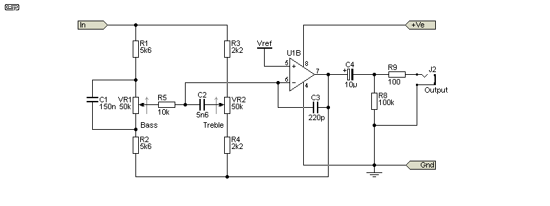
Figure 4 - Opamp Tone Control Module
The input signal must be a low impedance, ideally no more than 100Ω. However, a source impedance of up to 1kΩ can be tolerated, but there will be a loss of around 4dB with the controls centred, and the response becomes slightly asymmetrical. The circuits described will mostly have an output impedance of less than 100Ω, so if you mix and match there should be no issues. It should be obvious, but the tone control (if used) will always be the last circuit in the pedal. U1B will typically be the second opamp in the package, with U1A used for the booster
The circuit is completely conventional, except that the pots are 50k instead of the more common 100k. They must be linear - log pots don't work in this configuration. The capacitor values are selected to give a mid-frequency of around 400Hz, which suits guitar well. The bass control provides ±15dB at 30Hz, and treble gives ±16dB at 5kHz. The turnover frequencies are easily changed by changing C1 (bass) and/ or C2 (treble). Note that Vref is obtained from the power circuit (Fig. 7).
The tone controls will also work with a single transistor, but the range is compromised and distortion performance is not particularly good. While this usually doesn't matter much for guitar, asymmetrical clipping should be avoided if possible, as it reduces the available 'clean' output level. Perhaps surprisingly, a single transistor circuit will use more parts than the opamp version shown.
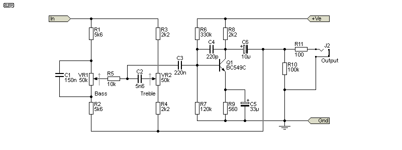
Figure 5 - Single Transistor Tone Control
An example circuit is shown above, using the same values as the opamp version. It's performance is not as good as the opamp, and as you can see it really does use more parts. That doesn't mean it's not useful of course, as it may be just what you're after. Unlike the opamp, power supply rejection is poor, so it may be noisy if you use a switchmode 'plug pack' (aka 'wall wart') external power supply. The filter circuit shown in Fig. 7 will help, but switchmode supply noise can be very difficult to filter out. When the tone controls are centred there's a slight loss of signal, but nothing to be concerned about (it's less than 1dB). As with the opamp tone controls, you can change C1 and/ or C2 to change the frequencies. The tone control amp as shown will draw about 1.8mA.
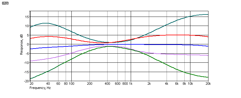
Figure 6 - Tone Control Response
The frequency response of the tone controls is shown above. The graphs were taken from the opamp version, but the single transistor version is very similar. With the controls centred, there's a slight loss of low frequency response (about 2.5dB) due primarily to the 10μF output cap from the booster stage(s). This is deliberate, as without limiting the extreme bottom-end, there's a risk of generating high amplitude infra-sonic content, which is undesirable. The response peaks at around 30Hz, and rolls off below that. The treble response is also intentionally limited, but it still extends to 20kHz.
The graphs are drawn for 0, 25, 50, 75 and 100% rotation, and the low frequency where the curves converge is done on purpose. Around 400Hz is much better for most musical instruments that the more typical 1kHz, corresponding to 'G' below A440 (which is roughly the physical centre of a full-sized keyboard). Of course, the frequencies can be modified by changing C1 or C2 in either of the tone circuits. Experimentation is encouraged, and you may find cap values that better suit your instrument and/ or playing style. Tone controls can be very personal, so it's worthwhile to experiment to find the combination that works best for you.
The DC input for pedals is something of a pain, because many are designed to use the centre pin for negative rather than positive. This appears to be historical, because when people started making pedals they used PNP germanium transistors, with a positive ground. PNP germanium devices were used because they had better performance than NPN types (this situation was reversed when silicon was adopted as the dominant semiconductor material).
Unfortunately, many DC input sockets have the metal body (which connects to the sleeve of the connector) grounded, so reversal of the input polarity requires the connector to be insulated from the chassis. This is usually harder than it sounds. There isn't any 'standard', so you can easily end up with a mixture of pedals - some with centre-pin positive, others with the centre-pin negative. The circuit below will not blow up if the polarity is reversed because of the input diode, but it won't work until the correct polarity is applied.
My preference is for the positive to be on the centre pin, as almost everything else that uses an external DC supply is wired that way. The DC input voltage can be anything from 9V to 18V. If you use other than 9V, it may be necessary to make adjustments to the circuits shown in Figures 2 and 6 to get optimal performance. The JFET circuit is adjustable, and the available range should be sufficient to set the drain voltages to roughly ½ supply voltage.
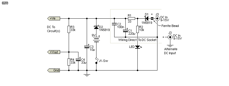
Figure 7 - DC Input & Filtering Circuits
The diodes and filtering shown are required for all variations shown here. The diodes protect against reverse polarity (D1) and stop an external supply from trying to charge the battery (D2). Some DC connectors include a switch to disconnect the battery, but many don't. The diode is easier to install, and there's less likelihood of an error when wiring the connector. The LED and its limiting resistor are optional. The LED should be a high-brightness type, as the current is deliberately limited to about 700µA.
The filter circuit is designed to remove noise from switchmode plug-pack ('wall-wart') supplies. The ferrite bead is optional but recommended - the type suggested is a miniature hollow core of around 5mm long by 4mm diameter. The nomenclature used by suppliers is inconsistent, but the dimensions will help you to find the right one. C2 is a 100nF multilayer ceramic, selected because they have good performance up to very high frequencies. As noted on the drawing, the filter network should be right next to the DC input socket, with very short wiring. C3 (10µF) is located on the Veroboard (or PCB if you make one), and bypasses the supply for the active circuits. This isn't shown on the individual circuits for clarity.
Vref (½ supply voltage) is only required if you use opamps, and the two resistors and the capacitor are left out if you use discrete circuitry. The Vref supply can handle both opamps in a dual package. It's a fairly high impedance for DC, but C4 ensures that the AC impedance is very low.
Beware: Many plug-pack/ wall-wart supplies are very noisy within the audio range when used at low current. The filtering shown may nor be sufficient to remove the noise, which may extend as low as 200Hz. This is caused by the SPMS entering 'skip-cycle' mode at low load so it draws almost no current from the mains. This problem came about due to government regulations demanding very low no-load power (typically 1W, sometimes less than 500mW, occasionally as low as 100mW). The regulators demanded this on the assumption that thousands (or perhaps millions) of supplies were left plugged in 24/7, regardless of whether they were supplying power to an external device. These MEPS (minimum energy performance standards) are worldwide (there are exceptions), and were the cause of the demise of transformer-based 'linear' power supplies. See Small Power Supplies Part III (section 6.1) for more details on this topic.
The circuit for bypass is shown next. It disconnects the electronics completely, so the signal will still get through even if the battery is flat or the external supply is faulty or disconnected. The disadvantage is that the guitar will have a much longer lead (two in series), and this may affect the tone (usually a loss of top-end). A simple buffer can be included between the output switch and output socket, but this will also stop if power is unavailable for any reason.

Figure 8 - Bypass Switching
This is operated by a DPDT (double-pole, double-throw, aka changeover) foot-switch. These are almost always 'push-on, push-off' types, and are used in countless pedal designs from many different manufacturers. Unfortunately, 3PDT (three-pole) switches are less common, so there's no way to switch an LED to indicate that the pedal is operating. Electronic switching (using a CMOS audio switch for example) will also work, but that adds complexity and it won't bypass with a flat battery or no power.
There are countless different ways to perform EQ for a guitar/ bass booster, but (for example) adding a 3-way parametric gets silly very quickly. You end up with so many knobs to control everything that the pedal becomes far too unwieldy and won't fit most pedal boards. A simple unit with gain, plus extra tone controls to 'help' the amp do what you need is usually quite sufficient.
I've avoided (well, not completely) guitar pedals since the ESP site was started. This isn't because they're not important or popular, but because I always figured that they were well catered-for elsewhere. There are literally thousands of circuits on the Interwebs, but the ideas here are at least capable of working as intended. I will always go for the opamp alternative when possible, because their overall performance is so much better than discrete circuitry, and most require fewer parts. An opamp such as the 4558 draws only around 2.5mA or so (typical), so there's little power saving to be gained with a discrete design (which can often end up drawing more than the opamp).
While my preference would always be for the opamp booster and tone control, not everyone feels the same way. There's also some satisfaction to be gained by building a circuit using discrete transistors, much of which is missing with opamp circuits. Yes, they perform better, but there are some for whom opamps are somehow 'not quite right'. There's no evidence that anyone will pick the difference between a well designed discrete circuit and an opamp in a blind test, but I've provided several solutions to ensure that constructors get the circuitry they prefer.
These circuits are not unique in any way, but they are designs that I know will work properly, and can be mixed and matched to suit your needs.
There are no external references, because the circuits are all adapted from other ESP designs, either in projects or articles.
 Main Index
 Projects Index