

|
| Elliott Sound Products | LDO Regulators |
 Main Index
 Articles Index
Introduction
1 - LDO Fundamentals
2 - Conventional Regulator
3 - Noise
Conclusions
References
Given the vast number of application notes, design guides and other material concerning low dropout (LDO) regulators, anyone would think they were complex. Despite initial appearances, they actually are complex. There are many things that must be considered to ensure stability, and not the least of these is due to the use of a PNP series pass transistor or a P-Channel MOSFET, which means the output is from the collector or drain, and not the emitter or source as with most conventional regulators.
This imposes several design constraints, and especially affects stability. In some cases, the output capacitor must be of a particular type, often one having greater than normal ESR (equivalent series resistance). Should you be sufficiently gung-ho and think that you can use any old cap you like, you may or may not get away with it. In many cases, the LDO simply becomes an oscillator, so rather than the nice clean DC you expect, you have DC, but with a high frequency superimposed. Adding more capacitance can make matters worse rather than better. These devices can be finicky, as a quick search through forum posts or application notes will confirm. There are some that are quite happy as long as a few basic conditions are met, but there are other LDOs that insist that you follow the maker's recommendations to the letter.
The circuits and results shown are exactly as simulated in each case. Note that these are not recommended circuits, but are simplified so that operation is easy to understand. While you probably could build them and get reasonable results, that's not the purpose here. This isn't a project or construction article, it's for information only.
The general scheme is shown (highly simplified) below. The output must come from the collector (or MOSFET drain) to ensure that the regulator can function with only a few hundred millivolts of input-output differential. Compare this to a conventional emitter-follower output, which needs an absolute minimum of around 1V, but more commonly 3 to 4 volts between the input and output. The reason for the voltage differential is quite simple. There has to be enough voltage across the regulator to ensure it can reduce the incoming DC to the value required, but all the while ensuring that there is a source of base current for the series pass transistor or gate voltage for a MOSFET. For a 5V regulator, that means that the input voltage has to be at least 7V, and usually more.
The two circuits that follow are conceptual - they both work in the simulator I use, and will (probably) work in practice as well. However, I don't suggest that you build them because they can never work as well as a commercial IC version. As should be apparent, the PCB real estate needed is significantly more than an IC too, as there are more parts used. Both circuits will have a -2mV/°C temperature coefficient because the emitter-base junction of Q3 is part of the voltage regulating feedback network. The zener diode will add more temperature dependence unless its voltage is around 8 volts where the tempcos cancel (zener diodes have a positive temperature coefficient above ~6.8V).
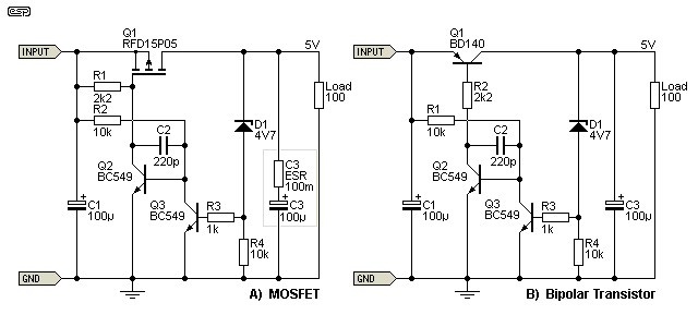
Figure 1 - Simple Discrete LDO Regulators (A - MOSFET, B - BJT)
The two versions function as follows ...
With a P-Channel MOSFET output device, the gate voltage is derived from the negative side of the supply, via Q2. R1 is needed so the MOSFET can be turned off. Normally, Q2 is turned on via R2, and when the output voltage is such that the zener conducts, Q3 turns on (slightly), removing some base current from Q2 and turning the MOSFET partially off to the degree necessary to keep the voltage at the preset level. The BJT version functions in a very similar manner, except that Q2 provides base current to Q1, rather than gate voltage. The base current is limited by R2 (2.2k in version B). If Q1 (BJT) has a gain of 50, the maximum output current will be about 120mA, but it varies with input voltage. In both circuits, C2 is a 'dominant pole' compensation capacitor, and it is required for stability (over and above other stability considerations).
For an LDO regulator, the necessary base current (or voltage for a MOSFET) comes from the negative supply (earth/ ground/ common). The series pass device can therefore operate with very little voltage across it. If the differential voltage is too low, the regulator will be less able to reject supply ripple. It's obviously a requirement that the lowest voltage (including negative-going ripple peaks) must always be greater than the output voltage.
Note the 100mΩ resistor (simulating a higher than normal ESR) in series with C3 in the MOSFET circuit. The gate-source capacitance of the MOSFET inserts another (unwanted) filter pole into the closed loop circuit, and without the increased ESR the MOSFET regulator is marginally stable. Small variations in components can trigger oscillation at the DC output unless the output cap has a higher than normal ESR. This is not an issue with the BJT version because the base capacitance is much lower than the gate capacitance of a MOSFET. This is exactly the behaviour that we need to be aware of. In practice, nearly all LDO regulators are fussy about the ESR of the output cap, and manufacturer's recommendations should always be followed. Using low-ESR caps is generally unwise.
The performance of the two is shown next, and the graph is for output voltage vs. input voltage at an output current of 50mA. The MOSFET regulator provides 5V out with only 5.05V in, while the BJT circuit starts to regulate with an input of 5.25 volts. The 4.3V zener may seem to have a voltage that's too high, but it operates at a very low current, and the voltage across it is lower than expected. Normally a precision voltage reference would be used here, such as a TL431 or similar. The zener was used for convenience when I set up the simulation.
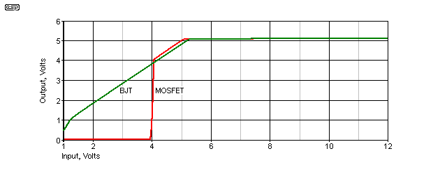
Figure 2 - Simple Discrete LDO Regulators Dropout Voltage (Red - MOSFET, Green - BJT)
With a MOSFET design, it requires enough input voltage to be able to turn on the MOSFET for the current needed. This may be 3V or more, and can be seen in the above chart - the MOSFET circuit has no output at all until the input has reached 4 volts. With a P-Channel device, the gate voltage is provided from the negative supply, and there only needs to be enough voltage between source and drain to ensure that the MOSFET has full control of the output.
A commercial LDO might be quite happy with no more than 100-200mV DC between input and output, so for 5V out, the input only needs to be perhaps 5.2V (depending on output current). This is a big advantage in battery powered equipment, because the battery can discharge to a much lower voltage before the regulator ceases to function properly. A standard emitter-follower based regulator can't come close to that, because apart from the emitter-base voltage, some additional overhead is needed to allow base current to be provided with minimal losses. This is a trade-off, in that allowing lots of base current at low voltages means high quiescent current at elevated voltages. The base current will usually be provided by fairly complex design to ensure that the regulator itself draws no more current than it needs to. This means a higher overhead voltage.
The next issue is output impedance. An emitter/ source follower has a low output impedance, even without feedback. Depending on the other parts used, an emitter follower can easily show an output impedance of less than 1 ohm. Conversely, the output impedance from the collector of a BJT or drain of a MOSFET is extremely high - typically several megohms. LDO regulators therefore rely on feedback to reduce the output impedance to something reasonable. Ideally, a voltage regulator has a zero output impedance, so that a change of load current does not affect the voltage. A simple emitter follower regulator (with no feedback) might show an output impedance of (say) 1 ohm, but LDOs will often struggle to get much below 0.5 ohm with feedback. They cannot be used without feedback.
As noted above, some LDOs are very susceptible to oscillation if the output capacitor has too much or too little ESR. A length of PCB track may introduce enough inductance to cause problems as well. Before you commit to using an LDO, you need to decide if that what you really need, and make sure that you follow the maker's recommendations to the letter. In some cases, that means using a 'high-K' ceramic capacitor of perhaps 10µF or so, and/ or using a tantalum capacitor (something to be avoided if at all possible IMO).
Because of the inherently high output impedance before feedback, if your load current changes rapidly over a wide range of current, you will need to use more output capacitance than you may have imagined. However, it must still fulfil the stability criteria for the LDO in all respects. It is useful that very high values of output capacitance (100µF or more) are usually less likely to cause oscillation than low values (see below).
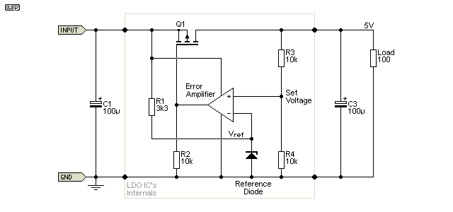
Figure 3 - 'Conventional' LDO Regulator Internal Representation
The drawings in Figure 1 demonstrate a simple discrete LDO, but a manufacturer's 'equivalent circuit' is going to look more like that shown above. The essential parts aren't really changed, but the error amplifier (Q2 and Q3 in Figure 1) is shown as an opamp. In reality, the internal circuit may (or may not) be very different from the discrete circuits above, but even the equivalent circuit here is a simplification. There will be provision for short-circuit protection, over-temperature shutdown, and other functions that vary from one device to the next. The voltage setting components (R3 and/ or R4) will be external for adjustable types.
The idea here is to show the basics, primarily from the perspective of stability. The following chart is adapted from Texas Instrument's SLVA115 [ 4 ] for the TPS76050 LDO voltage regulator IC. It shows the range of output capacitance vs. ESR that ensures stable (or unstable) operation. This general trend is very common, although the specifics vary depending on the LDO. Some LDO regulators may even need a low value resistor in series with the output cap to ensure stable operation. Note that it is equivalent series resistance (ESR) that can be critical, not the value of capacitive reactance, which of course falls with increasing frequency. In some cases, ESL (equivalent series inductance) may also be an issue, but few bypass caps have more than a few tens of nano-Henrys of ESL at the very most. It can be significantly less than 10nH for most SMD caps. PCB tracks can add a lot more. For reference, 10mm of straight 0.1mm wire has an inductance of about 10nH.

Figure 4 - LDO Regulator Stability Vs. Output Capacitance
As is obvious, if you were to use a very low ESR 10µF capacitor (e.g. some multilayer ceramics), the circuit will oscillate, as it's in the 'unstable' region of the graph. You would need to ensure that a 10µF capacitor had an ESR of at least 100mΩ to remain well within the 'stable' section. Larger value caps have a bit more leeway, but a 2.2µF cap is marginal regardless of its ESR. The stability can also be affected by load current, so it is essential that you are fully acquainted with the requirements of the LDO you plan to use before you choose the support components. Ensuring that the capacitance and ESR remain stable over the long term is also important, so capacitors have to be chosen with care. You also need to be aware that high-K ceramic dielectrics also suffer from capacitance loss due to aging (time and temperature).
There are significant risks when using 'high-K' ceramic caps (common in SMD), as most have a significant voltage coefficient, and can lose 50% or more of their stated capacitance just because they are operated near their rated voltage. These caps also have a high thermal coefficient, so have to be tested over the full temperature range. Much as it pains me to have to say so, sometimes tantalum is the only sensible option for the output cap. I have avoided them for many years because of their undesirable characteristics (not the least of which is 'exothermic ignition failure' - they can (and do) catch on fire!). However, sometimes nothing else provides the specific conditions needed for stability [ 5 ].
Most articles will go into some detail about the filter poles that exist within the LDO itself, and the additional pole created by the output cap. Phase diagrams and other details are often very helpful for those who fully comprehend the closed loop stability criteria for feedback circuits, but the datasheets usually provide the specific information you need to ensure that you don't build an oscillator. Full phase analysis is not essential, but it is important to know that problems will be created if you don't follow the recommendations.
Bear in mind that it's not just the cap at the output of the LDO regulator itself that must be considered - bypass caps across the supply lines of ICs that the circuit uses are also part of the output capacitance, and may cause unforeseen problems if you are unaware of this.
For some perspective, the drawing below shows a simple discrete 'conventional' (emitter follower) regulator. This will be stable with almost any imaginable combination of output capacitance, and used to be a very common design before the advent of 3-terminal regulator ICs.
If the transistor is NPN (and assuming a positive regulator), the base current has to be supplied from the input. That means the input must be at least a couple of volts higher than the base of the series pass transistor, and the emitter (the output) is 700mV lower than the base voltage. The circuit shown below will normally be unconditionally stable with any value of output capacitor, and ESR is usually irrelevant.
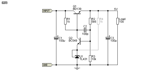
Figure 5 - Simple Discrete Conventional Regulator
The output is from the emitter of the series pass transistor (Q1). Should the output voltage rise above the preset voltage, Q2 is turned on a little harder via R2, causing it to 'steal' base current from Q1, which turns off just enough to keep the voltage steady. The reverse happens if the output voltage falls. If a zener diode is used for the reference, it should get most of its current from the regulated output (via R4), ensuring a stable output. This is not required if a precision reference diode is used. The version shown is hampered somewhat by its (deliberate) simplicity. This type of circuit was commonly used with output voltages of 12V or more, and weren't normally used for 5V supplies in the general form shown. The main reason for their use was to minimise ripple - there was rarely a need for a very accurate regulated supply.
The circuit is the basis of the regulator shown in Project 96 (48V phantom feed power supply), and this topology was used because it can withstand a much higher input voltage than a 3-terminal regulator. This basic circuit can have surprisingly good performance with a few additional parts, but these days it actually costs more to make than it does to buy a 3-terminal regulator, which outperforms it for most tasks. (It's still useful for high voltages though.)
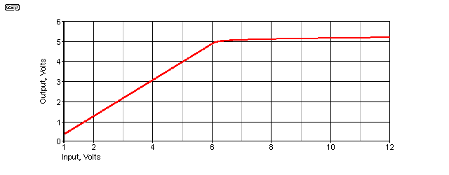
Figure 6 - Discrete Regulator Performance
The performance of the regulator is shown above. It's not as good as the LDO versions shown above because it has lower gain. Ideally, R1 would be replaced by a constant current source which improves the circuit's regulation markedly - but also increases complexity. However, it shows the principle, and it's obvious that it can't start regulating until the input voltage reaches 6.2V, over 1V more than the LDO type. In most circuits, the required differential is higher than this - in general, assume that the input should be at least 3V greater than the regulated output.
Like any other active device, regulators make noise. Because of the way LDOs are so often used (at low voltages and with sensitive analogue to digital converters for example), noise can cause problems. It's important to distinguish between internal noise (including the noise contribution of resistors used to set the output voltage) and power supply rejection ratio (PSRR). Supply ripple rejection is usually not an issue with a battery powered or a pre-regulated supply, such as a 3.3V supply derived from a regulated 5V source.
Internal noise includes thermal, flicker (1/f) and shot noise. The most significant contribution is usually from the band-gap used to provide the reference voltage, and while it's difficult to get a straight answer from most of the published material, it would appear that LDOs are generally quieter than conventional regulators. Comparing quoted output noise figures isn't always easy, because they are often specified (very) differently.
As an example (directly from datasheets), the LM317 adjustable (conventional) regulator has a noise figure of 0.003% / V output, while a TPS76425 (2.5V) LDO has a noise output of a little over 60µV with a 10mA output current. Noise increases with increasing output current. Specifying the output noise in completely different ways doesn't help anyone - if you work out the noise for the LM317 at 2.5V output, it's 75µV.
When it comes to determining the actual amount of noise generated by the regulator, you need to consult data sheets, and/or put one together and measure it. This is a surprisingly complex area, and doubly so with LDOs, because noise often varies with output voltage as well. Noise is a particularly important parameter for LDO regulators because of the way they are used. The output voltage is usually low, with 5V being towards the upper end of where they are typically used.
Because LDO regulators are common with sensitive electronics (especially ADCs and DACs), noise performance is critical to the performance of the circuit being powered. Unlike opamps which have very high power supply rejection, most ADCs and DACs rely on the supply being noise free to ensure an accurate (and hopefully low noise) output.
In this short article, I have tried to highlight the potential issues with LDOs, especially compared with 'conventional' voltage regulators. There is no reason to be put off using one if that's what your circuit requires, but if you have plenty of 'spare' voltage available (such as with most mains powered power supplies) then a conventional voltage regulator is almost always a better choice.
LDOs can be finicky, and because of their topology they are not inherently stable. It's certainly possible to make a standard regulator oscillate too, but it usually requires rather sub-optimal (or simply misguided) design and PCB layout to cause issues. With an LDO, you could easily run into trouble just by using an output capacitor that's different from the one that was used for initial tests. It's also necessary to ensure that the capacitor used will not degrade over time in such a way as to cause problems after a few years of operation.
It's a clear sign that a part is likely to be tricky to use when manufacturers offer evaluation boards. You won't find any for conventional regulators, but there are many available for LDOs, with most provided by the manufacturers and/or major distributors. Provided you follow the maker's guidelines and test the design thoroughly, there is no reason not to use an LDO if that's what you need, but as I hope is now obvious, they are not as predictable as the 3-terminal regulators you are used to.
For battery powered circuits, the LDO is by far the best solution unless there is already a higher voltage supply available. For example, a circuit using a combination of analogue and digital circuitry might need 11.1V (LiPo, 3 cells in series) for the analogue side (typically opamps) and 5V for the digital side. An LDO isn't needed here because the main supply can't be allowed to fall below around 9.5V to prevent battery damage, so there is still plenty of headroom for a standard regulator. If you need 3.3V from a single LiPo cell, then you have no choice.
 Main Index
 Articles Index