
|
|
| Elliott Sound Products | Using HEXFETs in High Fidelity Audio |
 Main Index
Articles Index
Main Index
Articles Index
When we build linear power amplifiers, we always need to choose some device for the output stage. This could be any power device including valves, BJTs, IGBTs, and MOSFETs. Each has its own strengths and weaknesses which forces us to choose between them. If, perchance, we wanted to build a very simple and accurate amplifier, we can safely ignore valves, since they all need heating circuitry and are not simple for a true hi-fi amplifier. That it is possible to build a valve amp to a high specification is not in doubt, but they tend to be complex and expensive.
BJTs are often used, but they do not respond well to even momentary overloads. This is because they suffer from second-breakdown - an instantaneous and catastrophic failure mode. IGBTs (Insulated Gate Bipolar Transistors) are seldom used, and will be very similar to a BJT, only with an insulated gate. They still need thermal compensation and a suitable gate drive design, and can suffer from a 'latch-up' condition in some cases. Lastly there is the MOSFET, which does not suffer any second-breakdown effects (although this is not strictly true - see below for more info). MOSFETs (Metal Oxide Semiconductor Field Effect Transistors) come in two primary types - vertical and lateral.
These devices are extremely rugged, yet they do have a large nonlinear gate capacitance to deal with. If driven incorrectly, they show high distortion levels, especially vertical types - most commonly these days, HEXFETs. This is why I wrote this article - to show how to use HEXFETs properly in audio applications.
The update below has some important information that I recommend you read thoroughly and make sure you understand before settling on the use of HEXFETs in your next amp project. While there appear to be many advantages to their use over BJTs, HEXFETs may often suffer from exactly the same problems - thermal runaway and a failure mode that is suspiciously similar to second breakdown. On top of this, there is a much larger voltage loss ... 2-4V is needed to bias the HEXFETs to the on condition, vs. 0.65V (nominal) for BJTs. This voltage is usually taken from the main supplies, so for a given supply voltage, expect a little less output power.
Many people say (including IR) that HEXFETs are not suited for linear audio circuits and should be avoided. Well, that is the easy route to take for designing an output stage. Any device can be used for audio and give great performance if a proper design is found. It is just easier to use more linear devices. Lateral MOSFETs are usually specified for audio, but there are relatively few different devices on the market. When found, they tend to be quite expensive. On the other hand, HEXFETs are very common, reasonably priced, and only need a good design to do well.
This article is intended for Class-AB designs. HEXFETs will run Class-A with barely any problems besides driving the gate. If you are designing a class A amplifier, the first trick (see below) should be used (the second is not needed since the bias is already quite high).
Alright, now for some explanations. Comparatively, HEXFETs usually have a low gate capacitance than other vertical MOSFETs, yet have a higher gate capacitance than their lateral counterparts. There is not only one capacitance to deal with, but two (one from the gate to source and the other from the gate to drain). This is the main problem: to find a way to drive the gate capacitance of the HEXFETs. Through a lot of time and molten breadboards, I found the best two things to design for are the following:
1 Fix: Drive the gates with as much current as possible. This may include adding a class AB driver stage. Why: HEXFETs have a nonlinear transfer curve up to about an amp or two, depending on the device(s) used. In a class AB amplifier, this characteristic is the cause for a majority of the THD. When driven with enough current, the device will follow the 'new' linear curve, since it is balancing out the nonlinear gate capacitance. The lower impedance of the driver stage the better. 2 Fix: HEXFETs like to run hot. This does not mean use an inadequate heatsink, but the bias between devices should be a bit more than many are used to. 250mA of idle current is not a bad bias figure for these devices. Why: To balance out the nonlinear curve, we can simply cut if off where it seems too bad by using bias. This will increase dissipation, though.
For the design of the amplifier, I will assume a single LTP input stage. Better performance can be seen by using multiple LTPs, but this will not be a simple design (in fact it will be quite complex with high frequency stability issues needing attention).
When choosing the complementary output components, one can obviously choose the IRFPxxx and its IRFP9xxx complement. If we look at these complementary device data sheets, we will see very different figures for current capability, on resistance, and, most importantly, gain (or forward transconductance). But if we use a matching tool, we will find that the gain varies considerably from the actual devices vs. the data sheet. That is why we need to buy a few extra and match them together. Since the gain varies a bit from batch to batch, it is quite easy to find a IRFPxxx and IRFP9xxx that are very similar, at least with gain factors.
Also take note that HEXFETs will require a Vbe multiplier for thermal compensation, since the negative temperature coefficient does not come into play until the device has about 10 amps through it (at least for the IRFP240). The exact values around the Vbe multiplier (also known as a bias servo) are critical to ensure that the thermal performance is matched as closely as possible.
In every practical design I have tried I had to use a class AB driver stage. A class-A driver will work fine if you really want an electric heater, as you will see in the next calculation. Now, in order to size-up the proper driver for the FETs, we need to do a little maths. I promise it is not hard. An example would work nicely here ... if we wanted to design a class AB driver stage with five IRFP240 and five IRFP9240 devices, how much current will we need at minimum for full functionality up to 50kHz? For a better understanding, a simplified output stage circuit is shown below.
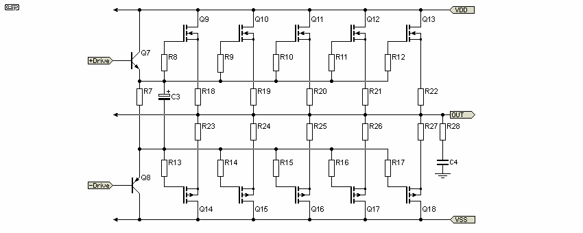
Figure 1 - MOSFETs and Driver Circuit
We will do calculations using the gate charge method, which IR recommends (AN-944). Looking at the data-sheets, we find the IRFP240 has a total gate charge (Qg) of 70nC and the IRFP9240 has a Qg of 44nC. Don't add these yet! We will find each device's needs individually. The general formula to determine gate current is ...
I = 100Qgf where I is current needed, Qg is the total gate charge in Coulombs, and f is frequency of operation.
The multiplication factor of 100 gives the headroom needed for accurately reproducing a square wave (or high frequency sinewave), since the gate driver needs a lot of current to quickly switch the MOSFET from OFF to ON. Although the requirement for this is minimal (the CD format is incapable of anything even approaching a square wave above a couple of kHz), it has become an expectation that power amps should be able to reproduce perfect square waves at 10kHz as a minimum.
When we plug our figures in for the IRFP240, we get I = 100 * (70E-9 * 50,000) = 350mA per device
For the IRFP9240 we get I = 100 * (40E-9 * 50,000) = 200mA per device
Multiplying each figure by five (because there are five devices of each polarity) gives us 1.75 amps for the upper driver and 1 amp for the lower driver. So a Class-A driver would need bias set to 3.5 amps to get the job done with a reasonable safety margin.
The value for R7 will depend on the linearity of the driver transistors. I had to guess and check with my ammeter to get a good value. This can range anywhere from 100 Ohms up to perhaps 5k. Make sure you check the idle current before calling the design done! These drivers (Q7 and Q8) may need a heatsink. Also note the capacitor in parallel with R7. This should be of a high value (e.g. 100µF or more), and 470µF works fine for my 10 MOSFET stage shown here. It helps with discharging the MOSFET gates by providing a path for the gate current.
These current figures seem quite high, but keep in mind this current will only last a very short time compared to the signal, and virtually no current is needed to keep the devices either in the OFF or ON state. The current to reproduce a sinewave will be a bit lower, since it is a smooth curve, but this much headroom will drastically lower distortion. This is why we cannot practically use a class A driver, unless, of course we use one pair of output devices.
For some comparison, below is a HEXFET setup driven by a class A driver at 13mA bias:
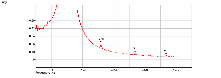
Figure 2 - Spectrum of HEXFET with 13mA Class-A driver
The large notch is at the second harmonic, and the small bump to the right is the fourth harmonic. Barely any third harmonic is seen. This shows 0.25% distortion at the second harmonic at ¾ power, and 250mA amp bias. Not very good for a true hi fi, unless we are making a valve-like amplifier. Even this will not show the same effects as a true valve amp - the nature of the distortion components will almost certainly be different.
Adjusting the bias to 1 amp removes nearly all distortion, yet now we are approaching a heater ... I mean class A.
After fixing the problem by adding a class AB driver, distortion was greatly decreased ...
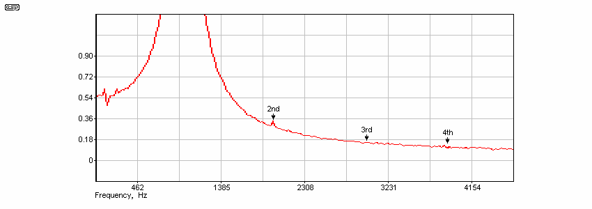
Figure 3 - Spectrum of HEXFET with Class-AB driver
As the picture shows, the second harmonic was reduced considerably, while the fourth harmonic is below the noise floor. This shows 0.04% distortion solely on the second harmonic at ¾ power and still with 250mA bias. This greatly improved the amplifier. At one watt, the distortion is not measurable at all, unlike with the class A driver. Reducing the gate resistors to 4.7 Ohms to get more current through does nothing noticeable, so the use of 10 Ohm resistors is fine. There is no evidence of 'notch' distortion or any other nasty odd harmonic, only a 'nice' second harmonic added in. Also note that this amp was built on a breadboard. A compact and nicely wired PCB should decrease distortion even further.
Below is the final simplified schematic of the entire amplifier ...
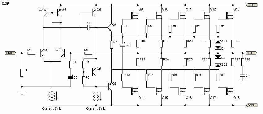
Figure 4 - Simplified Schematic of Complete HEXFET Amplifier
It looks very simple, and includes the Class-AB driving stage to improve gate driving. It's very simple compared to amps with multiple LTP stages. The minimum stability network (Zobel) shown is always needed, and a series inductor (with parallel resistor) may also be required. The values of these components will be found by experiment.
For some further reductions in distortion, the following work quite well:
HEXFETs are decent devices once the gates are driven correctly. They are much more rugged than BJTs as my burned parts pile shows, and sound very good when a class AB driver is added. I hope this short article with aid others in using these 'switching' and 'not linear enough for audio' devices to get distortion figures below many good amplifiers with 'very linear' devices. And remember one thing - any output device can be precise if a proper design is found. Finding the correct design parameters becomes more complex with non-linear devices.
The following are all PDF files, and are direct links to the International Rectifier web site ...
IRFP240 data sheet
IRFP9240 data sheet
AN-936 application note - The Do's and Don'ts of Using MOS-Gated Transistors
AN-937 application note - Gate Drive Characteristics and Requirements for HEXFET® power MOSFETs
AN-941 application note - Paralleling HEXFET® power MOSFETs
AN-944 application note - Use Gate Charge to Design the Gate Drive Circuit for Power MOSFETs and IGBTs
AN-948 application note - Linear Power Amplifier Using Complementary HEXFET Power MOSFETs
... And many pages from ESP
The above article is a contribution from Mitch Hodges, and ESP has not verified all aspects of the design process described. While the circuit can be (and has been) simulated quite readily with good results, this is no guarantee that everything will work as expected. I added diodes and zeners to protect the MOSFET gates from excessive voltage. It may be possible to select the zeners to achieve basic current limiting, giving the amp some protection from overload conditions. Because of the high gain of HEXFETs, this simple protection scheme will not be particularly effective. Also, remember that a series inductor may also be required.
It will be noted that there are no component values supplied - this is quite deliberate, and is not an omission. The article is intended to describe the design process and how to work around the inherent non-linearity of vertical MOSFETs, and is not intended to be a construction project. Requests for component values will not be fulfilled.
It must be understood that at the suggested current (250mA per MOSFET pair), the total quiescent current will be in the order of 1.25A - at a typical supply voltage of perhaps ±50V, this represents a total quiescent dissipation of 125W! This is a formidable amount of heat to dispose of, and will require very large heatsinks (and/ or forced air cooling). It is probable that the constructor will be forced to compromise, using a significantly lower quiescent current than suggested just to maintain a sensible heatsink size and temperature. Reducing your expectations of the maximum frequency that needs to be passed at full power will reduce the loading on the Class-AB drivers, but does nothing for the MOSFET low current linearity. Compromise will be almost essential (IMO).
Finally, I'd like to thank Mitch for his contribution, since it describes the issues and how to solve them in an easy to follow manner, keeping complexity to the absolute minimum in the final design example.
Rod Elliott
I have had occasion to build a HEXFET based power amp as a test for a client. While it worked well enough, giving the expected power output and with fairly low distortion, as noted above the required bias current is quite high to reduce crossover distortion to an acceptable figure. While the circuit I built was actually quasi-complementary (using only N-Channel MOSFETs), the basic principles apply regardless.
As it transpires, the design I was looking at was unsuitable for the intended purpose, because the quiescent current needed to remove crossover distortion was too high to be practical. In many cases, the lowest heat output possible is highly desirable, and HEXFETs are simply unsuited to any application where very low Iq is desirable or necessary. Lateral MOSFETs would be fine, but are too expensive for my customer's application (in case anyone was wondering).
Bias stability is definitely an issue as discussed above. It is commonly (and erroneously) stated that MOSFETs are 'safe' because they have a positive temperature coefficient, so as a device gets hotter, its drain-source (RDS(on)) resistance increases. This much is true, but this alleged 'benefit' is actually completely useless in a linear circuit. (It can also cause major problems in switching circuits, but that's another topic altogether and will not be covered here.)
What is not commonly noted is that all MOSFET devices have a fairly high negative temperature coefficient for the gate-source threshold voltage (Vth). At the gate-source voltages needed to obtain typical bias currents, even a small temperature increase causes a large drain-source current increase, so the use of a carefully designed bias servo (Q5, R5 and R6 in the Figure 4 schematic) is absolutely essential. This point is made above, but is sufficiently important that repetition will not go astray.
To illustrate this, Figure 5 shows the graph from the IRF540 data sheet, and although it does not continue down to the levels we are interested in, the trend is clearly visible. At a VGS of 4.5V, we see ID of around 12A at Tj = 25°C, rising to a little over 20A at Tj = 175°C. While the graph might seem to indicate that the effect will be greatly exaggerated at lower gate voltages and drain-source current, the initial tests that I did indicate that the effect is roughly similar. The graph was taken from the IRF540 data sheet, but has been colour coded to make identification of each graph easier. The use of source resistors to help force current sharing is essential, and these should be as high as practicable. While 0.1 ohms is common for BJT amplifiers, I would recommend values not less than 0.47 ohms for HEXFETs. Higher values provide more stable quiescent current with temperature variations. For example, with 1 ohm source resistors, the current can increase at a maximum of 1mA/mV or 1A/V. Should Vth fall by 100mV, Iq can only increase by 100mA. This eases the design of the bias servo.
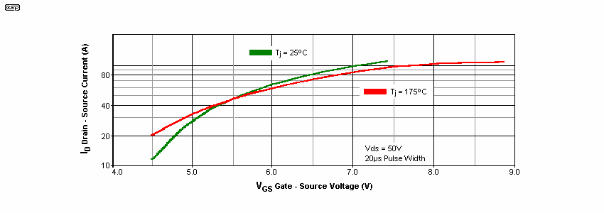
Figure 5 - Temperature Coefficient, VGS (IRF540)
The test I ran was very simple. Apply a suitable voltage to the drain, then carefully adjust the gate voltage until a suitable measurement current was drawn. The current started at a relatively low value (around 1A in my test), and as the device heated up this was seen to rise. It stabilised fairly quickly because the heatsink prevented further (possibly damaging) heat levels, but with two MOSFETs in parallel, the current between them was different, and (more importantly) it remained different, even as they became hotter. The claims for better (and 'automatic') current sharing apply only to devices operated as switches, or where the two curves shown in Figure 5 cross over each other. Only lateral MOSFETs provide a crossover point on their transfer characteristics that is low enough for linear operation.
Something that is missing from nearly all MOSFET data sheets I have looked at is gate threshold voltage vs. temperature, although it is shown in the data I have for the IRF840. This will show that the threshold voltage falls as Tj increases - a negative temperature coefficient. The positive coefficient of RDS(on) is insignificant at the current levels needed for setting quiescent current accurately. Note that the two curves cross over, but the point where the temperature curves cross is when VGS is at a current of over 40A and the gate-source voltage is 5.5V - this is not useful. Lateral MOSFETs (as used in P101) have exactly the same issue, but the curve changes from negative to positive at a much lower current (around 100mA), and this is visible on the transfer characteristic graph (but you will need to look for it carefully - it is not specified in a useful manner IMO).
In an application note [ 1 ], OnSemi describe this transition as the 'inflection' point, and it is determined by VGS, although it appears to be related more to the drain current than gate voltage. However, the two are directly related, so the point is moot. Lateral MOSFETs are usually quite safe here, because the inflection point is at such a low voltage and current, but vertical MOSFETs (HEXFETs and similar) are prone to thermal runaway. There is also the possibility of a failure mode very similar to second breakdown when HEXFETs used in linear circuits, where VGS is usually (well) below the inflection point. This must remain a very good reason to stay clear of these devices for audio, unless you are fully aware of the potential risks, and how to avoid them. Note that the article above does not address this potential failure mode, (nor do many others), and your only choice is to find MOSFETs where the thermal 'changeover' occurs at the lowest possible drain current. Lateral devices are almost unbeatable in this respect.
A careful examination shows that the 'inflection' point is actually the region where the negative temperature coefficient of VGS exactly compensates for the positive temperature coefficient of RDS(on). That's the reason it's at such a high current for HEXFETs (because of the usually low RDS(on) value), and it is known that the inflection point is inversely proportional to RDS(on). Note that this only applies if the device is used in linear mode. When switching, Vth and its temperature coefficient is not relevant because the gate voltage is invariably selected to provide 'hard' switching to minimise losses.
In contrast, a typical lateral MOSFET (such as the 2SK1058) has an RDS(on) of around 1.5 to 1.7 ohms at ~10A, compared to an IRF540N with 0.044 ohms at 16A. When choosing HEXFETs for use in linear circuits, I suggest that you use devices with the highest value of RDS(on) that you can find. This is entirely counter-intuitive, and is almost certainly the exact opposite of what you would expect. RDS(on) is actually meaningless in a linear application until the amp starts to clip, and even then only reduces the maximum output power slightly. As a figure of merit, it only has meaning for switching applications.
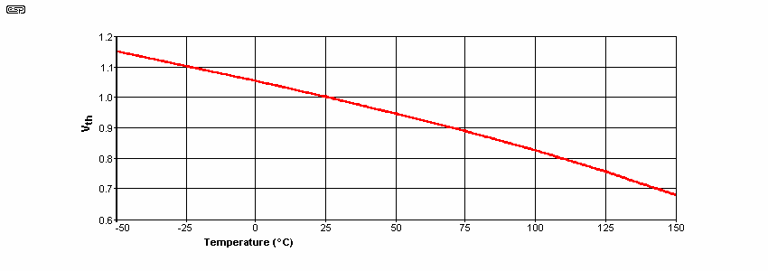
Figure 6 - Normalised Vth Vs. Junction Temperature
From Advanced Power Devices, their application note [ 2 ] provides the graph shown in Figure 6. Normalising simply means that everything is taken back to a reference of unity, so simply multiply the claimed Vth by the figure shown along the left side, for the temperature at which your device will operate. If your MOSFET will undergo a temperature change from 25° to 100°, then Vth will fall to 0.83 of the ambient temperature value at 100°C. This application note also mentions the possibility of a failure mode similar to second breakdown when operating switching MOSFETs as linear amplifiers. The App. Note refers to this failure mode as 'hot-spotting' or 'current tunnelling', but it's very similar to traditional second breakdown. Indeed, two of the articles listed below refer to the fact that using a HEXFET much bigger than needed (to provide a safety margin) has exactly the opposite effect. Rather than increasing the safety margin, the larger device is more likely to fail if it is working well below the 'inflection' current in a linear circuit.
Do not be mislead by claims that MOSFETs are immune from thermal runaway, although lateral MOSFETs are much better in this respect than vertical MOSFETs (HEXFETs and similar high-gain switching devices). Based on the above, it is quite apparent that vertical MOSFETs can easily get into thermal runaway if the bias servo is not set up correctly. Using just a pot (as shown in P101) is absolutely forbidden with vertical FETs - a matched bias servo thermally coupled to the MOSFET heatsink is essential to prevent both thermal runaway and crossover distortion.
Further searching revealed a document from Solid State Optronics [ 3 ], where the temperature coefficient for VGS is said to be -1.5mV/°C (the above chart shows it as 1mV/°C for VGS of 4.5V at 25°C). It is claimed to be 'insignificant', and for switching applications this is true. It is definitely not insignificant for a linear circuit (as shown in Figure 4), and especially so because of the relatively high transconductance of vertical MOSFETs. A few (tens of) millivolts of gate voltage is the difference between acceptable quiescent current and overheating.
What of the second breakdown effect that the manufacturers deny even happens other than in the (very) fine print? HEXFETs, and indeed most other MOSFET devices, are made using a multiplicity of individual small MOSFETs called cells. If the device as a whole exhibits a negative temperature coefficient for VGS, so must each internal cell. If one cell has a slightly lower VGS than the others (perhaps due to microscopic variations in the silicon) it will take more of the total current. This will cause it to get hotter, so the threshold voltage will fall further and it will then draw more current, causing it to get still hotter. This process continues until the cell fails due to over temperature, at which point the MOSFET suffers catastrophic failure.
While this scenario is not common in switching application, if the MOSFET is used linearly it is very real, and has caused problems in the past. It will continue to cause problems if designers are unaware that this failure mode even exists - after all, most comments seen describe MOSFETs as almost indestructible. While this is true to an extent, it is obvious that it is not a general rule upon which one should rely in all circumstances. HEXFETs operated in linear mode need to be derated from the claimed maximum dissipation, and my suggestion is that a maximum of half the rated power dissipation is reasonable. Likewise, the peak current should also be much lower than the rated maximum.
Now you know why International Rectifier and other vertical MOSFET manufacturers don't recommend HEXFETs or their equivalent for linear applications - they are simply not designed for the purpose. Yes, they most certainly will work, but you must be aware of the limitations. I suggest that high voltage, relatively low current devices are preferable to the reverse, as they will have an inherently higher RDS(on), and therefore a lower inflection point. Alternatively, you can look for 'vertical' MOSFETs that are specifically designed for linear operation. They exist, but are probably considered 'exotic' by most suppliers. An example is the IXYS IXTK22N100l (with 'extended' FBSOA), but at over AU$70 each (one off price) when I looked most people will think that's a bit rich.
Toshiba used to make vertical MOSFETs that were designated as being suitable for audio amplifiers. The 2SK1530 and 2SJ201 were basically switching devices, but with a comparatively high (but unspecified) RDS(on) of between 0.3 and 0.6 ohms. I've tested an amplifier that used them, and they perform well enough, but it's doubtful that there was really any advantage over using bipolar output transistors (other than cost). These devices are now obsolete, but they were classified for VGS(off), with '0' classed devices having a threshold voltage of 0.8-1.6V, and 'Y' class with 1.4-2.8V. This was unique amongst MOSFETs, and I don't know of any other MOSFET type that has provided a degree of 'pre-matching' when you buy them.
If you intend to use vertical MOSFETs for any linear application, you need to be aware that the published SOA curves do not apply to linear operation. Feel free to read that again to make sure that you understand the ramifications.
There's little or nothing in the datasheets to warn you, and many data sheets even show the SOA for DC. A few careful calculations will show that there is no way that the MOSFET can be operated at full rated power while keeping the die temperature below the absolute maximum (typically 175°C). The only way that you can be assured of safety is to keep the peak dissipation well below the claimed maximum, thus minimising the die temperature. This is a minefield, and I suggest that you tread very carefully. See the IR application note for more detailed information [ 4 ].
Interestingly, some of the earliest MOSFET fabrication processes are less likely to fail if used in linear mode, because they have a comparatively high RDS(on). However, most of the early types are obsolete, and their nominal replacements are 'better' in that RDS(on) is lower than the previous version(s). While this is good for switching (reduced losses), it also ensures that they are less suited to linear operation.
It's worth looking at RDS(on) for lateral MOSFETs as a point of comparison. The figure isn't quoted, but it can be calculated using the Drain-Source saturation voltage figure provided. VDS(sat) will normally be in the order of around 12V (gate shorted to drain) at a current of 7-8 amps, so RDS(on) is in the order of 1.5-1.7 ohms! Compare that with the figures you see for HEXFETs - the IRFP240 has an RDS(on) of 0.18 ohm, but it's also important to understand that completely different test methods are used so a direct comparison isn't as easy as it seems.
Another specification you can look at is 'Forward Transfer Admittance' ( |Yfs| ), aka forward transconductance in Siemens. Lateral MOSFETs have a transconductance of 1.7-2.0S, while even most high RDS-on vertical/ HEXFETs have a transconductance of at least 5S, and the latest models are much higher. Early MOSFETs were much easier to use in linear circuits than new ones, because they had lower transconductance and higher RDS-on.
One thing that is a dead giveaway as to whether a MOSFET is lateral or vertical is to compare the pinouts. Lateral MOSFETs have the source pin in the centre, while vertical types invariably have the centre pin as the drain. Many fake lateral MOSFETs are re-badged vertical devices (typically HEXFETs), so source and drain are in the wrong places and the amp will provide close to a dead short across the power supply via the intrinsic body diodes.
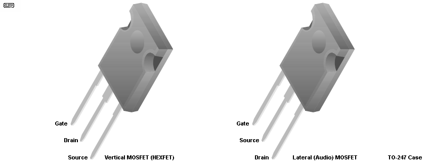
Figure 7 - Vertical Vs. Lateral MOSFET Pinouts
As far as I'm aware, there are no exceptions to the above. There are no lateral MOSFETs in the TO-220 case that I'm aware of, and all true lateral high-power MOSFETs use the TO-247 case or a small variation thereof (TO-3 lateral MOSFETs may also be available, depending on supplier). It's worth noting that the TO-220 package is useless (regardless of what's inside) for getting rid of any more than about 20W worth of heat, unless extraordinary care is taken with mounting.
As should now be quite obvious, it's very hard to recommend using HEXFETs in an audio amplifier. Mitch has made a compelling case, but much has changed since the article was written, and there is also more information available. This won't stop people from trying, because HEXFETs are cheap compared to lateral MOSFETs and high power bipolar transistors, and seem to offer many advantages. As is now clear (I hope), most of the 'benefits' are an illusion, and can easily lead to tears if the warnings here aren't heeded.
1 On Semiconductor - AND8199
2 Advanced Power Technology - AN0002 - no longer found at the source, but now available from the ESP site
3 Solid State Optronics - Application Note 50
4 International Rectifier - AN1155
Main Index
Articles Index