
|
|
| Elliott Sound Products | Class-G Amplifiers |
 Main Index
Articles Index
Main Index
Articles Index
Firstly, there is some dissent as to what constitutes Class-G compared to Class-H. I have explained the difference as I see it below, but there are many amps that claim to be Class-H that I consider to be Class-G. Because neither class is 'officially' recognised (as are Classes A, B C & D) it becomes a moot point. Ultimately, it doesn't matter all that much, so feel free to consider the two terms to be interchangeable.
Many people will have noticed that most of the professional high-power amplifiers made these days are Class-G, and seem to have remarkably little heatsinking for the claimed power output. Should one look inside, there are more output transistors than expected too. As well, you may notice that there are also many more diodes than you'd expect to find in any 'normal' amplifier.
All very baffling, and especially so since there is so little information on the Net about Class-G amplifiers. There are almost no schematics that are more than a basic concept, so figuring out how they work is not easy. While a very few circuit diagrams can be found in manufacturers' websites, for the most part it seems that there's a conspiracy of silence surrounding these amps. Without a full service manual, the likelihood of most people finding a complete Class-G schematic are fairly limited.
Certainly, they are discussed (or in some cases simply dismissed [ 1 ]) in various books on audio amplification, with varying opinions as to their suitability, sonic qualities, etc. One thing is quite clear - the added complexity is only of benefit for high powered amplifiers, having an output power of 200-300W or more. In addition, the use of Class-G is of dubious value for normal home listening, where the average power may only be a few Watts but instantaneous (peak or transient) power may reach far higher levels. Although there are modest gains in efficiency, they do not warrant the additional complexity.
At the modest power ratings generally needed for home use (generally well below 200W per channel), a traditional Class-(A)B amplifier is perfectly capable of providing as much noise as you'll need, without raising a sweat. In addition, the lower complexity reduces the likelihood of distortion artifacts, which (it is claimed) may become audible in some (others may say all) Class-G designs.
Despite the so-called 'failings' of Class-G, the technique is now being used for high-speed ADSL line drivers [ 2 ] . This is a surprisingly demanding application, and that the benefits were seen as worthwhile and the apparent limitations (marginal dissipation improvement, distortion) of little concern, some people take the technique very seriously indeed. The other benefit is that the power transformer may be physically smaller, although more complex due to the additional windings.
In some respects, a Class-G amp can be likened to an amplifier that uses series output devices. This arrangement is not especially common, but is sometimes used to improve the safe operating area for the output transistors by limiting the voltage across each transistor pair. From the perspective of improving efficiency, the series design does nothing useful, other than spread the wasted power across more transistors. If one were to contemplate such a design, it makes more sense to add a lower voltage supply rail and make the amplifier Class-G, since there are several benefits.
The use of a fixed supply voltage simplifies the calculations and simulations, but is somewhat pessimistic. In a real amplifier, the lower supply voltage with high output power results in lower power transistor dissipation. However, I have not included any tests with real loudspeaker loads, so the reactive load normally seen by the amplifier will result in higher dissipation than shown. In general, it is necessary to assume that peak dissipation with reactive loads will be double that obtained with a resistive load.
Please Note: This is not a project, and no schematics are to be assumed to be workable as shown. For this reason, no transistor types are specified. While most schematics show a single output device, there is no single transistor known that can dissipate the power levels expected in the real world with the given supply voltage and load impedance. Multiple devices - in parallel, with emitter resistors - will always be needed in practice.
At higher power, a linear amp will start to dissipate significant power in the output devices, and this varies with the power level. As the most common of all topologies, Class-B (or Class-AB if you prefer) has a very predictable dissipation at any given output voltage and current.
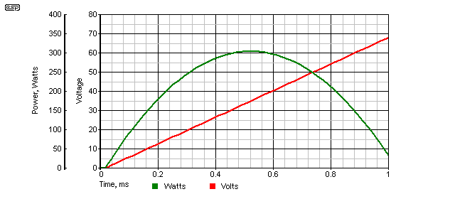
Figure 1 - Power Dissipation vs Voltage for Class-B Amplifiers
Figure 1 shows the dissipation of the output transistors of one side of a simple Class-B amplifier using a 70V supply and feeding a 4 ohm load. The dissipation is seen to increase until the output voltage reaches 35V (exactly half the supply voltage), after which it falls again. Only one side of the amplifier is shown, and the test circuit is seen in Figure 2. Naturally, in a real amplifier, the total average dissipation at any voltage is quite different with sinewave or music signals. This is covered later in the article. The average power dissipated for a continuous sawtooth waveform is about 204W.
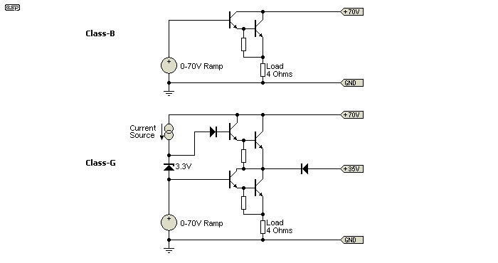
Figure 2 - Test Circuits for Power Dissipation
The test signal used was not a sinewave (or a half sinewave, to be exact), because that makes the power dissipation curve too complex for simple analysis. The linear increase of voltage shows the maximum dissipation very clearly, and it occurs at that point where the voltage across the load and output transistor are equal. For the test circuit, this occurs at 35V. With a sinewave signal, worst case transistor dissipation occurs when the RMS output voltage is roughly half the DC supply voltage - 35V RMS, or 306W into a 4 ohm load. Again, this only applies for a resistive load.
Two circuits are shown, Class-B and Class-G. These were used to capture the power dissipation waveforms, and to perform all power calculations.
Using the test circuit shown in Figure 2 and the same sawtooth waveform used for previous measurements, I measured load power and output device dissipation. For this exercise, driver transistor dissipation was ignored, as I deliberately 'fudged' the simulation parameters to keep this at a very low value (typically less than 1W). A 3-rail Class-G stage was also simulated, but is not shown. Ignoring losses, with 3 supplies, each at 23.33V, the inner devices naturally get 23.33V, the middle transistor supply is 44.66V and the outer devices 70V (close enough). Average dissipation is the sum of all power transistor dissipations (1, 2 or 3). Input power is the sum of the output power and the dissipated power in all output devices, and with a resistive load (this gives a slightly optimistic result). The results are tabulated below ...
| Measurement | Class-B | Class-G 2-Rail | Class-G 3-Rail | Class-G Switched Rail |
| Average Load Power | 381W | 381W | 381W | 381W |
| Average Dissipation | 204W | 151W | 133W | 143W |
| Peak Dissipation | 304W | 268W | 220W | 297W |
| Input Power | 585W | 532W | 514W | 524W |
| Efficiency | 65% | 72% | 74% | 72% |
The peak dissipation figures given are for the highest instantaneous power that is handled by the device(s). For Class-G, this is always the outermost devices, regardless of the number of supply rails. As is readily apparent, increasing the complexity to use three supply rails gives a marginal improvement in efficiency. Also, bear in mind that the overall efficiency of any Class-G amp is affected by the dynamic range of the programme material and the overall level. The above data show the dissipation and efficiency with an applied 0-70V sawtooth waveform, but this is a highly unlikely waveform in the real world. Also note that this is only one half of an amp, and is used for explanatory purposes only.
Actual results will vary - possibly widely - depending on the usage of the amplifier. One thing is obvious, and that's that a 3-rail system has a minimal improvement over two rail systems. The switched-rail variant is discussed below, but was included here to keep the data organised, and to allow easy comparison.

| It must be understood that the efficiency figures shown above are different from the generally published values. This is because a sawtooth waveform was used, and not a sinewave. Half sinewave testing will change the numbers, but the relationships will remain fairly similar. For the Class-B example, load power is 287W, transistor dissipation is 90W, and efficiency is 76%. Class-G improves this, with 71W dissipation and 80% efficiency. These figures are for full power, and are not representative of expected performance with music signals. |
This arrangement is popular because it's relatively simple to achieve, and if done properly gives very good results. The remainder of this article will concentrate on this topology, although there are others that can also be used. These will be discussed later, but not in great depth.
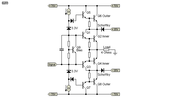
Figure 3 - Basic Principle of Class-G Amplifier
The output stage above will be used for all further analysis of the Class-G output stage. The front-end and VAS (voltage amplifier stage) are virtually identical to any normal Class-B amplifier. The VAS would normally be used in place of one of the current sources shown. The arrangement above is convenient for analysis because it is quite straightforward.
Because the inner transistors (Q2 and Q5) are supplied with ±35V, both inner output transistors and drivers must be rated for at least 105V breakdown voltage. The voltage across each will vary by the full inner supply voltage plus the difference between the inner and outer supplies of each polarity. As the output swings between positive and negative, the inner transistors will therefore get a maximum voltage of 70 + 35 = 105V, however prudence suggests that a higher rating is preferable, and ideally one would use transistors rated for the full supply voltage. Once the signal calls for a voltage exceeding 35V of either polarity, the outer transistors (Q6 and Q8) boost the supply voltage in the direction required, allowing the output voltage to swing by almost the full ±70V. Even a small miscalculation (in design or implementation) may cause large amounts of magic smoke to escape from expensive devices, and a great number of rude words to be uttered.
The voltage across the outer transistors can (in theory) never exceed 35V, so low voltage, high power transistors may be used. If higher voltage devices are used, their SOA (safe operating area) should be very good - depending on the devices chosen of course. A good SOA is necessary, because by the time Q6 (for example) turns on, it will be expected to supply 8.75A with the full 35V across it. This is an instantaneous power of 306W, far more than any one transistor can withstand without failure. At the point where Q6 turns on, Q2 (the inner transistor) is turned on fully, and remains so until Q6 turns off again. Consequently, the dissipation in Q2 and Q4 will remain quite low whenever the output voltage is greater than 35V in either direction.
With the supply voltages shown, the diodes providing the ±35V supplies must be rated for a continuous average current of at least 5A, preferably more. The voltage rating is not a problem, since the maximum reverse voltage is 35V with the supplies shown.
The main influences are ...
The power dissipation (using the same signal as used for Figure 1 and the Class-G circuit shown in Figure 2) is shown below. Whilst more complex because of the two sets of transistors, there doesn't appear to be a vast overall difference at first glance.
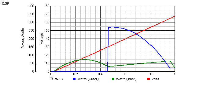
Figure 4 - Power Dissipation of Class-G Amplifier
To appreciate the effect, one must look at the area below the curves, and determine the average power. The outer supplies remain at ±70V in all cases. For the inner transistors with 35V supplies, the average power - using exactly the same waveform as used in Figure 1 (and looking only at a positive signal) - is about 40W, and for the outer transistors (Q6 and Q8) it's 100W. The total is therefore 140W vs 203W for Class-B, a significant reduction. The ratios will change with differing supply voltage distribution. The total power will rise to 158W if the inner supplies are reduced to 30V. Conversely, if the inner supplies are raised to 40V, the total average power is reduced slightly to 136W, and with inner supplies of 45V the total average power falls further to 129W.
It would seem logical that the inner supplies should therefore be around 70% of the total, and indeed, this will give the lowest overall dissipation - but only for continuous signals at full power. The real world is very different, and amplifiers are not usually operated at full power with a continuous waveform. They are used for music, and as discussed above, there are many factors that influence the optimum inner voltage.
Most professional power amps that use a dual voltage supply will aim for the low voltage supply to be between 40% and 50% of the main (high voltage) supply, but there can be significant variations. When used for hi-fi applications, the low voltage supply may be as little as 30% of the high voltage, since the amplifier will typically spend well over 90% of it's time without ever turning on the outer transistors. Different designers will have different opinions, but the end result will usually be fine for most purposes. The point is that there is no optimum percentage - there are too many variables.
There are several high power designs that use more than 4 supply rails (i.e. two positive and two negative voltages). There are some that have three supplies of each polarity, and even four is not unknown. As always, the law of diminishing returns applies, and the designer must balance complexity and cost against advantages. In most cases, this will result in a two or three stage output circuit (a total of 2 or 3 supplies of each polarity). The process for adding extra supplies is identical to that needed for a simple two stage Class-G stage, and multiple stages will not be examined any further.
As mentioned by Douglas Self [ 3 ], there is an additional topology that he refers to as 'shunt' Class-G. This is not too uncommon with some commercial amplifiers, but is not covered here. The primary difference between the series and shunt (or parallel) topologies is that the latter requires that the secondary output devices must be capable of withstanding the full voltage from the high voltage supplies.
The series connection only requires that the outer transistors be capable of the voltage difference between the two supply voltages. This can make the device selection easier, since only high power is needed, and not a combination of high power and high voltage. Safe operating area is also improved with the lower voltage.
|
| While the following is not normally publicised, it must be considered that certain test signals (in particular) may embarrass many Class-G amplifiers. Dissipation with some waveforms at specific levels may cause the amplifier to run far hotter than expected. This is not likely to be an issue with normal music signals, but it could still happen! For example, consider a signal to the amplifier that is clipped (due to incorrect levels set from the mixer or crossover perhaps), and just happens to push the amp to just above the commutation point (say 36V peak for our examples here). This is roughly the equivalent of a squarewave signal. Under these conditions, the amplifier output stage (Figure 3) will effectively be driven with a 36V squarewave signal. Power to the load is about 147W. A Class-B amp will dissipate ~150W, slightly less than may be expected. The Class-G amp will dissipate the same (150W), and this is the same as when delivering full power - under these conditions, Class-G has not reduced the dissipation at all! |
Efficiency Comparison
Because the efficiency at various powers and waveforms is so hard to quantify, the following graph will hopefully make it a little clearer. As you can see, the Class-G amp has higher efficiency (meaning lower losses and less heat output) over the full operating range. The two types of amp have the same maximum theoretical efficiency at full power. Note that the efficiency of Class-B and Class-G amps can approach 100% if they are driven into hard clipping, but this is not the way they are (or should) be used in practice.
The data are based on a sinewave signal and a 4 ohm resistive load. There is no correction for the power supply voltage collapsing under load - these are theoretical curves only, and are included to allow the difference to be seen easily. The circuit topology used for the graphs was based on those in Figure 2, but modified for bipolar operation. Correction for crossover distortion was included, since the Figure 2 circuits have no provision for transistor bias.
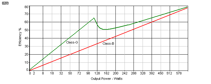
Figure 5 - Efficiency vs Output Power of Class-B and Class-G Amplifiers
The graph for Class-G looks decidedly odd, but this is real data. At an output power of about 100W, the Class-G amp peaks, and falls again as power is increased further. Minimum efficiency after the peak occurs at ~160W, after which it increases again. The graph was produced by analysing the average power into the load and from the power supply (or supplies), with the peak output voltage raised in increments of 1V. The dip after 100W is the point where the outer transistors start conducting - see Figure 4, and compare the effects of combining the two sets of dissipation data.
The reason that the Class-B graph is a straight line is because of the power scale which is based on equal increments of voltage so is not linear. Changing scales does not change the data of course, but this was the simplest way to obtain the graph, ensuring there were enough data points to get an accurate result. The important thing to notice is that Class-G is more efficient over the full normal working range of the amplifier, and especially so for material with a reasonably wide dynamic range.
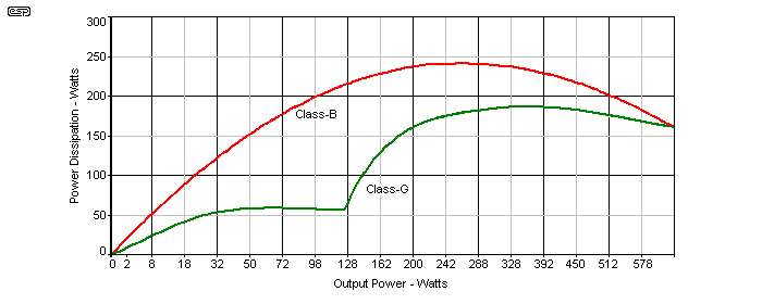
Figure 5A - Dissipation vs Output Power of Class-B and Class-G Amplifiers
Figure 5A is essentially the same data used for Figure 5, but applied differently. In this chart, the dissipation (via the transistors and heatsink) is plotted against output power. This gives an alternate way to view the difference in heat between Class-B and Class-G. As is quite apparent, the heat is reduced dramatically by using Class-G. The overall curve shape is similar to the sum of the two dissipation curves in Figure 4, but is modified because of a sinewave signal instead of a voltage ramp.
The simple Class-B and Class-G stages both showed a continuous average power into the load of 196W. No surprise, since both used the same signal. The Class-B stage had a transistor dissipation of 245W - this is a lot of heat to get rid of! By comparison, the Class-G stage showed an outer transistor dissipation of 87W, and an inner transistor dissipation of 48W - a total of 135W. This is just over half the dissipation - a significant reduction.
Peak dissipation is also improved considerably. The Class-B stage had a peak dissipation of 306W. This means that even 4 x 200W transistors may be pushed past their limits for each side of the amp (positive and negative, not left and right) - remember the SOA curves, temperature derating and dissipation with reactive loads.
By comparison, the Class-G stage showed peak powers of 269W (outer) and 72W (inner). While it is obvious that the outer sections will need at least 3 x 200W transistors, remember that they do not need to be high voltage. This reduces the financial burden. The inner transistors could use a single 200W transistor, which will be well within its ratings, even at elevated temperature and a reactive load. For ease of comparison, these figures are tabulated below. All figures are for a 4 ohm resistive load. Results into reactive loads (e.g. loudspeakers) will be very different, and are too difficult to predict. I've taken a few measurements, but all averages are based on estimates.
Expect the peak dissipation to double with a worst-case 45° phase shifted current as produced by a reactive loudspeaker load. This is no different from a Class-B amplifier, except that there is a much greater saving with Class-G. All output devices must be able to withstand the worst-case peak dissipation while remaining within their safe operating area at normal operating temperature - not 25°C. This is commonly overlooked by novices, most of whom will (often seriously) over-estimate the power they can get from any given semiconductor.
| Condition | Class-B | Class-G |
| Average Load Power | 196W | 196W |
| Peak Dissipation (outer) | - | 269W |
| Peak Dissipation (inner) | 306W | 72W |
| Average Dissipation (outer) | - | 87W |
| Average Dissipation (inner) | 245 | 48W |
| Average Dissipation (total) | 245W | 135W |
| Average Dissipation (total, reactive) | 320W | 180W |
Since a Class-B amplifier doesn't have two sets of devices, the Class-B figures have been included in the 'inner' categories. As you can see from the table, the difference is most worthwhile. Being able to use a heatsink that's less than half the normal size with an inexpensive fan means that a very powerful amplifier is easily made to fit into a 2U rack case (89mm or 3.5" high). Because of the lower losses, this also means that smaller transformers can be used.
Since a single channel Class-B amp will waste 245W (from the table) while providing 196W into the load, the transformer and power supply must supply 441W so the amp can do its job. The Class-G amplifier requires 331W to do exactly the same work in the load - a saving of 110W in total.
The saving is greater is you consider the reactive load dissipation, which as noted above is roughly double that for a resistive load. As seen in the table, this will be (typically) around 320W (or 490W for single frequency, 45° phase shift) for Class-B, but is manageable at 180W for Class-G. Attempting to calculate the real contribution of reactive loads is very difficult, because the signal will change from capacitive to inductive (both are reactive) to resistive depending on frequencies present at any given time. In terms of the average contribution of reactance, it is not unreasonable to assume that it will add somewhere between 10-30% to the resistive dissipation. Again, this will vary depending on usage, speaker design, type of music, etc. I used 30% for the table.
As discussed earlier, it is impossible to predict the optimum voltage for the inner rail, because the signal is effectively random. This also means that every efficiency figure that can be produced can only be for a specific set of circumstances. I have attempted to provide sufficient information to allow the reader to understand the processes involved, but no-one can predict how any Class-G amplifier will perform in the end users' application, unless that application involves a signal that can be repeated exactly (in all respects!). There are simply too many variables.
There is no actual changeover from the inner to the outer pair of transistors, but instead, the inner rails can be considered to be boosted as the output attempts to exceed the lower voltage. In theory, the inner transistors remain in control of the signal at all times, however in practice this point is moot. Figure 5 shows the output signal and the voltage at the inner rails - the boosted voltage.
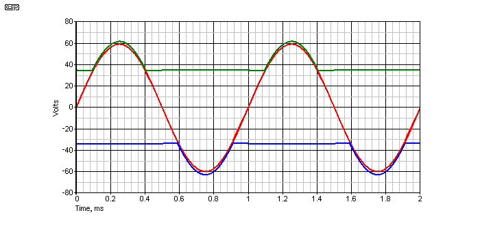
Figure 6 - Voltage Rail Boost Effect
As you can see, the rail voltage is maintained at a couple of volts above the output voltage. The outer transistors are really simply supply voltage boosters, and are designed to turn on just before the output clips at the inner rail voltage. Naturally, once the outer rail voltage is reached, the output will clip, since it can go no further. The switching process is commonly referred to as commutation, since the process is not hugely different from the operation of a brush commutator in an electric motor.
Commutation (or rail boosting) is accomplished using diodes and the outer transistors. As with any function that involves switching, distortion artifacts can be produced that will become part of the output signal, reducing sound quality. In this respect, it is similar to the crossover distortion that occurs when an amplifier fails to reverse its output polarity linearly.
Fortunately, the distortion occurs at a relatively high output level, and it is likely that any distortion will be completely inaudible. This is partly because of the low level of distortion compared to the output level, and partly due to masking, where sounds become inaudible when in the presence of other sounds of a similar frequency but higher levels. This phenomenon is exploited in all MP3 coded audio files, for example. While it is entirely possible that the distortion may be audible with a sinewave input, as the complexity of the music increases the audibility of the distortion reduces. The use of Schottky diodes for the inner rail voltages is highly recommended, as these switch off much faster due to a much lower stored charge, and are therefore less liable to generate audible artifacts.
The zener diodes shown in Figures 2 and 3 are essential. They ensure that the outer transistors start conducting just before the inner transistors saturate. At this point, the amplifier would normally clip, but the outer transistors now boost the supply rails to exactly the degree needed to prevent clipping. As noted elsewhere, once the output signal attempts to exceed the outer supply voltage (either polarity) the amplifier will (must) clip regardless. If the zener diodes are omitted, there will be considerable distortion generated at the commutation points. While negative feedback will reduce it to some degree, it will still be present, measurable and possibly audible.
If the zener voltage is too high, the outer transistors will turn on too early, which will increase the dissipation of the inner transistors. If too low, the outer transistors will not conduct early enough, and the output will have distortion at the commutation point because the inner transistors are no longer in control. Ideally, the zener voltage will be slightly higher than the voltage drop across the inner transistor circuits, including emitter resistors and the losses in the supply and outer transistor base diodes.
Like so many other areas of electronics, there is a balancing act (aka compromise) that must be made. In general, a zener voltage of between 3.3V and 4.7V seems reasonable for most applications, although some topologies will need more, others less.
Because the inner transistors work at relatively low voltages, it is much easier to provide excellent overload protection than would be the case for a high voltage Class-B amplifier. There is no need for a protection circuit that has multiple break-points (essential for Class-B high voltage designs), because the inner devices are usually easily contained within their safe operating area with a relatively simple circuit.
The protection scheme is simplified solely because of the low operating voltage for the inner transistors, and no other amplifier topology provides this inherent advantage. In the case of Class-G amps using three or more supplies of each polarity, the inner transistors only require protection for the lowest voltage rails.
Safe Operating Area
As an example, I have included the SOA data from the ON-Semi data sheet [ 5 ] for the MJL21193/4 transistors. These are rated at 200W, 250V and 16A continuous. They are rugged devices, and are well suited for high power amplifiers. The general trend is virtually identical for all bipolar transistors, although the numbers will change to match the device ratings.
As you can see, the voltage at maximum current is quite limited, but surprisingly, it extends slightly beyond the 12.5V limit imposed by the 200W rating. Still, it is well below the 35V limit for the outer transistors described here - at 35V, collector current is limited to around 7A. Remember, that is with a case temperature of 25°C. At higher temperatures, the transistor must be derated by 1.43W / °C. For example, with a case temperature of only 60°C, the transistor must be derated by 50W, reducing maximum dissipation to 150W.
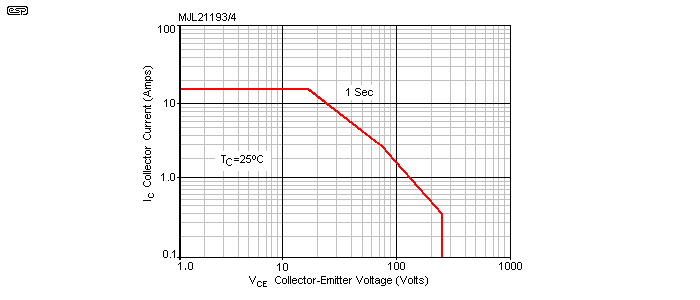
Figure 7 - Active Region Safe Operating Area
Quote from the data sheet ... There are two limitations on the power handling ability of a transistor; average junction temperature and secondary breakdown. Safe operating area curves indicate IC – VCE limits of the transistor that must be observed for reliable operation; i.e., the transistor must not be subjected to greater dissipation than the curves indicate. The data of Figure 7 is based on TJ (peak) = 200°C. TC is variable depending on conditions. At high case temperatures, thermal limitations will reduce the power than can be handled to values less than the limitations imposed by second breakdown.
For more information on transistor power dissipation, second breakdown and other limits, please see the SOA article.
One topology used by at least one manufacturer [ 4 ] is shunt or parallel mode, where the outer transistors actually do take over when the inner devices run out of voltage. Whether there is any real advantage is debatable, but of the designs I've seen it was done for a very specific purpose. The way these amps are configured allows the transistor collectors to be mounted directly to an earthed (grounded) heatsink. This minimises the thermal resistance between the transistor case and the heatsink, allowing the best possible device dissipation.
In my opinion, this is probably the most complex way to design a Class-G circuit, and I would not recommend even attempting it. Although the manufacturer does manage to make very reliable amps using this method, I am informed (by someone who has repaired them) that many of the components are highly critical - use a transistor even slightly different from the original, and the amp will suffer parasitic oscillation. For most of the semiconductors, it is stated on the schematic that they must be obtained from the manufacturer ... no substitutions of even the same brand of device.
I've been able to get several schematics for commercial designs, and the series configuration described here is still one of the more popular. As with many things in electronics, there will be as many alternatives as there are designers. Ultimately, it doesn't matter, provided the design has enough output devices to safely handle the worst case abuse to which the amplifier is liable to be subjected. For professional audio, this can amount to a great deal.
Yet another arrangement is to use a switched high voltage supply. The high voltage supply is switched on and off, rather than turn the supply on linearly to maintain 2-3V headroom over the signal. As soon as the threshold is reached (typically half the main supply), the full supply voltage is applied to the output devices, changing the supply voltage from (say) 35V to 70V in a single step. The full voltage remains across the output devices until the output voltage falls below the threshold, at which time the high voltage is turned off again. The output devices are then returned to the 35V supplies. Overall dissipation is potentially slightly lower than the series connection shown above, but commutation noise is almost guaranteed unless the switching is slowed to a reasonably leisurely rate.
With this arrangement, the inner transistors must handle the entire dissipation of the amplifier. Although average power is reduced compared to Class-B, the peak dissipation remains (more or less) the same - it just doesn't last as long for any given frequency. The greatest benefit is that switching MOSFETs can be used for commutation, and there is no need to use comparatively expensive audio power transistors. The rail supply voltage is shown in Figure 8, as a simple description is not sufficient to allow full understanding of the process involved.
There are undoubtedly other Class-G variants that I've not seen, and these may use other techniques.
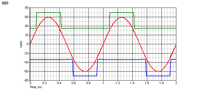
Figure 8 - Switched-Rail Class-G Supply Voltage
As noted above in the section about overall efficiency, this scheme has an equivalent efficiency to a conventional dual rail (each polarity) Class-G amplifier. Where it wins is in the outer transistors, which are now switching rather than linear. Consequently, the outer transistor losses are very small, but the peak dissipation of the inner transistors is now increased dramatically.
Because all amplifiers must be designed so that the output transistor safe operating area is not exceeded due to reactive loads or high operating temperature, the inner transistor power ratings must be the same as for a Class-B stage. Because average dissipation is lower, this helps to keep temperatures lower, and this can provide a small advantage. As with all Class-G schemes, the power transformer can also be slightly smaller, because of the lower overall losses.
A similar (at least in some respects) arrangement is called Class-H, and it can be difficult to decide exactly into which camp some amplifiers fall. Class-H is often described as using a 'bootstrap' capacitor that lifts the rails as needed, but cannot maintain them at the full voltage for more than a few cycles. After a short period, the capacitor discharges, and the high voltage supply collapses. Originally, there were used for car audio, and allowed much more power than can normally be expected (about 18W for a BTL (bridge-tied-load) amp operating from 13.8V DC). Being far cheaper than a switchmode power supply, this is a convenient way to get extra power for very little expense. A number of specialised ICs were/are produced for just this purpose.
Because the difference is rather blurred, you may see Class-G amps described as Class-H and vice versa. My preferred terminology is that amps that use a bootstrap circuit or an externally modulated power supply are 'real' Class-H. If the supply is switched or boosted using a separate fixed high voltage supply, then Class-G is the most appropriate description of their topology.
Hitachi is usually credited with the first Class-G amplifier, but from the descriptions I've seen, it actually appears to have been Class-H. The peak power of 400W into 8 ohms was not available continuously, but only for relatively brief periods. This implies that the high voltage rail was produced by bootstrapping a capacitor, rather than a switched rail design. By my definition above, that makes it Class-H, although Hitachi described it at the time (1978) as Class-G.
This level of confusion has never gone away, largely because only classes A, B, C and D are 'officially' recognised. As suggested in the introduction, you can feel free to use whichever term you prefer, because there is no standard.
The diagram below is not a project, and is intended only to show the general configuration of a Class-G amplifier. Both inner and outer transistors use separate drivers. This is one of a great many configurations that have been used, and in that respect can be considered as '"typical' as any other configuration.
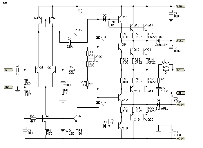
Figure 9 - Concept Schematic For Class-G Amplifier
The front end of the amp is quite conventional, and uses a long-tailed pair (Q1, Q2) coupled to a current mirror (Q4, Q5). The LTP is fed from a current source, using Q3. This drives the VAS (voltage amplifier stage, Q6), which is stabilised using a Miller capacitor. The VAS is also supplied using a current source, Q7. The bias servo (Q8) must mount on the main heatsink for the output devices. The driver transistors are connected in the Darlington configuration, because it is less prone to parasitic oscillation than the compound pair that I normally use. For high power amps, one of the most important factors is reliability and stability.
The output devices are shown as a parallel pair, for both inner and outer output transistors. Oddly enough, the outer transistors require more dissipation capability than the inner devices, primarily because of the peak power demands. The average dissipation will also be higher with some programme material, less for others. This is reflected in the choice of two parallel transistors for both the and outer inner devices, but three may be needed in practice.
The resistor values shown are for reference only, and are typical of those that may be used in a working amplifier. While the above circuit has been simulated pretty much exactly as shown, it has not been built and tested. It is a reference design, in that it allows the reader to gain an insight into the complete design. Should there be sufficient interest, a project may be developed for a Class-G amplifier, suitable for operation at the voltages indicated, or possibly a little higher.
As should be fairly obvious, it is not a trivial undertaking, nor would it be a cheap amplifier to build. Further complexity would be involved if the amp were to be rack mounted, since short-circuit protection is needed to be added as a minimum. As with most commercial Class-G amplifiers, a fan is essential for each heatsink unless oversize heatsinks are used. Fan(s) should preferably installed in such a way as to provide cooling for the power transformers as well as the heatsinks. All transistors from Q8 to Q20 need to be mounted on the heatsink. Smaller separate heatsinks must be used for Q6 and Q7.
Class-G amplifiers are not for the faint hearted, as will be apparent from the above. Because of relatively high voltages and considerable complexity, even a trivial mistake during construction can easily generate a cascade of exploding (expensive) parts. Now you all know why I have shied away from offering boards for anything more powerful or complex than the P68 subwoofer amp - it's already more than capable of providing the same power as the Class-G amp shown. Heat dissipation is higher, so it needs more heatsink for continuous operation - a reasonable compromise, since it's not intended in its basic form for continuous duty.
It would seem initially that Class-G can't hope to compete with Class-D (pulse width modulation amplifiers). The latter have a typical efficiency of around 85-90%, and even the best Class-G amp cannot match that. However, Class-D amplifiers are significantly more complex, and because of high frequency switching, PCB layout is critical. In addition, even with the best filter circuits available, there will be some RF (radio frequency) noise emitted. Most Class-D amplifiers also have a frequency response that is only flat for one load impedance. Since speakers are not resistive, the high frequency response can be a gamble.
Because of the potential for RF interference problems, Class-D amps may be avoided by many users. There is no doubt that Class-D amps can deliver excellent fidelity and very little heat even at high power levels, but this doesn't mean that they are universally accepted as the most ideal power amp where high power and almost infinite reliability are needed. Music tour operators also have to consider the life of the equipment, and it's not unknown for 20 year-old amplifiers to be in daily service. With (mostly) normal through-hole parts, little or no surface mount, and no highly specialised ICs, linear amps can be repaired even when 30 years old or more.
Class-D amps nearly all use surface mount devices (SMD), and specialised ICs are essential with most designs to obtain satisfactory performance. When these parts become obsolete, the amplifier must be thrown away - it can no longer be repaired if 'unobtanium' parts fail. Substitutes may exist, but will almost certainly have different pinouts, and perhaps a different SMD case style. This is becoming a real issue for many consumer products - they are increasingly becoming un-repairable, because of SMD and the short lifetime of many of the specialised ICs.
Professional products must stay clear of short lifetime parts whenever possible, because there is a huge difference between the expectations of retail consumers and tour operators and other pro-audio users. To make a pro product with an expected life of less than 10 years is asking for trouble. This includes the ability to service the gear, well past the point where a normal home consumer would have discarded the item for the latest model.
There have been a number of alternative schemes over the years, with possibly the best known being the Carver 'Magnetic Field Amplifier' [ 6 ]. This was a misnomer in most respects, but it used a TRIAC phase-cut circuit before the power transformer, which was much smaller than it would have been otherwise. As more power was demanded, the TRIAC turned on earlier, boosting the voltage and current available. The TRIAC circuit was (pretty much literally) a lamp dimmer on steroids, as the basic TRIAC trigger circuit used the same principle as a household lamp dimmer. The power amplifier used three supply rails, ±25V, ±50V and ±75V.
There is no doubt that the amp was innovative, produced prodigious power and needed little heatsinking for normal hi-fi usage. However, a continuous full-power test would cause the transformer to overheat and smoke fairly quickly. The amp was never designed to be able to produce full power on a continuous basis, so people who thought they could use it for high-power sound reinforcement applications quickly discovered the limitations. Although it's not stated, the Carver amp didn't increase the supply voltage under load, but regulated it using the TRIAC. The transformer was almost certainly wound with fewer turns than necessary, so with the TRIAC fully on the magnetising current would be much greater than normal. This only happened with high current output to accommodate transients or short but loud music passages.
Similar approaches have (apparently) been tried using switchmode power supplies, but I don't have any more information. A potential limitation is that a transient may not last long enough to boost the supply voltage, and may result in transient clipping. While there are ways that this could be overcome, they haven't been adopted as far as I'm aware.
Main Index
Articles Index