
|
|
| Elliott Sound Products | Bipolar Junction Transistor Parameters |
 Main Index
Articles Index
Main Index
Articles Index
There are many things about transistors that confuse the beginner and no-so-beginner alike. Some circuits are easy and don't require much more than Ohm's law, while others seem a great deal harder. Paradoxically, it's often the circuits that appear to be the simplest that cause the most problems. A perfect example is a BJT amplifier circuit, using only a single transistor and a pair of resistors (as shown in Figure 1). While this topology is easily beaten by even the most pedestrian opamp for most things, it offers a fairly easy way to determine the transistor's parameters. There are even applications where it's useful, particularly where there are no opamps in the circuit and you need a gain stage.
Only a few simple calculations are needed to let you determine the DC current gain (aka β / hFE), with the benefit that you can set the transistor's actual operating conditions when setting up the test. This is a useful tool to let you understand how the transistor functions, and is easily adapted to the task of matching devices if that's something you need to do. While most circuits don't need matched devices, in some cases doing so improves performance.
In the circuits shown below, the input coupling capacitor has been selected to give a low frequency -3dB frequency of around 10Hz. This is not part of the process for determining the DC characteristics, and is only necessary to measure AC performance. While it's not required, I expect that most readers will want to run AC tests, and they are informative (even if not actually very useful). If nothing else, an AC test that includes distortion measurements is useful to determine the overall linearity - a truly linear circuit contributes no distortion.
A transistor can be in one of three possible states, cut-off (little or no collector current flows), active (or 'linear') and saturated (collector voltage at the minimum possible). For amplification, we need to be in the active region. The cutoff and saturated regions are only of importance in switching circuits. In these cases, it's generally accepted that the base current should around 1/10 of the collector current, regardless of the transistor's β. That means that almost any transistor will work, provided it's rated for the current and voltage used in the circuit. While it's common to see questions asked about substitutions, if you know these basic facts you can work out for yourself what will (or will not) work.
Beta; β: This is the basic notation for the forward current gain of a transistor. hfe: This is the current gain for a transistor expressed as an h (hybrid) parameter. The letter 'f' indicates that it is a forward transfer characteristic, and the 'e' indicates it is for a common emitter configuration. The small letter 'h' indicates it is a small signal gain. hfe and small signal Beta are the same. hFE: The hFE parameter describes the DC or large signal steady state forward current gain. It is always less than hfe.
The terminology can be different, depending on what source material you're looking at. Not all agree that the terms as shown represent the characteristics, and hfe and hFE are often used interchangeably. Ultimately, the terminology doesn't matter all that much, provided you understand the concept of current gain. Transistors are essentially current-to-current converters, so a small base current controls a larger collector current. Emitter current is always equal to the sum of the base and collector currents.
Note: This article is not intended to show the way to build a simple transistor amplifier, but to allow you to determine the parameters of a transistor. The circuit shown in Figure 1 will definitely work as an amplifier, but it needs input and output capacitors, and it has a very low input impedance. As shown (and perhaps surprisingly), the input impedance is around 660Ω - much lower than you'd expect. This is due to the feedback provided by R2, which acts for both AC and DC. The DC feedback stabilises the operating conditions, and the AC feedback causes the input impedance to be reduced. If the transistor had infinite gain, the input impedance would be zero!
For the time being, we'll ignore the AC performance, and just examine the biasing requirements. The circuit is shown below, and it would appear to be fairly easy to analyse because it is so simple. However, looks are deceiving. It doesn't take much prior knowledge to determine that the Figure 1 circuit will be in the active region. You only need to look at the resistor values in the collector and base circuits. Since R2 is 240 times the value of R1, it follows that the base current will be in more-or-less the same ratio. If the transistor has a β of around 250 (not at all uncommon), the circuit should bias itself towards the centre of the supply range (i.e. somewhere between 5V and 7V).
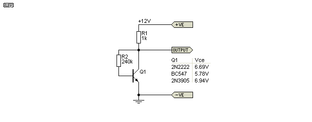
Figure 1 - Collector-Base Feedback Biasing
The analysis problem lies in the word 'feedback'. Whatever happens at the collector is reflected back to the base, so the collector voltage is dependent on the base current, which in turn is dependent on the ... collector voltage! The transistor's hFE changes the relationship between collector and base, and without knowing one of the parameters in advance, it's simply not possible to predict exactly what the circuit will do.
Will the collector voltage be at or near the supply voltage (cut off), ground (saturated), or somewhere in between (active)? The only thing we know for certain is that it will be somewhere in between the two extremes. Provided the transistor is functional (that much should be a given), it's not possible for the collector voltage to fall to zero, nor can it reach the supply voltage. In the first case, the base always needs some current for the transistor to conduct, and in the second case, if the transistor has base current, it must be drawing collector current. Therefore, there must always be some voltage (however small) across the collector resistor.
Even knowing the transistor's gain doesn't help a great deal, because the process is iterative. You'd need to make a guess at the collector voltage, and run a few calculations to see if that gave you a sensible answer, then adjust your guess up or down as appropriate until you arrive at a final figure. It's far easier to build (or simulate) the circuit than to try to second-guess a (somewhat non-linear) feedback network.
It's generally safe to assume that the collector voltage will be roughly half the supply voltage for a transistor circuit that is intended as a linear amplifier. There may be exceptions of course, and the actual collector voltage may be quite different from your first guess. Look at Figure 1 again, and assume a β of 240 for Q1 (based on the relationship between R1 and R2). That means its base current is 1/240 of the collector current. Since there's around 6V across R1 (collector resistor), the current must be around 6mA. That means that the base current can be estimated at 25µA. The voltage across R2 (collector to base) can be calculated using Ohm's law (but we'll ignore base-emitter voltage) ...
V = I × R = 25µA × 240k = 6V
If that were your first guess, you'd be very close! Your initial estimate may not be possible if you underestimate the gain, because we know that the voltage across R2 can be no more than Vce - Vbe (around 5.3V). For example, if your first guess at gain was 150, the voltage across R2 would be way too high (around 9.6V at 40µA). Unless you're after an accurate determination (which is neither needed nor useful), that's actually close enough! I know that it may not appear so at first, but consider that in production, transistors of the same basic type have a gain 'spread' that means no two transistors are guaranteed to give the exact same results. The base to emitter voltage also varies - it's typically taken to be 650mV (0.65V), but that depends on the specific transistor, base current and temperature.
The important thing is that great accuracy doesn't matter. If the circuit is designed properly (and it's actually hard to do it 'improperly' with this particular circuit topology), it will work as intended almost regardless of the transistor used. A circuit such as that shown should never be expected to have an AC output of more than around 500mV to 1V RMS, where its distortion should remain below 1%.
It may not be apparent that the circuit shown in Figure 1 can actually be extremely useful. It won't be as an amplifier though, but it allows you to match transistors very closely. The thing that needs to be determined first off is the expected collector current, and knowing the collector-base voltage that will apply in the circuit needing matched devices may also help. For example, a power amplifier may use ±35V supply rails, and the input stage may run with a total current of 4mA (set by the long-tailed-pair 'tail' current). However, you don't really need to provide the full collector-base voltage that will ultimately be used.
You now know that current through each transistor should be 2mA. A 20V supply will do just fine for most tests, and good results can still be obtained with a lower voltage. Based on the transistor datasheet, you can get a reasonable initial estimate of the hFE, and use a collector resistor that will drop about 2V at 2mA (1k). Then select an appropriate collector-base resistor, or cheat and use a 1MΩ resistor in series with a 1MΩ pot. The transistor should be installed into three receptacles of an IC socket, or use a solderless breadboard. For example, if the transistors you are using have an hFE of 200, then you know the resistor should be around 1.72MΩ.
Once you have a pot setting that drops 2V across the 1k resistor, the current is 2mA. Then just install transistors until you find a pair that have the same voltage drop across the collector resistance, and the same base-emitter voltage. There will inevitably be a small discrepancy because finding two that are identical is unlikely, but if they are within (say) 5% of each other then that's perfectly acceptable. When installed in the PCB, the two transistors should be thermally bonded, and that ensures that thermal changes affect both devices equally.
In a simulation with three different transistor types (2N2222, BC547 and 2N3904), the AC output voltage is 161mV, 170mV and 132mV (RMS) for an input of 1mV from a 50Ω source. The variation from the highest to lowest gain is only a fraction over 2dB, and these are very different devices. It's educational to look at their datasheets to see just how different they are, yet all work nearly as well as the other without changing the circuit. The 2N3904 has less gain, but the other two perform almost equally. The distortion is nothing to crow about, but that's expected of a high gain stage with no feedback.
Note that a single stage amplifier such as this is inverting, and it makes no difference if you use a valve (vacuum tube), BJT, JFET or MOSFET. When operated with the emitter, cathode or source grounded, all devices are inverting. A positive-going input causes a negative-going output and vice versa.
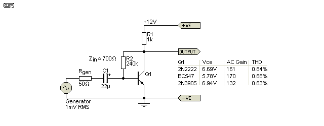
Figure 2 - Collector-Base Feedback Biasing (AC Measurements)
It's tempting to think that the AC gain of a transistor stage is determined by the DC current gain (β or hFE). This isn't the case at all, although the two are related. A transistor functions as a current-to-current converter, where a small current at the base controls a larger current in the collector (and emitter). While this does describe the actions that occur within the device itself, we tend to apply most of our efforts towards voltage amplifiers. However, one does not exist without the other.
For example, we can easily calculate that the β of the 2N3904 is around 200, yet if the collector is fed from a very high impedance we can obtain an AC voltage gain of over 3,300 quite easily. This technique is surprisingly common, and it's used in nearly all power amplifiers as the 'Class-A amplifier' (aka VAS - 'voltage amplifier') stage. The collector is supplied via a constant current source. This provides the desired current, but at an exceptionally high impedance. (An 'ideal' current source has an infinite output impedance.)
I stated above that the circuits shown here include feedback. It may not be immediately obvious, but R2 (collector to base) is a feedback resistor. The feedback is negative, so if the collector voltage attempts to rise, more base current is available (via R2) and the transistor is turned on a little harder, trying to keep the collector voltage stable. This feedback acts on both AC and DC signals, and the input impedance is very low. In fact, the input impedance with the circuit shown is less than 1k (ranging from around 650 to 750Ω), which makes it useful only for low impedance sources. This is one of many different reasons that the circuit shown is not common - very low input impedance, high distortion circuits aren't generally considered useful for most audio applications.
Not that this prevented it from being used back when transistors were expensive and were still in the process of being understood by most designers. However, even then, it was used only for 'non-demanding' applications where its limitations wouldn't be noticed. Today most people wouldn't bother, because there are opamps that are so cheap, flexible and accurate that it makes no sense to use an unpredictable circuit with so many limitations.
Just for the fun of it, I set up the above circuit, exactly as shown. The supply was 12V DC, and I used a number of transistors. Most were BC546 types (only 4 test results are shown), but from two different makers, and I also tested a few BC550C devices as well. I even tested a BC550C with emitter and collector reversed (after all, they are bipolar transistors). The measured results are shown in the table (I didn't measure distortion). The base-emitter voltage (Vbe) was around 680mV for the BC546 tests, but it wasn't measured for the BC550s.
| VCE (DC) | hFE (Calculated) | AC Output (RMS) | AC Gain |
| BC546 | |||
| 5.94 V | 276 | 1.52 V | 152 |
| 5.80 V | 291 | 1.52 V | 152 |
| 5.77 V | 293 | 1.52 V | 152 |
| 7.20 V | 177 | 1.24 V | 124 (-1.8 dB) |
| BC550C | |||
| 4.36 V | 498 | 2.04 V | 204 |
| 4.31 V | 508 | 2.04 V | 204 |
| 3.65 V | 675 | 2.12 V | 212 (+0.3 dB) |
| 4.83 V | 414 | 1.92 V | 192 (-0.5 dB) |
| BC550C Reversed! | |||
| 8.39 V | 112 | 255 mV | 25.5 |
The results are interesting. Quite obviously, when a low collector voltage is measured, the transistor has a high (DC) gain and vice versa. What is not so apparent is the reason for the variation of AC output voltage, with an input of 10mV RMS input from a 50Ω generator. Equally, several transistors show identical voltage gain, even when it's apparent that their hFE is different. You can expect the AC voltage gain to be related to the transistor's hFE, but there is obviously more involved.
Part of the reason is the intrinsic emitter resistance 're' (commonly known as 'little r e'), which is roughly 26/Ie (in milliamps). If the emitter current is 2.6mA then re is 10Ω. This is not a precise figure, but it's generally close enough for rough calculations. Because it changes with emitter current, it follows that the voltage gain also changes along with emitter current, so the gain is different for a positive input signal (which increases Ie) and a negative input voltage (which decreases Ie). The result is that re changes with signal level, causing distortion. It's also worth noting that a test with 'real' transistors and a simulation give answers that are surprisingly close.
Many early audio designs used comparatively high supply voltages to minimise the change of re by reducing the current variation for a given voltage output. Most of this was rendered un-necessary when more refined circuits with high open loop gain and negative feedback replaced simple transistor stages. These are covered in some detail in the article Opamp Alternatives.
The end result of all of this is that you can determine the parameters of a transistor by installing it in a circuit such as that shown here. You don't need a transistor tester, and the results you obtain will be as accurate as you'll ever need. This is basic circuit analysis, and it helps you to be able to understand more complex circuits, and to appreciate the value of basic maths functions. Mostly, you need little more than Ohm's law to work out the transistor's characteristics.
The main parameter (and the one that most people seem to be interested in) is DC current gain - hFE or β. You only need two voltage readings to be able to determine the gain (assuming that the supply voltage is fixed and a known value, such as 12V). Measure the voltage at the collector and base, with the common point being the emitter (this is a common-emitter stage after all). Now you have all you need to work out the gain.
First, determine the collector current, Ic. This is set by the voltage across R1, which is Vcc - Vce (assume Vcc to be 12V for this example). Then work out the collector current. I'll use a Vce of 6V, but it will rarely be exactly half the supply voltage.
Ic = ( Vcc - Vce ) / R1
Ic = ( 12 - 6 ) / 1k = 6mA
Now you measure the base voltage, and determine the current through R2 (240k). We'll assume 0.68V for the example. The current in R2 is the base current.
Ib = ( Vce - Vb ) / R2
Ib = ( 6 - 0.68 ) / 240k = 22.17µA
Gain is simply Ic / Ib, so is 6mA / 22.17µA, which comes to 270. That's the transistor's DC current gain. Yes, it is more tedious than reading it from a transistor tester, but it's the exact figure obtained in the circuit being tested. It will change with temperature and collector current, so it only applies in this particular instance. Ultimately though, the exact figure isn't particularly useful. It's not even really useful as a 'figure of merit', because the AC voltage gain of the circuit doesn't change a great deal even if hFE is different.
You can use a circuit such as this to match transistors as described in Section 2 if that's essential for the circuit you are building. Note that Vbe is still a variable, and that needs to be matched independently of hFE.
In most cases, a defined gain is required, and that's achieved with the addition of another resistor. In the drawing below, I added a 100Ω emitter resistor. The gain is now determined by the ratio of R1 to R3, plus re (internal base resistance). With 100Ω as shown, the theoretical gain is about 9.57 but it doesn't quite make it because the transistor has finite gain so the feedback cannot produce an accurate result. However, it's not too bad, and far more predictable than you would expect otherwise.
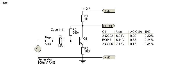
Figure 3 - Emitter Resistor Stabilises Gain
As you can see from the figures, ideally the circuits would have been re-biased to get a collector voltage close to 6.5V (there's a small voltage dropped across the emitter resistor). However, even with the same batch of very different transistors, the gain variation between the highest and lowest gain is now a mere 0.15dB. Distortion is also reduced, but not by the same ratio as the gain reduction. The addition of an emitter resistor is called emitter degeneration, and it is not the same thing as negative feedback. It's effective for stabilising the gain (for example), but does not reduce distortion as well as 'true' negative feedback. The noise from R3 is actually amplified by this circuit and all similar arrangements, so despite the reduction of gain, the noise will not be reduced in proportion.
Not immediately apparent is that the input impedance is much higher, being over 11k for each transistor simulated. The input impedance is (very roughly) determined by the emitter resistance (both internal and external) multiplied by the DC current gain. However, it's also affected by the negative feedback via R2, so it's not a straightforward calculation.
The gain is reduced further when an external load is added, because that is effectively in parallel with the collector resistor (R1). Output impedance is (almost) equal to the value of R1. It's actually a tiny bit less because of the negative feedback via R2 (about 990Ω as simulated). Emitter degeneration does not affect output impedance, unlike negative feedback which reduces it in proportion to the feedback ratio.
I measured the distortion both with and without the emitter resistor. At a signal level of only about 230mV without R3, distortion measured 2.5%. When R3 was included. the gain fell to 9, and even with 900mV of output the distortion was 'only' 0.25%. While this looks like a fairly dramatic improvement, consider that no opamp ever made has that much distortion at any output level. It's also worth noting that the simulator estimates the distortion surprisingly well - for the same conditions the simulator claimed around 0.24%, which is very close to the measured value.
The Early effect is named after its discoverer, James Early. It is caused by the variation in the effective width of the base in a BJT, due to a change of the applied base to collector voltage. Remember that in normal operation, the base-collector junction is reverse biased, so a greater reverse bias across this junction increases the collector–base depletion width. This decreases the width of the charge carrier portion of the base, and the gain of the transistor is increased.
The transistor's Early effect has some influence over the performance (for AC and DC). At a collector voltage of 5V, the gain is almost exactly 200 (as simulated, Ib=20µA), and that rises to 215 at 10V and at 50V it increases to 317. As you can see from the graph, the slope is quite linear. It follows that as the collector voltage changes, so does the effective hfe. Graphs are shown for three different base currents - 15µA, 20µA and 25µA (the circuit shown only the 20µA current source). The collector current below 2mA (with a collector voltage of less than 500mV) is not shown as it's irrelevant here. The AC waveform is not included in the test circuit or the graph. It's notable that even at a collector voltage of 500mV, the transistor is functioning normally.
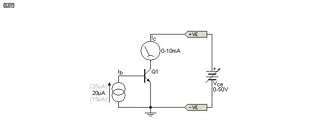
Figure 4 - Early Effect Test Circuit (2N2222)
There is also a change of re as the collector current varies, but I did not try to quantify that in the tests shown (it becomes relevant only when voltage gain is expected). No collector load resistor is used because the base current is maintained at a constant (and very low) value. Over the full range shown below, the AC gain changes by a factor of about 1.6:1 for the current range seen in Figure 5, and with a collector voltage between 1 and 50V. The AC voltage gain is almost directly proportional to the collector current. Although not shown in the test circuit or graph, the AC gain was measured. With a 1µA (peak) signal injected into the base, the AC current gain changes from a low of about 110 at 4mA collector current, to 165 at 6.5mA collector current. Voltage gain is not relevant to this test because only current is monitored.
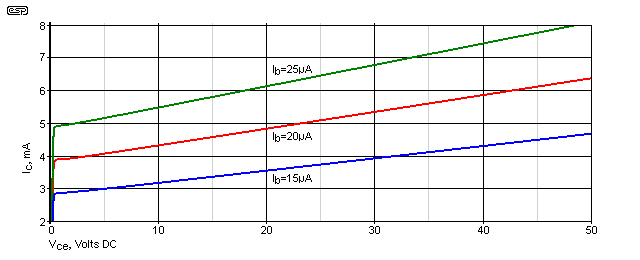
Figure 5 - Early Effect (2N2222)
While a look at Early Effect is an interesting observation, it's not especially useful for simple gain stages. In more complex circuits (especially linear ICs), it's common to keep the transistor's collector voltage as constant as possible. This can be seen in the input stage of most power amplifiers for example, where a significant amount of the complete circuit's gain is produced in the input stage. When a long-tailed-pair is used for the input, the collector voltage of the input transistors doesn't change by very much (if at all), so gain variations due to the collector-base voltage are minimised - but only when used in the inverting configuration.
This does not apply when an opamp is operated in non-inverting mode. Consequently, for a unity-gain amplifier, the collector to base voltage can vary from around 28V (peak negative input) down to as little as 2V (peak positive input). This voltage modulation can cause the gain of the input transistors to change by ±10% or more, due to the Early effect (although this is probably not the only reason for the increased distortion). Higher distortion in the non-inverting configuration is a well known phenomenon with opamps, although with competent devices any distortion that is added remains well below the threshold of audibility. Some devices have distortion so low that it's almost impossible to measure it, regardless of topology.
It's also worth noting that if a transistor is used for switching, you need to supply much more base current than you might think is sufficient. This is because at very low collector voltages, the current gain of a transistor is much lower than the datasheet figure. 'Common wisdom' is to ensure that the base current for a switching circuit is roughly 1/10th of the collector current, although you can often get away with less at low current. For the 2N2222 shown, if the switched collector current is 50mA you'd provide a base current of around 5mA to ensure that the 'on' state collector voltage is no more than 100mV. The datasheet claims that the saturation voltage (transistor fully on) is 300mV, with a collector current of 150mA and base current of 15mA. This indicates an hFE of only 10 to obtain full saturation. The datasheet only takes you so far, and you have to run your own tests to obtain realistic figures. It's essential to check a number of devices - a test based on a single transistor doesn't show you the likely results with different devices, even when they are all from the same batch.
It used to be that BJTs were the predominant technology for switching in digital systems (TTL - transistor-transistor logic). While CMOS (complementary metal oxide semiconductor) devices have now taken the lion's share in digital circuits, transistor switches remain very common. For high power we tend to think of MOSFETs as the most common switch, but IGBTs (insulated gate bipolar transistors) are now a better option for high voltage and high current applications.
Transistors used in switching applications don't operate in linear mode - that's for amplifiers. The transistor is either off (no collector current other than a tiny leakage current which can almost always be ignored), or it's fully on, in a condition known as saturation. The beta (or hFE) is only important to allow the designer to determine how much base current is necessary to force saturation. All switching systems will be subjected to higher than expected dissipation at the instant they are turned on or off. This is because the transitions are not instantaneous. Mostly, this isn't a concern, but it can become important if the switching signal (driving the transistor) has slow transitions. If too much time is spent in the active region (between 'on' and 'off'), peak dissipation can be much higher than expected.
Transistor switches are very common for turning on LEDs and relays, and for many other simple switching applications. NPN or PNP transistors can be used depending on the polarity, and many simple circuits rely heavily on BJTs as switches. There are few surprises, and the circuits are usually easy to calculate to get the appropriate base current to suit the load. The following circuit is common in projects from countless sources, and is also used to switch relays from microcontroller outputs (often only 3.3V at fairly low current).
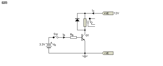
Figure 6 - Basic Switching Circuit
The load is shown as a relay, but it can just as easily be a DC fan, LED or a small incandescent lamp. We will know the supply voltage, and (usually) the load current. Using the relay example, if the coil measures 250Ω and it's rated for 12V, we can determine the current with Ohm's law (48mA). If we are using a microcontroller with 3.3V outputs, we only need to know the 'worst-case' gain (hFE) for the transistor to determine the value of Rb. If Q1 is a BC546, we can look at the datasheet and see that it can handle 65V (VCEO) at up to 100mA. The minimum hFE is 110, so to drive the relay, the base current should be at least twice the minimum allowed (most designers aim for between 5 and 10 times the calculated base current). With a 48mA load, base current will not exceed 436µA, so we'll allow 2mA. This is a little under the ×5 suggested, but it's still quite ok.
Because the base-emitter voltage will be 0.7V and we have a 3.3V base 'supply' voltage from the micro, Ohm's law tells us that the value of Rb must be 1.3k (2.6V at 2mA). We would use the closest standard value of 1.2k (or 1k) for convenience. This simple exercise demonstrates how easy it is to determine the values required for 100% reliable operation. Any other switching application is just as simple.
One of the interesting things about simple transistor switches (as opposed to Darlington or Sziklai pairs) is that the collector-emitter voltage will fall to only a few millivolts. You may expect that the collector voltage would be based on the base-emitter voltage, but it's not. With the values described, VCE will be about 110mV, but with more base current it falls further. Even as shown, the power dissipated in Q1 is only 5.28mW, which is negligible.
This won't always be the case of course, because the transistor has a finite switching time, and the worst-case is when it's 'half-on' (i.e. collector voltage of 6V as it goes high or low). In the circuit shown, there will be 24mA load with 6V collector voltage, so peak dissipation is 144mW. This is very comfortably less than the maximum continuous dissipation (500mW), and we don't need to change anything. The 144mW is a transient condition, and will typically last for less than 100µs if the input switches quickly enough.
Exactly the same set of simple calculations can be used for any transistor switching circuit. These circuits are very easy to design, but all of the steps need to be followed to guarantee reliability. If the relay were to be replaced with a fan drawing 200mA, the data sheet tells us that a BC546 can't be used (100mA maximum), and the selected transistor will need more base current. A BC639 can handle the current and worst case power dissipation. However, the minimum gain (as per the datasheet) is only 40, so you'd need at least 5mA base current, but preferably 10mA. This may be more than the microcontroller (or other source) can supply, and I leave it as an exercise for the reader to work out a way to achieve the desired results.
Remember that for switching, you need to supply at least twice the expected base current, and it's common to provide up to ten times as much to force full saturation of the transistor switch. BJT switching circuits become less attractive with very high current, because the base current is effectively 'wasted'. It doesn't contribute to the load current, and is simply another part of the circuit that has to be powered by the supply. Using a Darlington transistor is (or used to be) common, because the hFE is very high (up to 1k), so far less base current is required for saturation. However, a Darlington can't reduce its collector voltage to below 700mV, and at high current it may be as much as 3V.
For example, a TIP141 is rated for a collector current of 10A, and a gain of 1,000 at 5A. The saturation voltage with 5A collector current and 10mA base current is 2V, so it will dissipate 10W, even when driven into saturation. This is wasted power that has to be provided by the supply, but cannot be used by the load. Switching times are also rather slow, so high speed operation isn't recommended. The transistor must be mounted on a heatsink to maintain a safe operating temperature.
This is one of many reasons that MOSFETs are preferred for high current switching. A modern MOSFET may have an on resistance (RDS-on) of perhaps 40mΩ, and with a 5A load the voltage across the device will be only 200mV, dissipating 1W. The gate current is zero in steady-state conditions, but needs to be fairly high during switching (up to 2A or so, depending on the switching speed). However, this high current only lasts for a very short period, typically well below 100µs. Peak dissipation (during switching) may be up to 15W with the circuit described, but the average will be less than 600mW. Compare this with 10W dissipation for a Darlington transistor, and it's easy to see why MOSFETs have become the #1 choice for switching. With such a low total dissipation, a small section of PCB plane will usually suffice as a heatsink!
The main point here is to demonstrate the fundamentals of very basic transistor biasing, and to discover just how much one can learn from some simple observations. While I strongly recommend building and testing it, I recommend against using if for anything. It can be used for matching, but the main goal is to learn how a transistor works in a circuit. The actual topology doesn't matter as far as the transistor is concerned. It can only perform the one task - convert a small base current into a much larger collector current. By building it, you learn what it does at the most fundamental level.
It's also instructive to look at the AC performance. In particular, note that emitter degeneration (aka 'local feedback') is not as effective to reduce distortion compared to 'true' negative feedback. While the two tests shown indicate that the AC gain is reduced by a factor of around 17 (voltage gain reduced from 160 to 9.3), distortion is reduced by a factor of less than 6. With negative feedback, the improvement is roughly proportional to the reduction of open loop gain. Of equal importance, negative feedback also reduces noise, while emitter degeneration often makes it worse.
Not included in any of the above is any attempt to quantify the power supply rejection ratio (PSRR) of the circuits. This is a measure of how well the circuit can attenuate power supply noise, ripple, etc. It wasn't included for one simple reason - it's so poor that it means that a regulated (or very well smoothed) supply is essential. The power rail voltage must be completely free of any noise, because a full 50% of all supply noise ends up at the output.
Transistors are much more linear than generally believed if the collector voltage and/or current are not varied. This isn't possible in a real circuit, but most power amplifier and opamp input stages operate with an almost constant voltage and only the current is changed. The situation changes in the Class-A amplifier stage (aka VAS - voltage amplifier stage), but that is always operated with (close to) a constant current, and this time only the voltage varies. Most power amplifier and opamp input stages contribute a significant amount of gain, and operate with only small (often negligible) voltage changes due to the signal, and very small current changes as well. When forced to operate over a wide voltage range, the common mode input voltage changes significantly, leading to higher distortion (common mode distortion).
Running tests such as those described here is essential, not only for your own understanding, but to ensure that results will be consistent if a circuit is to be built by others (as a project perhaps). For example, all of the projects published on the ESP website take the normal variations of transistors into account. Because we know that no two components will ever be identical, a designer must consider the typical parameter spread of parts obtained by constructors. If this were not the case, many of the ESP projects would not work!
Note that cries of "I knew it - JFETs (or valves/ vacuum tubes) sound better!" are misplaced, because their distortion is generally higher than BJTs and there are different non-linear effects involved. There is no doubt that JFETs (and to a lesser extent IMO, valves) have their place in circuit design (including within opamps), but 'superior' sound quality is not amongst their virtues. This isn't to say that JFET input opamps sound 'bad' by any stretch - there are several such opamps that have excellent specifications (and sound quality). Every amplifying device known is non-linear, and only the causes (and remedies) are different. The use of valves in very low distortion circuitry generally provides performance that doesn't even come close to a decent opamp.
Switching circuits remain very common, and for low current operation a BJT is hard to beat. Base current is low, and it can be sourced from a low voltage. If you have more than ~1.5V available, it's easy to build a reliable switch that can handle up to 100mA easily. The design process is simple, and the result is usually very reliable if the design is optimised. They are also both readily available and cheap, two factors that are usually desirable (especially for high-volume production). In most cases, substitution is easy if the original part is obscure or out of production.
This article was inspired in part by Harry Powell (Associate Professor and Associate Chair for Undergraduate Programs) from UVA (University of Virginia), and is based (in part) on a 'Fundamentals 2' lab in Electrical and Computer Engineering. The original is entitled 'ECE 2660 Labs for Module 6'. The material forwarded was due to Harry seeing the article describing a Constant Collector Current hFE Tester for Transistors - Project 177.
There are no other references, because the techniques shown are quite common, and the data presented were the results of simulations and workbench experiments to verify results.
Main Index
Articles Index