
|
|
| Elliott Sound Products | Project 88 |

 Main Index
Projects Index Main Index
Projects Index
|
 Please Note: PCBs are available for this project. Click here for details.
The original preamp (Project 02) shown on these project pages is basically a good design, but in the interests of improved quality and reduced 'frills' this new version will fill or exceed most expectations. The quality comes largely from the use of good quality opamps, such as the Signetics NE5534 or Texas Instruments/ Burr Brown OPA2134. You can also use the LM4562 or other high quality opamp if preferred. If you use the NE5532, you may find that the small DC offset voltage at the outputs causes some potentiometer noise. If this occurs, use 10µF electros in series with the connections to the balance and volume pots. The polarity is not important, because there will less than 20mV DC across the caps, and polarised electros will last (almost) forever with such a low voltage.
Although they are conventional voltage feedback devices, modern opamps have few peers for sound quality, and I decided that it was time to make a PCB available. Capacitors in the audio path have been reduced to the minimum, and for those who want to, polypropylene caps can be used instead of the polyester types specified. Because of the very small PCB, these must mount off-board, but this will present few difficulties. I must point out that you will not hear any audible difference between polyester and polypropylene in a properly conducted double-blind test, despite what you may read elsewhere.
The key to this design is flexibility and simplicity, and the PCB has been designed with these primary considerations in mind. There is almost no configuration that is not possible, including adding tone controls if you wanted to use them. For even greater flexibility, you could even use two PCBs, although this will rarely be needed in practice.
There is much to recommend using pots on the inputs for CD and Tuner in particular, so their levels can be matched to the other signal sources you have. Although this option is not shown here, it is described in Project 02, and the pots would be used in exactly the same way as shown in the original hi-fi preamp schematics.
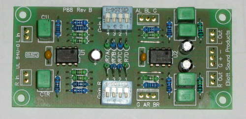
A photo of a completed PCB is shown below, as well as some specifications from my prototype.
The circuit is simplicity itself. Use of the PCB naturally makes it extremely easy to assemble, and this project may be combined with the RIAA (phono) preamp shown in Project 06 and the preamp power supply (Project 05) for a complete high fidelity preamplifier.
As shown, the maximum gain through the unit is 9dB (2.8 times), and this is in keeping with many of the latest offerings. More or less gain is readily available, simply by changing a 4-pole DIP switch. Use a 2 pole 6 position selector switch for your inputs, and you will have a preamp with enough inputs for everything.
Figure 1 shows the input selector, and the optional tape outputs. I recommend that the selector switch be located at the back of the preamp, close to the inputs. This minimises the chance of crosstalk or high frequency loss due to cable capacitance, and also limits the amount of shielded cable needed - not that it is expensive, but it is a pain to have to run 12 or 14 shielded wires from the rear of a preamp to the front panel where the switch is normally mounted. ESP was able to supply suitable extension shafts to extend the rather miserly 50mm or so that is usually provided with rotary selector switches, but these are no longer available (sorry).
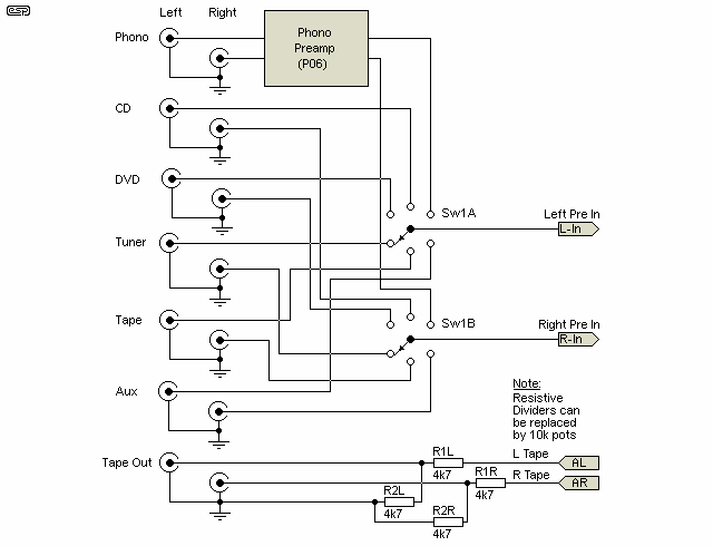
The 4.7k resistors (R1 L+R and R2 L+R) in each channel are used to bring the tape signal level back where it belongs, since there is 6dB of gain in the first stage. These resistors buffer the signal you are listening to from any possible degradation caused by the loading of the tape machine, and also ensure that the level to tape is exactly the same as the original. These resistors are not mounted on the board, but are easily accommodated on the tape out connectors. Naturally, there is no requirement to use them, and if you don't use tape, they may be omitted altogether.
The tape output can be made variable so that the level can be fixed at the best for a given tape machine. Simply use a 10k pot (preferably linear) to set the levels. There's also a change on the PCB, which requires that R5 (L+R) is replaced by a link, and the 1.5k resistor is moved 'off-board'. This prevents the balance control from affecting the tape out level, and also eliminates any small level change when you switch between the 'normal' and 'tape monitor' positions (see Fig. 3A).
Note: If first stage gain is set to 0dB as described below, then R1 (L+R) should be replaced with a 100Ω resistor, and R2 (L+R) omitted (the tape in and out connections are [almost] straight through).
The first amplifier stage uses one half of an OPA2134 opamp, with a gain of 6dB. With the values shown, response is -3dB at 3.4Hz, and is less than 0.5dB down at 10Hz. Input impedance is 100k - a little higher than the 'industry standard' 47k. The output of this stage then goes to the balance and volume controls. Again, these are not mounted on the PCB, since that would restrict you to the same type of pot and the same spacings as I used - this is too much of a limitation (IMO).
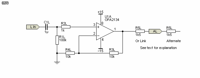
Earlier boards included RF interference suppression by adding a small capacitor between the two inputs of U1 (the space for this cap can be seen in the PCB photo, which is of an early board). This has now been removed, as it caused more problems than it solved - in particular, opamp oscillation with some devices.
The 'alternate' connection for R5 is useful if you include the tape monitor switch. By making R5 external, the 'AL' (and 'AR') positions are a direct connection to the opamp's outputs, ensuring that operating the 'tape monitor' switch doesn't cause any level change. It's no imposition as it's just two resistors that are relocated. The R5 position on the PCB is replaced by a link or a 10Ω resistor.
Although shown with 10k resistors for gain, you can reduce these for lower noise if you prefer. With the suggested OPA2134 (or NE5532) opamps, these resistors can be as low as 1k. The opamp input resistor (R2 L+R) can also be reduced in value, but at the possible expense of lower RF interference immunity. I wouldn't recommend less than 220Ω. The nominal options are for a gain of 0dB or 6dB, but you can get an intermediate gain of ~3dB by making R4 27k. This gives a gain of a bit under 3dB (2.74dB or ×1.37), which may be useful. You can change the gain easily by changing the value of R4 ...
Gain = ( 10k / R4 ) + 1 For example ...
Gain = ( 10k / 27k ) + 1 = 1.37
dB = 20 × log( Gain )
dB = 2.737
The points marked AL and BL are the same as in Figures 1 and 3, and refer to the Left channel only. The Right channel is identical, and uses the second half of the opamp (the Right channel uses connection points AR and BR - not shown in the drawings). Figure 3 shows the balance and volume controls. I strongly suggest that the balance control be retained, as I know from personal experience that it is a pain not to have the ability to centre the acoustic image properly. Moving speakers and furniture about is not always practical, and has an extremely low SAF (spousal acceptance factor). If you don't want to use the balance pot, it may be left out of the circuit entirely, and R5 (L+R) replaced with links or 10Ω resistors.
The volume and balance controls as shown use linear pots. These generally have better tracking than log pots, and the law of the pots is changed to be logarithmic by virtue of the added resistors. The balance pot will have virtually no effect on sound quality, since it is not in the signal path (it just forms part of a simple divider network). The relative impedances of the two networks are separated by a factor of 10, so interaction is extremely low.
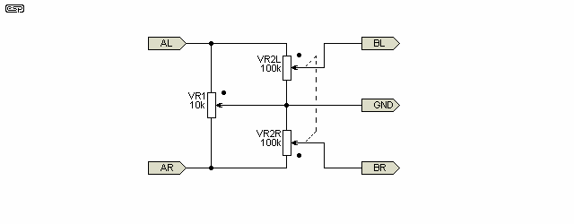
There is a loss of 3dB in the balance control, which means that if the balance is set to full Left (or Right), the system power will remain about the same, since the selected channel is boosted in power. In reality, there will always be an audible difference (apart from the missing channel), but maximum L-R balance settings will normally only ever be used for testing. The balance control has a wide central region, and this makes accurate setting of the system balance very easy - it is not at all 'touchy', where a small change in pot position causes a large change in relative levels, but is deliberately quite the reverse.
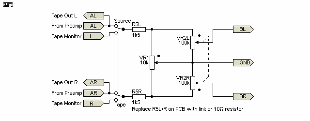
Since there seems to be something of a resurgence of tape machines, some constructors may wish to add a tape monitor switch. Figure 3A shows how it's done. The 'Tape Out' connections for each channel are connected as shown in Figure 1, and the tape monitor connections are returned to the preamp as shown above. Most tape machines have plenty of output level, so not having the first gain stage for tape monitoring should not cause problems. Naturally, this is only useful if you have a 3-head tape machine. Note that R5 (L+R) are mounted off-board, and their positions on the PCB are joined with links (or 10Ω resistors).
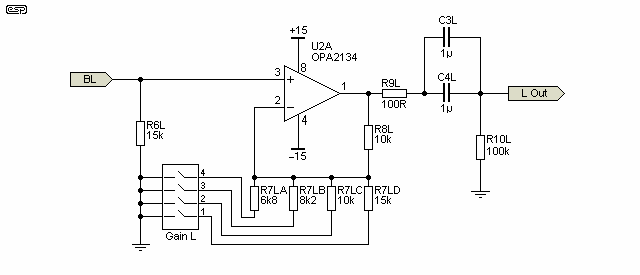
The second gain stage is similar to the first, with the main differences being the switched gain and output capacitors. The paralleled caps at the output are designed to ensure that the preamp can drive a power amp impedance as low as 22k with an overall response that is about 1dB down at 10Hz. If the preamp is being used to drive an electronic crossover or power amps that already have an input cap, then the output caps may be omitted and replaced with a wire link.
If you need more gain than this circuit provides as shown, you can use the table below to select a value for R7 (which is selectable using the DIP switch), leaving R8 as 10k in each case. I suggest that only the second stage gain be modified, to prevent the possibility of overload (distortion) of the first stage. As designed, there is no likelihood of any normal line signal distorting the first stage, and it can safely accept an input signal at just under 5V RMS without clipping. This gives the best signal to noise ratio - noise can be expected to be a little higher if the first stage has no gain. Even so, it is doubtful that noise will be audible with any system, provided low noise opamps are used.
| Stage 1 (dB) | Controls (dB) | Stage 2 (dB) | R7 (k Ω) | Tot. Gain (dB) | Sens (Ref 1V) |
| 0 | -3 | 6.02 | 15 | 1.42 | 850 mV |
| 0 | -3 | 6.93 | 10 | 3.00 | 707 mV |
| 0 | -3 | 7.86 | 8.2 | 3.91 | 638 mV |
| 0 | -3 | 8.90 | 6.8 | 4.85 | 572 mV |
|
| |||||
| 6 | -3 | 6.02 | 15 | 7.44 | 425 mV |
| 6 | -3 | 6.93 | 10 | 9.02 | 354 mV |
| 6 | -3 | 7.86 | 8.2 | 9.94 | 318 mV |
| 6 | -3 | 8.90 | 6.8 | 10.87 | 286 mV |
Stage 1 can have a gain of 0 or 6dB (voltage gain of 1 or 2, respectively). As shown, gain is 6dB, and to reduce it to 0dB replace R3 with a link, and leave out R4 in each channel. The table shows the different gains available from the entire preamp (with volume at maximum) for various values of R7 in each channel, and with Stage 1 having 0 and 6dB of gain. Generally, it will be quite rare that you need more than 10dB of gain in a preamp. The sensitivity referred to 1V means that this is the input voltage needed for 1V RMS output, with the volume at maximum. With all switches closed, the second stage has a gain of 5.36 (14.6dB), far more than anyone is likely to need. Intermediate gain can be obtained by closing more than one switch (I leave this to the constructor).
Operating the second stage with no gain is not recommended. It may oscillate due to the extraordinarily wide bandwidth of the opamps used, and the comparatively high capacitance at the inverting input. Having said that, it's only a few pF, and when operated with any gain there's little chance of instability. 0dB gain for the second stage is unlikely to be a requirement in practice.
For example, with a power amplifier having a typical sensitivity of 1.0V RMS for full power, a preamp gain of 10dB means that 320mV input will produce maximum output power with the volume at maximum. Higher level signals will require that the volume is reduced to prevent power amplifier clipping.
Because the preamplifier stages have gain to DC (there is no DC blocking capacitor in the feedback path), it is very important that any DC offsets do not get to the power amplifier - this is the reason for the 2µF of capacitance at the output of the preamp.
The PCB version is slightly different from that shown above, and uses either DIP switches or 0.1" jumpers to configure the gain. Full details are available when you purchase the board for this project.
The layout in Figure 5 is one possible way to build the preamp. Because it is powered from a wall transformer, the power switch needs only to be a low voltage type. This method of construction is very safe, and also keeps potentially noisy transformers well away from the preamp, thus ensuring that the noise level is as low as possible.
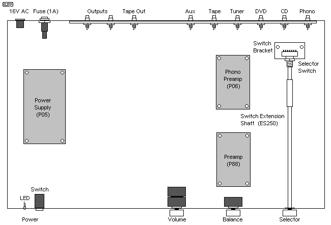
As shown, the preamp has a power supply board, one phono preamp and the P88 preamp PCB. The details of construction are left to the builder, since cases (etc.) will dictate to some degree the final arrangement of the various sections. The general layout shown keeps wiring to an acceptable minimum, and should ensure a very quiet preamp with absolutely top-notch specifications. The wiring has not been shown, but would follow the schematics shown above. I included a second output in parallel with the main output for convenience. If you don't need it, just leave it out.
For maximum shielding, the case should be all metal, but if a timber case is desired, aluminium foil lining will give very good results. The foil can be stuck down with spray adhesive. Make sure that a good earth connection is made to the foil, and any joins must have a screw to make sure that electrical continuity is maintained.
The quality of the parts used in this project is entirely up to the constructor. If you use high quality parts throughout, performance will rival many of the best preamps available. 1% metal film resistors should be used for all resistor locations, and the opamps must be bypassed using 100nF ceramic caps. Capacitors in the signal path are all polyester, and should be rated at 63V or better. Electrolytic supply caps are all 35V minimum rating.
The rest is up to you. Enjoy 
Having build a prototype of the board, I am able to give you some measured specifications, as well as the photograph of a completed PCB.
Measurements on this preamp were difficult - mainly because noise and distortion are too low to measure accurately. I haven't even tried to measure the distortion, but the figures I do have are as follows ...
| Parameter | Measurement |
| Frequency Response | 10 Hz to 250 kHz -0.4 dB |
| Noise | < 0.5 mV RMS at full gain (input open) |
| Crosstalk | Better than -58 dB at 100 kHz |
These figures were taken with the unit sitting on my workbench, in close proximity to fluorescent lights and with no shielding. Once mounted in a case with proper wiring (instead of clip leads!) noise and crosstalk in particular will be better than indicated. Crosstalk was measured at 100kHz, because I could not get an accurate reading at lower frequencies. Most was the direct result of input coupling - shorting the unused input gave a reading too low to measure.
I used 680nF (0.68µF) input and output caps, because I had run out of 1µF 63V units - 1µF/100V MKT caps are too big to fit in the space allowed. Even so, low frequency response is perfectly acceptable as indicated above. A -3dB frequency of 2.3Hz is adequate for all normal listening pursuits  . If preferred, you can use a 10µF electrolytic, which can be polarised or bipolar. There's no DC voltage to speak of, and even polarised electros will have a long and happy life.
| Main Index
Projects Index
|