
|
|
| Elliott Sound Products | AN-008 |
 Main Index
App. Notes Index
Main Index
App. Notes Index
Zener diodes are very common for basic voltage regulation tasks. They are used as discrete components, and also within ICs that require a reference voltage. Zener diodes (also sometimes called voltage reference diodes) act like a normal silicon diode in the forward direction, but are designed to break down at a specific voltage when subjected to a reverse voltage.
All diodes will do this, but usually at voltages that are unpredictable and much too high for normal voltage regulation tasks. There are two different effects that are used in Zener diodes ...
Below around 5.5 Volts, the zener effect is predominant, with avalanche breakdown the primary effect at voltages of 8V or more. While I have no intention to go into specific details, there is a great deal of information on the Net (See References) for those who want to know more. Because the two effects have opposite thermal characteristics, zener diodes at close to 6V usually have very stable performance with respect to temperature because the positive and negative temperature coefficients cancel.
Very high thermal stability can be obtained by using a zener in series with a normal diode. There are no hard and fast rules here, and it normally requires device selection to get the combination to be as stable as possible. A zener of around 7-8V can be selected to work with a diode to cancel the temperature drift. Needless to say, the diode and zener junctions need to be in intimate thermal contact, or temperature cancellation will not be a success.
The zener diode is a unique semiconductor device, and it fulfils many different needs unlike any other component. A similar device (which is in fact a specialised zener itself) is the TVS (transient voltage suppressor) diode. There are several alternatives to TVS diodes though, unlike zeners. Precision voltage reference ICs may be thought of as being similar to zeners, but they aren't - they are ICs that use a bandgap reference (typically around 1.25V). These are ICs, containing many internal parts. A zener diode is a single part, with a single P-N junction.
For reasons that I don't understand, there is almost no information on the Net on exactly how to use a zener diode. Contrary to what one might expect, there are limitations on the correct usage, and if these are not observed, the performance will be much worse than expected. Figure 1 shows the standard characteristics of a zener, but as with almost all such diagrams omits important information.
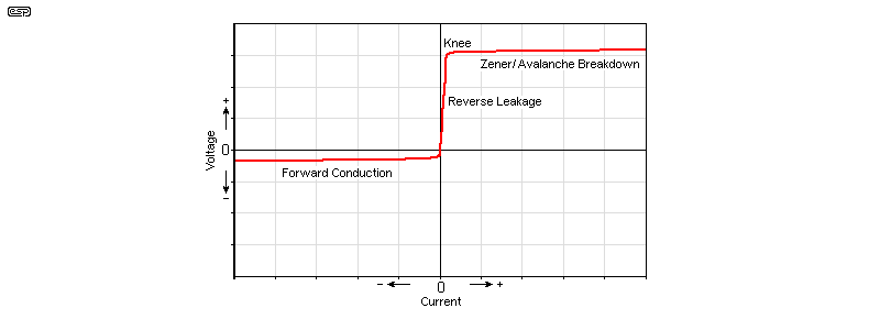
Figure 1 - Zener Diode Conduction
So, what's missing? The important part that is easily missed is that the slope of the breakdown section is not a straight line. Zeners have what is called 'dynamic resistance' (or impedance), and this is something that should be considered when designing a circuit using a zener diode. Standard (rectifier) diodes are no different, except that their dynamic resistance is important when they are forward biased.
The actual voltage where breakdown starts is called the knee of the curve, and in this region the voltage is quite unstable. It varies quite dramatically with small current changes, so it is important that the zener is operated above the knee, where the slope is most linear.
Some data sheets will give the figure for dynamic resistance, and this is usually specified at around 0.25 of the maximum rated current. Dynamic resistance can be as low as a couple of ohms at that current, with zener voltages around 5 - 6V giving the best result. Note that this coincides with the best thermal performance as well.
This is all well and good, but what is dynamic resistance? It is simply the 'apparent' resistance that can be measured by changing the current. This is best explained with an example. Let's assume that the dynamic resistance is quoted as 10 ohms for a particular zener diode. If we vary the current by 10mA, the voltage across the zener will change by ...
V = R × I = 10Ω × 10mA = 0.1V (or 100mV)
So the voltage across the zener will change by 100mV for a 10mA change in current. While that may not seem like much with a 15V zener for example, it still represents a significant error. For this reason, it is common to feed zeners in regulator circuits from a constant current source, or via a resistor from the regulated output. This minimises the current variation and improves regulation.
Manufacturers' data sheets will often specify the dynamic resistance at both the knee and at a specified current. It is worth noting that while the dynamic resistance of a zener may be as low as 2-15 ohms at 25% of maximum current (depending on voltage and power ratings), it can be well over 500 ohms at the knee, just as the zener starts to break down. The actual figures vary with breakdown voltage, with high voltage zeners having very much higher dynamic resistance (at all parts of the breakdown curve) than low voltage units. Likewise, higher power parts will have a lower dynamic resistance than low power versions (but require more current to reach a stable operating point).
Finally, it is useful to look at how to determine the maximum current for a zener, and establish a rule of thumb for optimising the current for best performance. Zener data sheets usually give the maximum current for various voltages, but it can be worked out very easily if you don't have the datasheet to hand ...
I = P / V where I = current, P = zener power rating, and V = zener voltage rating.
For example, a 27V 1W zener can carry a maximum continuous current of ...
I = 1 / 27 = 0.037A = 37mA (at 25°C)
As noted in the 'transistor assisted zener' app note (AN-007), for optimum zener operation, it is best to keep the current to a maximum of 0.5 of the rated current, so a 27V/1W zener should not be run at more than about 18mA. The ideal is between 20-30% of the maximum , as this minimises wasted energy, keeps the zener at a reasonable temperature, and ensures that the zener is operating within the most linear part of the curve. If you look at the zener data table below, you will see that the test current is typically between 25% and 36% of the maximum continuous current. The wise reader will figure out that this range has been chosen to show the diode in the best possible light, and is therefore the recommended operating current. 
While none of this is complex, it does show that there is a bit more to the (not so) humble zener diode than beginners (and many professionals as well) tend to realise. Only by understanding the component you are using can you get the best performance from it. This does not only apply to zeners of course - most (so called) simple components have characteristics of which many people are unaware.
Remember that a zener is much the same as a normal diode, except that it has a defined reverse breakdown voltage that is far lower than any standard rectifier diode. Zeners are always connected with reverse polarity compared to a rectifier diode, so the cathode (the terminal with the band on the case) connects to the most positive point in the circuit.
Often, it is necessary to apply a clamp to prevent an AC voltage from exceeding a specified value. Figure 2 shows the two ways you may attempt this. The first is obviously wrong - while it will work as a clamp, the peak output voltage (across the zeners) will only be 0.65V. Zeners act like normal diodes with reverse polarity applied, so the first figure is identical to a pair of conventional diodes.

Figure 2 - Zener Diode AC Clamp
In the first case, both zener diodes will conduct as conventional diodes, because the zener voltage can never be reached. In the second case, the actual clamped voltage will be 0.65V higher than the zener voltage because of the series diode. 12V zeners will therefore clamp at around 12.65V - R1 is designed to limit the current to a safe value for the zeners, as described above.
The important thing to remember is that zener diodes are identical to standard diodes below their zener voltage - in fact, conventional diodes can be used as zeners. The actual breakdown voltage is usually much higher than is normally useful, and each diode (even from the same manufacturing run) will have a different breakdown voltage that is normally far too high to be useful.
The data below is fairly typical of 1W zeners in general, and shows the zener voltage and one of the most important values of all - the dynamic resistance. This is useful because it tells you how well the zener will regulate, and (with a bit of calculation) how much ripple you'll get when the zener is supplied from a typical power supply. An example of the calculation is shown further below.
If if you wanted to measure the dynamic resistance for yourself, it's quite easy to do. First, use a current of about 20% of the rated maximum from a regulated power supply via a suitable resistor. Measure and note down the voltage across the zener diode. Now, increase the current by (say) 10mA for zeners less than 33V. You'll need to use a smaller current increase for higher voltage types. Measure the zener voltage again, and note the exact current increase.
For example, you might measure the following ...
Zener voltage = 11.97 V at 20 mA
Zener voltage = 12.06 V at 30 mA
ΔV = 90 mV, ΔI = 10 mA
R = ΔV / ΔI = 0.09 / 0.01 = 9 ohms
This process can be used with any zener. You just need to adjust the current to suit, ensuring that the initial and final test currents are within the linear section of the zener's characteristics. The accuracy depends on the accuracy of your test equipment, and it's important to ensure the zener temperature remains stable during the test or you'll get the wrong answer due to the zener's thermal coefficient. If at all possible, the tests should be of very short duration using pulses, but this is very difficult without specialised equipment.
The following data is a useful quick reference for standard 1W zeners. The basic information is from the Semtech Electronics data sheet for the 1N47xx series of zeners. Note that an 'A' suffix (e.g. 1N4747A) means the tolerance is 5%, and standard tolerance is usually 10%. Zener voltage is measured under thermal equilibrium and DC test conditions, at the test current shown (Izt).
Notice that the 6.2V zener (1N4735) has the lowest dynamic resistance of all those shown, and will generally also show close to zero temperature coefficient. This means that it is one of the best values to use where a fairly stable voltage reference is needed. Because it's such a useful value, it has been highlighted in the table. If you need a really stable voltage reference then don't use a zener diode, but use a dedicated precision voltage reference IC instead. Or you can use one of the circuits shown further below - you can get surprisingly high stability with the right techniques.
| Type | VZ (Nom) | IZt mA | RZt Ω at Test Current |
RZ Ω at Knee Current | Knee Current (mA) |
Leakage µA | Leakage Voltage |
Peak Current (mA) | Cont. Current (mA) |
|---|---|---|---|---|---|---|---|---|---|
| 1N4728 | 3.3 | 76 | 10 | 400 | 1 | 150 | 1 | 1375 | 275 |
| 1N4729 | 3.6 | 69 | 10 | 400 | 1 | 100 | 1 | 1260 | 252 |
| 1N4730 | 3.9 | 64 | 9.0 | 400 | 1 | 100 | 1 | 1190 | 234 |
| 1N4731 | 4.3 | 58 | 9.0 | 400 | 1 | 50 | 1 | 1070 | 217 |
| 1N4732 | 4.7 | 53 | 8.0 | 500 | 1 | 10 | 1 | 970 | 193 |
| 1N4733 | 5.1 | 49 | 7.0 | 550 | 1 | 10 | 1 | 890 | 178 |
| 1N4734 | 5.6 | 45 | 5.0 | 600 | 1 | 10 | 2 | 810 | 162 |
| 1N4735 | 6.2 | 41 | 2.0 | 700 | 1 | 10 | 3 | 730 | 146 |
| 1N4736 | 6.8 | 37 | 3.5 | 700 | 1 | 10 | 4 | 660 | 133 |
| 1N4737 | 7.5 | 34 | 4.0 | 700 | 0.5 | 10 | 5 | 605 | 121 |
| 1N4738 | 8.2 | 31 | 4.5 | 700 | 0.5 | 10 | 6 | 550 | 110 |
| 1N4739 | 9.1 | 28 | 5.0 | 700 | 0.5 | 10 | 7 | 500 | 100 |
| 1N4740 | 10 | 25 | 7.0 | 700 | 0.25 | 10 | 7.6 | 454 | 91 |
| 1N4741 | 11 | 23 | 8.0 | 700 | 0.25 | 5 | 8.4 | 414 | 83 |
| 1N4742 | 12 | 21 | 9.0 | 700 | 0.25 | 5 | 9.1 | 380 | 76 |
| 1N4743 | 13 | 19 | 10 | 700 | 0.25 | 5 | 9.9 | 344 | 69 |
| 1N4744 | 15 | 17 | 14 | 700 | 0.25 | 5 | 11.4 | 304 | 61 |
| 1N4745 | 16 | 15.5 | 16 | 700 | 0.25 | 5 | 12.2 | 285 | 57 |
| 1N4746 | 18 | 14 | 20 | 750 | 0.25 | 5 | 13.7 | 250 | 50 |
| 1N4747 | 20 | 12.5 | 22 | 750 | 0.25 | 5 | 15.2 | 225 | 45 |
| 1N4748 | 22 | 11.5 | 23 | 750 | 0.25 | 5 | 16.7 | 205 | 41 |
| 1N4749 | 24 | 10.5 | 25 | 750 | 0.25 | 5 | 18.2 | 190 | 38 |
| 1N4750 | 27 | 9.5 | 35 | 750 | 0.25 | 5 | 20.6 | 170 | 34 |
| 1N4751 | 30 | 8.5 | 40 | 1000 | 0.25 | 5 | 22.8 | 150 | 30 |
| 1N4752 | 33 | 7.5 | 45 | 1000 | 0.25 | 5 | 25.1 | 135 | 27 |
| 1N4753 | 36 | 7.0 | 50 | 1000 | 0.25 | 5 | 27.4 | 125 | 25 |
| 1N4754 | 39 | 6.5 | 60 | 1000 | 0.25 | 5 | 29.7 | 115 | 23 |
| 1N4755 | 43 | 6.0 | 70 | 1500 | 0.25 | 5 | 32.7 | 110 | 22 |
| 1N4756 | 47 | 5.5 | 80 | 1500 | 0.25 | 5 | 35.8 | 95 | 19 |
| 1N4757 | 51 | 5.0 | 95 | 1500 | 0.25 | 5 | 38.8 | 90 | 18 |
| 1N4758 | 56 | 4.5 | 110 | 2000 | 0.25 | 5 | 42.6 | 80 | 16 |
| 1N4759 | 62 | 4.0 | 125 | 2000 | 0.25 | 5 | 47.1 | 70 | 14 |
| 1N4760 | 68 | 3.7 | 150 | 2000 | 0.25 | 5 | 51.7 | 65 | 13 |
| 1N4761 | 75 | 3.3 | 175 | 2000 | 0.25 | 5 | 56.0 | 60 | 12 |
| 1N4762 | 82 | 3.0 | 200 | 3000 | 0.25 | 5 | 62.2 | 55 | 11 |
| 1N4763 | 91 | 2.8 | 250 | 3000 | 0.25 | 5 | 69.2 | 50 | 10 |
| 1N4764 | 100 | 2.5 | 350 | 3000 | 0.25 | 5 | 76.0 | 45 | 9 |
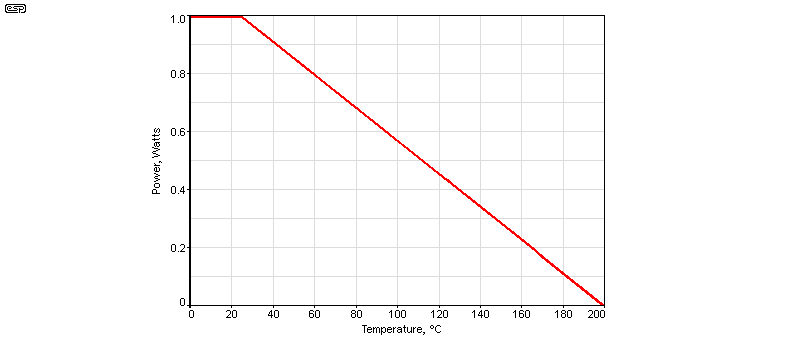
Figure 3 - Zener Diode Temperature Derating
Like all semiconductors, zeners must be derated if their temperature is above 25°C. This is always the case in normal use, and if the guidelines above are used then you usually won't need to be concerned. The above graph shows the typical derating curve for zener diodes, and this must be observed for reliability. Like any other semiconductor, if a zener is too hot to touch, it's hotter than it should be. Reduce the current, or use the boosted zener arrangement described in AN-007.
Zener diodes can be used in series, either to increase power handling or to obtain a voltage not otherwise available. Do not use zeners in parallel, as they will not share the current equally (remember that most are 10% tolerance). The zener with the lower voltage will 'hog' the current, overheat and fail. When used in series, try to keep the individual zener voltages close to the same, as this ensures that the optimum current through each is within the optimum range. For example, using a 27V zener in series with a 5.1V zener would be a bad idea because the optimum current through both cannot be achieved easily.
Using zener diodes as regulators is easy enough, but there are some things that you need to know before you wire everything up. A typical circuit is shown below for reference, and is not intended to be anything in particular - it's simply an example. Note that if you need a dual supply (e.g. ±15V), then the circuit is simply duplicated for the negative supply, reversing the polarity of the zener and C1 as required. We will use a 1W zener, in this case a 1N4744, a 15V diode. The maximum current we'd want to use is about half the calculated maximum (no more than 33mA). The minimum acceptable current is around 10% (close enough to 7mA).
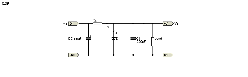
Figure 4 - Typical Zener Regulator Circuit
Firstly, you need to know the following details about your intended circuit ...
When you have this information, you can determine the series resistance needed for the zener and load. The resistor needs to pass enough current to ensure that the zener is within its linear region, but well below the maximum to reduce power dissipation. If the source voltage varies over a wide range, it may not be possible to use a simple zener regulator successfully.
Let's assume that the source voltage comes from a 35V power supply used for a power amplifier. The maximum voltage might be as high as 38V, falling to 30V when the power amp is driven to full power at low mains voltage. Meanwhile, the preamp that needs a regulated supply uses a pair of opamps, and draws 10mA. You want to use a 15V supply for the opamps. This is all the required info, so we can do the calculations. Vs is source voltage, Is is source current, Iz is zener current, IL is load current and Rs is source resistance.
Iz (max) = 30mA (worst case, no load on main supply and maximum mains voltage)
IL = 10mA (current drawn by opamps)
Is (max) = 40mA (again, worst case total current from source)
From this we can work out the resistance Rs. The voltage across Rs is 23V when the source voltage is at its maximum, so Rs needs to be ...
Rs = Vs / I = 23 / 40m = 575 ohms
When the source voltage is at its minimum, there will be only 15V across Rs, so we need to check that there will still be enough zener current ...
Is = V / R = 15 / 575 ohms = 26mA
Iz = Is - IL = 26mA - 10mA = 16mA
When we take away the load current (10mA for the opamps), we still have a zener current of 16mA available, so the regulation will be quite acceptable, and the zener diode won't be stressed. 575 ohms is not a standard value, so we'd use a 560 ohm resistor instead. There's no need to re-calculate everything because the change is small and we were careful to ensure that the design was conservative to start with. The next step is to work out the worst case power dissipated in the source resistor Rs ...
Is = 23V / 560 ohms = 41mA P = Is² × R = 41mA² * 560 ohms = 941mW
In this case, it would be unwise to use less than a 2W resistor, but a 5W wirewound type would be better. In the same way as the resistor power was calculated, it's also a good idea to double check the zener's worst case dissipation. It may be possible to disconnect the opamps, in which case the zener will have to absorb the full 41mA, so dissipation will be 615mW. That's higher than the target set at the beginning of this exercise, but it's within the zener's 1W rating and will never be a long-term issue. Normal worst case dissipation is only 465mW when the opamps are connected, and that's quite acceptable.
Figure 4 shows a 220µF capacitor in parallel with the zener. This does not make any appreciable difference to the output noise, because the impedance (aka dynamic resistance) of the zener is so low. We used an example of a 15V zener, so we expect it's impedance to be about 14 ohms (from the table). To be useful at reducing noise, C1 would need to be at least 1,000uF, but in most cases much lower values are used (typically 100-220uF). The purpose is to supply instantaneous (pulse) current that may be demanded by the circuit, or in the case of opamps, to ensure that the supply impedance remains low up to at least 2MHz or so.
Because zener diodes have a dynamic resistance, there will be some ripple at the output. It's possible to calculate it based on the input ripple, change of source current and the zener's dynamic resistance. Let's assume that there is 2V P-P ripple on the source voltage. That means the current through Rs will vary by 3.57mA ( I = V / R ). The zener has a dynamic resistance of 14 ohms, so the voltage change across the zener must be ...
V = R × I = 14 × 3.57m = 50mV peak-peak (less than 20mV RMS)
Provided the active circuitry has a good power supply rejection ratio (PSRR), 20mV of ripple at 100Hz (or 120Hz) will not be a problem. If that can't be tolerated for some reason, then it's cheaper to use a 3-terminal regulator or a capacitance multiplier than to use any of the established methods for ripple reduction. The most common of these is to use two resistors in place of Rs, and place a high value cap (not less than 470µF) from the junction of the resistors to ground. Doing this will reduce the ripple to well below 1mV, depending on the size of the extra capacitor.
The standard resistor zener feed is subject to wide variations of current and power dissipation as the input voltage varies. A simple feedback circuit can help to maintain a very stable current through the zener, and therefore provide a more stable reference voltage. As discussed earlier, a 6.2V zener diode has a very low thermal coefficient of voltage, and if we can ensure it gets a stable current, this further improves the voltage regulation. Feeding a zener with a current source is standard practice in IC fabrication, and it's easy enough to do in discrete designs as well.
Note that all of the circuits shown (with the exception of Figure 7a) are intended to provide a reference voltage into a high impedance load. If significant output current is needed, the outputs should be buffered with a low-offset opamp. This isn't needed provided the load current is at most 1/10th of the zener current (around 250µA for all except Figure 5a).
The circuits shown below are not power supplies, but they provide a fixed reference voltage for a power supply or other circuitry that may require a stable voltage (e.g. a comparator). The circuits compete well with dedicated precision voltage reference, and they are surprisingly good for many applications (other than Figure 5a, which has the worst performance of them all). In each case, the voltage variation is shown as Δ, which indicates the change over the full input voltage range (10V to 30V).
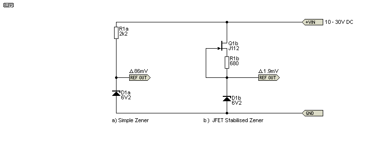
Figure 5 - 'Conventional' Vs. JFET CCS Zener Regulator Circuit
The standard zener regulator (a) will show a typical voltage change of around 85mV from an input voltage of 10-30V, with zener current changing from 1.7mA to over 15mA. This is significantly worse than the stabilised versions (including the JFET), but it may not represent a problem at all if the input voltage is already fairly stable. The JFET current source (b) is a significant improvement. It would be better with a JFET optimised for linear operation, but they are becoming very hard to obtain. I selected the J112 as they are still readily available, but the value of R1b may need to be altered to get a usable zener current (around 2.5mA).
Compare (a) and (b) in the Figure 5 circuits, and it's immediately apparent that the voltage from the JFET stabilised version (b) should be more stable, even with a wide variation of input voltage. Simulated over a voltage range from 10V up to 30V, and a 1.9mV voltage change across the zener in (b), and it follows that zener current and zener power dissipation barely change over the entire voltage range. This also means that ripple rejection is extremely high, so with the addition of a cheap JFET, we can get close to a real precision voltage reference circuit.
In Figure 6, the current mirror (Q2b and Q3b) is fed from a current source (Q1b) which takes its reference from the zener, so there is a closed loop and the current variation through the zener itself can be very small. The circuits shown cannot 'self-start' without R4, because there's no base current available for Q1 until the circuit is operating. R4 provides enough current to start conduction, after which the operation is self-sustaining.
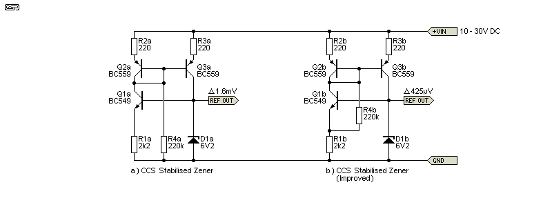
Figure 6 - Precision CCS Zener Regulator Circuits
Using a precision constant current source (CCS) to provide zener current improves performance over a JFET. My original circuit is shown in (a), and a very small change shown in (b) improves matters even more ¹, with the zener variation reduced to 455µV over the input voltage 10-30V range. Note that these were analysed by simulation, but I also built the circuit (results are shown below).
With the values shown, the zener current is only 2.5mA, which seems to defy the guidelines given earlier. However, increasing the zener current doesn't help a great deal, but it increases dissipation in the transistors. For example, if R1 is reduced to 1k, the zener current is increased to 5.4mA, dissipation in Q1 and Q3 is doubled, but the regulation is only improved marginally.
R4 is needed so the circuit can start when voltage is applied, but unfortunately it does adversely affect the performance. A higher resistance reduces the effects, but may cause unreliable start-up. The modification shown in (b) above has better performance than my original and is the recommended connection for optimum performance.
¹ The idea to change the connection of R4 was supplied by a reader who calls himself 'Volt Second'. I extend my thanks, as this improves performance markedly.
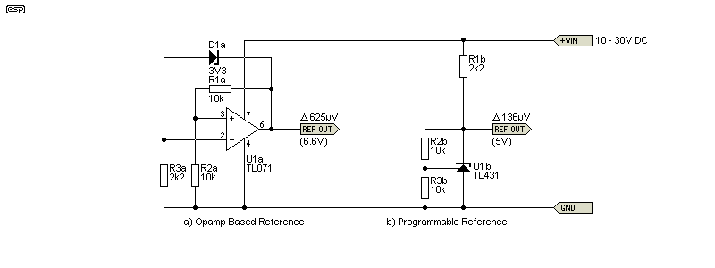
Figure 7 - Opamp Zener Regulator Circuit
The opamp version (a) is a bit of an oddity. The opamp itself has both negative and positive feedback, with the zener diode providing negative feedback once it conducts. The circuit relies on the PSRR of the opamp to minimise voltage variations, and the zener current is a fixed value, based on the zener diode voltage and the resistor to ground (R3). The way the circuit is configured means that the output (reference) voltage is double that of the zener diode, but this can be altered over a small range by varying one or both feedback resistors (R1, R2). Although shown with a TL071, an opamp with better PSRR will improve accuracy. One thing that is not ideal is the zener voltage. Having established that a 6.2V zener is best for thermal stability, that would provide an output voltage of 12.4V. R1a and R2a can only be different by a small amount before the circuit misbehaves. This circuit has one major advantage over the others, in that the opamp can supply output current without it affecting the zener current.
The TL431 programmable voltage reference/ shunt regulator is as good as you might expect. The IC will operate with as little as 1mA cathode current, with a maximum of 100mA, provided the power dissipation limit isn't exceeded. As simulated it's very good, but 'real life' may be different. The temperature variation also has to be considered (typically 4.5mV/°C).
This time around I ran a workbench test on the Figure 6 circuits, and the output voltage changed by only 1.7mV when the input was varied from 10V to 25V (113µV/V). That works out to an input voltage variation attenuation of close to 79dB. I didn't match transistors, and used 5% tolerance resistors in order to get a 'worst-case' result. Considering that a zener diode by itself will vary by at least 86mV over the same voltage range, this is a pretty good result. The supply current changed by only 35µA/V. The measured performance is not as good as the simulation, largely because the simulator has perfectly matched transistors and 0% tolerance resistors. I didn't bother to fiddle with transistors or resistors in the simulations.
In reality, it's unlikely that you will ever need to use any of the more complex stabilised zeners, and they are included here purely in the interests of completeness. Most people will use a TL431 or other adjustable voltage reference (e.g. LM4040, LM329, LM113, etc.) if high performance is needed, but you need to experiment to find the optimum solution for your application.
1 Reverse Biased / Breakdown - Discussing the phenomenon when the diode is reverse biased/breakdown. Bill Wilson
2 RadioElectronics.com - Summary of the zener diode
3 Data Sheet Archive - BZX2C16V Micro Commercial Components 2 Watt Zener Diode 3.6 to 200 Volts.
4 Zener Diode Theory - OnSemi Handbook HBD854/D (No longer available from OnSemi.)
Main Index
App. Notes Index