

|
| Elliott Sound Products | Project 101 |
 Main Index Main Index
 Projects Index Projects Index
|
 Please Note: PCBs are available for this project. Click the image for details.
In various parts of The Audio Pages, I have said that I am not a fan of MOSFET power amplifiers. Well, this amp changed my views, and I consider this to be a 'reference' system in all respects. It uses lateral MOSFETs - not switching types! The latter cannot be used in this circuit - they will self destruct! The performance is extremely good, with vanishingly low distortion levels, plenty of power, very wide full power bandwidth, and the 'self protecting' nature of the lateral MOSFETs themselves.
This is not to suggest that the amp is indestructible (no amplifier can make that claim successfully), but it is much more tolerant of faults than a bipolar transistor amp, and requires nothing more than a pair of zener diodes to limit the current. Having said that, I would still recommend that you avoid shorted output leads and the like - i.e. Don't push your luck. 
One thing that emerged during the design is that PCB layout is absolutely critical. The layout of this new amplifier is similar to that used for the P68 Subwoofer amplifier, and this has some major benefits. P68 has no right to sound as good as it does, and although designed for subwoofer use, it has proven during listening and testing to be a very low distortion design - despite the Class-B output stages. All PCB tracks in the input and driver section are as short as possible, minimising the chance of noise pickup from other sections of the circuit - especially noise/distortion generated by the half-wave signal current handled by each output device.
This MOSFET amplifier is designed to be as flexible as possible, with no bad habits. Indeed, it will operate stably with supply voltages as low as +/-5V (completely pointless, but interesting), all the way to the absolute maximum supply voltage of ±70V. The only change that is needed is to trim the MOSFET bias pot!
With the full supply voltage of ±70V (which must not be exceeded!), continuous ('RMS') power is around 180W into 8 ohms, or 250W into 4ohms. Short term (or 'music') power is typically about 240W into 8 ohms and 380W into 4 ohms. Note that depends to a very great degree on the power supply, and a robust supply is a requirement for the maximum output. The recommended supply voltage is ±56V.
As noted, unless you really need the maximum possible power, I suggest that you use a supply voltage of ±56V obtained from a 40+40V transformer. You will get around 150W into 8 ohms from this supply voltage, but you also relax the demands placed on the MOSFETs and heatsinks. The difference between using ±56V and ±65V is less than 1dB - for the extra peace of mind and relaxed heatsink requirements that's a very small price to pay.
Since this amp probably has more power than you will normally need, even if you do skimp a little on the transformer, the loss will be very small. I must make one thing perfectly clear - this is a hi-fi amplifier. It is not designed for professional PA use, although this is possible if the supply voltage is reduced so that both peak and long term dissipation are maintained regardless of how hard the amp is driven. Although it is quite ok to use with a sub, P68 is a better proposition in that role.
It is worth noting that a MOSFET amp will always produce less power than a bipolar transistor version using the same supply voltage. Even using an auxiliary supply will make only a small difference (one reason I elected not to add the extra complexity). A bipolar design using a ±70V supply can be expected to produce something in the order of 270W into 8 ohms, and well over 500W into 4 ohms. The specified MOSFETs have a rated Vds (saturated voltage, Drain to Source) of 12V at full current, and that is simply subtracted from the DC value of the supply voltage. Using a ±56V supply with a lateral MOSFET amp will always give less power than can be obtained from a bipolar design (see below for measured figures).
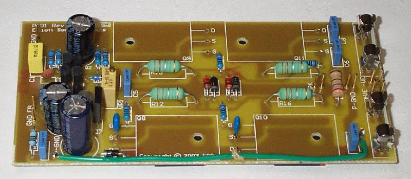
The photo shows the simplicity of the PCB. The MOSFETs are mounted below the board, and are bolted down in the same way as with the P3A and P68 boards. No other mounting is needed. PCB pins or tinned copper wire pins are used as anchor points for the power ground link (the green wire along the front edge), so that the main current carrying tracks were not compromised by running a separate track (which would have required a reduction in size of the positive supply rail).
The entire front-end section is between the electrolytic caps, and is deliberately as compact as possible. This improves performance by ensuring that there are no long tracks for the input stage, which may otherwise pick up noise that can seriously degrade the sound of the amplifier.
The performance of this amp is such that many measurements are very difficult. Some of the more basic measurements are as shown below, based on my custom made transformers which provide ±65V unloaded. Other than output power (which will be ~150W into 8 ohms), the figures are virtually identical with ±56V supplies ...
| Parameter | Measurement | Conditions |
| Output Power | > 180W | < 1% THD, 8Ω |
| > 275W | < 1% THD, 4Ω | |
| DC Offset | < 20mV | Typical |
| Noise | < 2mV RMS | Unweighted (-54dBV) |
| THD | 0.015% | No load, 30V RMS output, 1kHz |
| 0.017% | 8 Ohms, 30V RMS output, 1kHz | |
| 0.02% | 4 Ohms, 30V RMS output, 1kHz | |
| Output Impedance | < 10 mΩ | 1kHz, 4Ω load |
| < 25 mΩ | 10kHz, 4Ω load | |
| Frequency Response | 10Hz to 50kHz | At 1W, -1.5dB |
In particular, the distortion figures show that amp loading causes only very small variations, with any harmonics being predominantly from my audio oscillator. There are no visible or audible high order components to the distortion waveform. Output impedance was measured on a fully built amplifier, including the internal wiring. This entails around 200mm of wire in all (per channel), so the output impedance of the amplifier itself is obviously lower than quoted. For an 8 ohm load, the damping factor at 1kHz is around 800 (8 / 10 milliohms) - completely pointless of course, since any speaker lead will ruin that very quickly.
Noise was measured with inputs open-circuited, and at -54dBV may not look too wonderful, however this figure is very pessimistic. Remember that this is the unweighted measurement, with bandwidth extending to well in excess of 100kHz. Even so, signal to noise ratio (referred to full power) is 86dB unweighted, and the amp is completely silent into typical speakers. Indeed, even connecting a pair of headphones directly to the amp outputs revealed that no noise was audible. Naturally, your methods of construction will differ from mine, and you may not be able to get the same performance.
Intermodulation distortion cannot be measured with the equipment I have available, but I have included a screen capture of the three measurements I took. Most of the harmonic content visible (not that there is a great deal anyway) is present in the two generators I used, and the amplifier contributes virtually nothing.
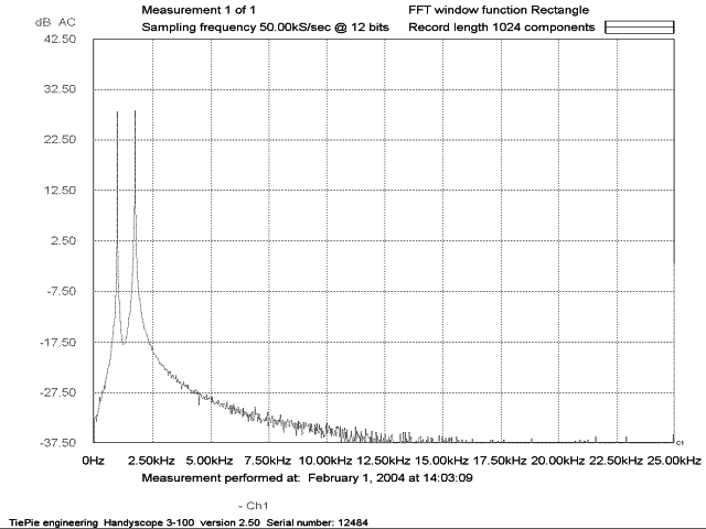
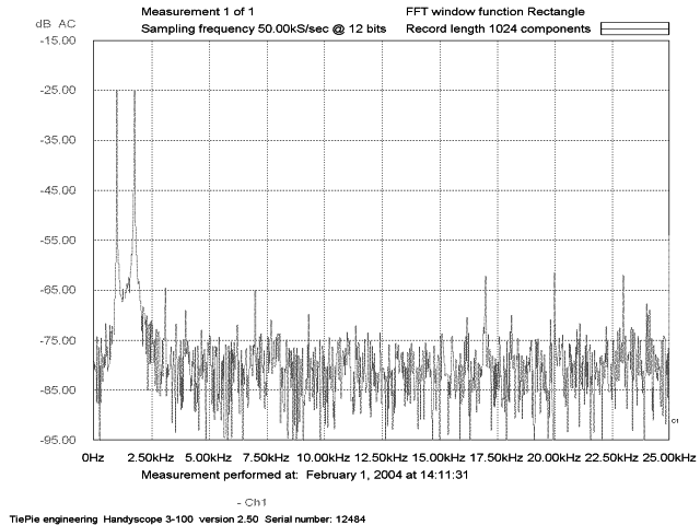
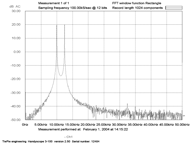
Click on any of the images above for a full resolution version.
The very first thing you will notice is that I have broken with tradition with this amp, and there are no component values shown. Given the performance of the circuit, and the fact that I have already sold a couple as completed, finished amplifiers, I am not about to give away all my secrets for the design. If you want the component values, you must purchase the PCB. There are no exceptions, so don't ask.
The schematic of the amp is shown in Fig. 1, and it is about as simple as a high power MOSFET amplifier can get - it is considerably simpler than most, but lacks nothing in performance. The circuit diagram belies the ability of the amplifier though, so do not be tempted to think that it cannot perform as well as more complex designs - it does, and exceeds the performance of many (if not most) of them. It will be seen that I elected to use a bootstrap current source rather than an active version - there is negligible cost difference, but I was unwilling to make such a radical change after testing the prototype and being so impressed with the results. (If it ain't broke, don't fix it!)
The front end is a conventional long-tailed pair (LTP) using a current mirror load and an active current sink in the 'tail'. Interestingly, adding the current mirror made no difference to distortion, but reduced the DC offset to less than 25mV. The improvement was such that I elected to retain the mirror.
In tests thus far (both measurement and listening), I have been unable to detect even a hint of what is commonly referred to as the 'MOSFET sound'. The relatively high levels of low order distortion and susceptibility to crossover (or 'notch' distortion that plague many MOSFET designs are completely missing - indeed, even with zero bias on the MOSFETs, crossover distortion below 10kHz is barely measurable, let alone audible!
Note Carefully:
The most critical aspect of the design is the PCB layout, and it is very doubtful that if you make your own board, that you will get performance even approaching mine. Power output is essentially unchanged, but distortion and stability are achieved by a compact and carefully designed layout for the front end and driver circuits, which minimises any adverse PCB track coupling that causes much higher distortion levels, and may cause oscillation.
This is not a ploy on my part to get people to purchase my PCBs - that has already been taken care of by leaving out the component values. The simple fact is that unless the PCB layout is done with the utmost care, any amplifier can be made to have far greater distortion levels and reduced stability margins than the published figures suggest.
As shown in the schematics below (figures 1 and 2), the amplifier can be made in high or low power version, and although there is a bit of vacant PCB real estate in the low power design, it is significantly cheaper to make and will be more than sufficient for most constructors. If this version is built (using only 1 pair of MOSFETs), IMO it is essential to limit the supply voltage to ±42V so that it can drive both 4 and 8 ohm loads without excess dissipation. With this voltage, expect about 80W continuous into 8 ohms, and around 140W into 4 ohms. Naturally, dual MOSFET pairs may be used at this voltage as well, providing much better thermal performance (and therefore cooler operation), far greater peak current capability and slightly higher power. This version may be used at any voltage from ±25V to ±42V.
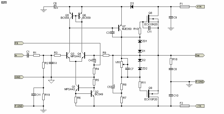
The lateral MOSFETs used were Hitachi/ Renesas lateral devices, 2SK1058 (N-Channel) and 2SJ162 (P-Channel), however these are now obsolete. Lateral MOSFETs are designed specifically for audio, and are far more linear than the (currently) more common switching devices that many MOSFET amps use. Unfortunately, they are not especially cheap, but their performance in an audio circuit is so much better than vertical MOSFETs, HEXFETs, etc., that there is no comparison. Note that using HEXFETs or any other vertical MOSFET type is not an option. They will fail in this circuit, as it was not designed to use them (and their pinout is reversed!).
The alternative is the Exicon ECX10N20 and ECX10P20 (available from Profusion PLC in the UK). These have been used in most of the amps I have built, and they work very well. So potential constructors can verify that the semiconductors are available before purchasing a PCB, this information has now been included. You may also use BUZ901P/BUZ906P or ALF08N16V/ALF08P16V devices. Minimum voltage rating is 160V. All other parts are quite standard. Renesas makes the 2SK2221/2 and 2SJ351/2 lateral MOSFETs as well (not stocked by most suppliers). These are lower power (100W dissipation) but fairly reasonably priced, and should be suitable with reduced power supply voltages. ±42V is the suggested maximum voltage using 2 pairs in the high power config shown next. You might get away with using them at ±56V, but you will be pushing them close to their limits, especially as the heatsink gets warm. ±56V will be alright if your load impedance will not be less than 8 ohms.
The same PCB is used, but has an extra pair of MOSFETs. Since the devices are running in parallel, source resistors are used to force current sharing. Although these may be replaced by wire links, I do not recommend this. This version may be operated at an absolute maximum supply voltage of ±70V (±56V is recommended), and will give up to 180W RMS into 8 ohms, and 250W into 4 ohms. Short term (peak) power is around 240W into 8 ohms and 380W into 4 ohms. These figures are very much dependent on your power supply regulation, determined by the VA rating of the transformer, size of filter caps, etc.
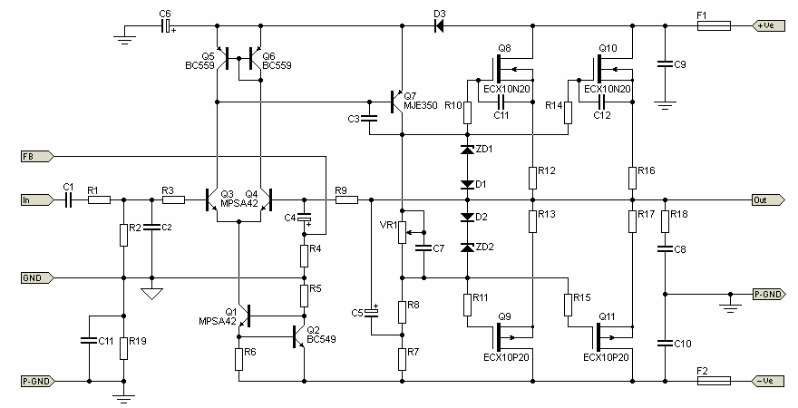
The transistors and MOSFETs are the same in this version as for the low power variant. The additional capacitors (C11 and C12) shown are to balance the gate capacitance. The P-Channel MOSFETs have significantly higher gate capacitance than their N-Channel counterparts, and the caps ensure that the two sides of the amp are roughly equal. Without these caps, the amp will almost always be unstable.
As noted above, the PCB is the same for both versions, but for Fig. 2 it is fully populated with 2 pairs of power MOSFETs. The high power version may also be used at lower supply voltages, with a slight increase in power, but considerably lower operating temperatures even at maximum output, and potentially greater reliability.
With both versions, the constructors' page gives additional information, and the schematics there include an enhanced Zobel network at the output for greater stability even with the most difficult load. This is provided for on the PCB, and allows the amp to remain stable under almost any conditions.
The entire circuit has been optimised for minimum current in the Class-A driver, while still providing sufficient drive to ensure full power capability up to 25kHz. The slew rate is double that required for full power at 20kHz, at 15V/µs, and while it is quite easy to increase it further, this amp already outperforms a great many other amps in this respect, and faster operation is neither required nor desirable.
Note - There are actually two caps marked C5, and two marked C6. This is what is on the PCB overlay, and naturally was not found until it was too late. Since these caps cannot be mixed up, it will not cause a problem.
In both versions of the amp, R7 and R8 are selected to provide 5mA current through the voltage amplifier stage. You will need to change the value to use a different supply voltage ...
R7 = R8 = Vs / 10 (k) (Where Vs is one supply voltage only)
For example, to set the correct current for ±42V supplies ...
R7 = R8 = 42 / 10 = 4.2k (use the next lower standard value - 3.9k)
As suggested above, I strongly recommend that you purchase the PCB for this amplifier, or you will almost certainly get results that are nowhere near the amp's real ability. The PCB also makes construction a breeze, with everything except the power supply mounted on the board itself. Like many other ESP power amps, the MOSFETs are mounted underneath the board, requiring only two (or four) screws to attach the PCB and output devices. As always, full construction details will be available in the ESP secure site when you purchase the board(s).
Heatsinks for an amp like this are always going to be an issue. Since the amp is intended for hi-fi use, fans are undesirable, so the heatsink needs to be substantial. I suggest that you aim for a heatsink with a thermal resistance of around 0.4°C/W for the high power version. It can be somewhat smaller for the low power version of course, but I recommend that it be no smaller than ~1°C/W.
The heatsinks used must have a completely flat back, without any protrusions or anything else that prevents the MOSFETs from making perfect contact with the heatsinks. The MOSFETs must be electrically isolated from the heatsink, and you can use thin mica, Kapton (25um) or aluminium oxide insulators. Do not attempt to use silicone pads - they have far too much thermal resistance and will result in MOSFET failure.
The suggested power supply is completely conventional. Although a small amount of additional power can be obtained by using an auxiliary supply (to boost the rail voltage for the MOSFET drive stage), this is at the expense of greater complexity and more things to go wrong and is not an option here. The transformer for the supply should be matched to the expected power you wish to obtain from the amp.
The following table shows the recommended transformer voltage and VA rating for a single channel only - either use two transformers or a single unit with twice the VA rating shown for stereo. However, in most cases you can use a smaller transformer than that shown without concern for normal home use. Continuous power will be reduced, but with typical audio programme material it's very doubtful that you will hear any difference. For example, a 40-0-40V 300VA transformer can be used for a stereo 150W (8Ω) amp that's used for hi-fi (but not for continuous high power applications). For best performance I suggest a 500VA transformer as that can also handle 4Ω loads.
AC Volts DC Volts VA Power (8Ω) 20-0-20 ±28V 100 40 Probably too low for most applications, but perfectly usable if only low power is needed 25-0-25 ±35V 100 50 Fine for use in a biamped hi-fi system 30-0-30 ±42V 160 80 Maximum voltage for low power version 40-0-40 ±56V 200 150 Recommended supply voltage for high power version. 200VA is the absolute minimum! 50-0-50 ±70V 300 240 Absolute maximum. Can be used, but not recommended - aim for a lower voltage if possible
Note that all powers shown are 'short term' or peak - continuous power will always be less as the supply collapses under load. Peak power levels are usually achieved (or approached) with most music because its transients are generally between 6dB and 10dB greater than the average power output. Transformer VA ratings shown are a guide only - larger or smaller units may be used, with a marginal increase or reduction of peak power. Always use at least the size shown for subwoofer use! Values in bold are preferred, and will give enough power for most systems along with optimum reliability and low operating temperature.
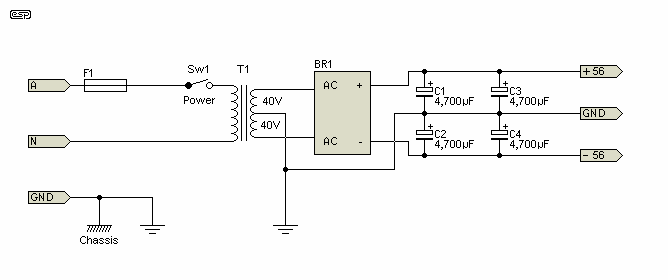
Figure 3 shows the power supply circuit diagram for a ±56V supply, and there is nothing new about it. As I always recommend, the bridge rectifier should be a 400V/35A chassis mount type, and should be properly mounted to a heatsink (or the chassis if aluminium) using heatsink compound.
Filter capacitors must be rated to at least the nominal supply voltage, and preferably higher. If possible, use 105°C rated caps, and join the earthed terminals very solidly to form the star earthing point.
Note - The fuse should be selected according to the size of the power transformer. For any toroidal transformer over 300VA, a soft start circuit is highly recommended. Use the transformer manufacturer's suggested fuse - if this information is not available, ask the supplier - not me!
The DC supply must be taken from the capacitor terminals - never from the bridge rectifier. Using several small capacitors will give better performance than a single large one, and is usually cheaper as well. For example, the performance of 10 x 1,000µF capacitors is a great deal better (in all respects) than a single 10,000µF cap, at between 50% to 70% of the cost of the large unit. This lunch is not free, but it is heavily discounted. 
When you purchase the PCB, you will not only get all component values, but will also have access to information for a power supply that is optimised for the best possible performance for a conventional supply. There is nothing especially innovative about the 'advanced' supply schematic, but the overall results will surprise you.
If your transformer is over 300VA I recommend that you include a Project 39 soft-start circuit. The inrush current of large toroidal transformers is high, and using a soft-start reduces instantaneous stresses on the transformer, bridge rectifier and filter capacitors.
Connect to a suitable power supply - remember that the supply earth (ground) must be connected! When powering up for the first time, use 10 ohm to 22 ohm 'safety' resistors in series with each supply to limit the current if you have made a mistake in the wiring.
For a much more detailed description of the general test processes (as well as troubleshooting information if the amp does not work), please see the Troubleshooting & Repair Guide. That article has much more detailed information than I can include in each project page.
 Main Index Main Index
 Projects Index Projects Index
|