

|
| Elliott Sound Products | Balanced Interfaces |
 Main Index
 Articles Index
Firstly, I'd like to thank Bill Whitlock for giving permission to re-publish this material. There is a great deal of confusion, disinformation and unmitigated nonsense on the Net when it comes to any discussion of balanced systems. The following material unashamedly recommends Jensen transformers and the THAT Corporation's InGenius® IC that was patented by Bill, and provides far better performance in critical applications than any of the standard active balanced receivers.
The remainder of the material (which is copious) covers the principles involved in great detail. It is important to understand that one of the biggest issues with any balanced connection is the so-called 'Pin 1 Problem', where noise is injected into the equipment circuitry from the cable shield. As noted within the article, randomly disconnecting one end or the other of a cable's shield is almost always a bad idea - the problem must be solved within the equipment. Disconnecting the mains safety earth is always a bad idea. It is provided to ensure safety, and is especially important with 230V (50Hz) mains.
While Bill's material was originally dedicated to 120V 60Hz systems, where necessary I have included the relevant information for 230V 50Hz countries. Bear in mind that UL certification has no meaning outside the US and Canada, and local regulations can be quite variable. Many countries (including Australia) now follow the European (IEC) regulations fairly closely, so if in doubt, you must verify that what you intend to do is legal where you live.
As noted within the text, the 600Ω line came from the early telephone systems - as did a vast amount of the technology that we now take for granted. Telephone engineering was at the very forefront of early electronics, and much as we love to hate telephone companies, we owe the early pioneers a great deal for their contributions to audio. While not relevant to this article, it's worth noting that modern 'phone lines are no longer considered to be a nice resistive 600 ohms in most countries. Various 'complex' impedance models are now used instead, because they resemble an actual line more accurately than a simple resistive impedance. Impedance matching (to the 'new' complex impedance) and longitudinal balance are just as important as ever for analogue telephone lines that are extended to millions of households from local exchanges (central offices) throughout the world.
One point needs to be made, and that is the correct wiring for an XLR or stereo phone plug (TRS - tip, ring and sleeve). The proper connections are shown below, and while there have been deviations they are essentially an abomination. The 'Pin 3 Hot' technique was used by some US manufacturers for unbalanced inputs, simply to save time! A single bus was used to bridge pins 1 and 2 along the length of unbalanced inputs, because it was easy (therefore fast and cheap). It was a bad idea then, and it's still a bad idea. Pin 2 is 'Hot' - end of story!

XLR And TRS (Tip, Ring & Sleeve) Connections
I haven't shown the 'TRRS' (tip, ring, ring & sleeve) because it's generally only used for mobile (cell) phones and some tablets and/or other consumer devices. While the sleeve is supposed to be earth/ ground, a certain company (that makes iThings) managed to stuff that up, by deciding that the sleeve would be for the mic connection. A seriously bad idea, but others had to follow suit so headsets and the like would be compatible. Others are also guilty of making changes that were neither necessary nor desirable (some video cameras for example). Unfortunately, when 'marketing' gets a say in design, the result is very often an abomination!
The text below is close to verbatim - metric measurements have been added where necessary. All diagrams have been re-drawn to reflect normal ESP styles and to reduce image size, but are otherwise unchanged. Where additional comments have been made, these are indented, in italics and show a small ESP logo at the end ... like this  .
.
To download a copy of Bill's original PDF from which this material was taken, click here and have a look at the transformer range and other material on the Jensen Transformers website.
Please note: the earth (ground) symbol used in the diagrams below is different from that shown in Bill's original PDF, but it has exactly the same meaning. There is no consensus on the 'correct' symbols for earth/ ground/ chassis, and several different interpretations are to be found with only a cursory search. In all drawings, the earth symbol used indicates the common or 'zero voltage' point of the circuit. This may or may not be connected to protective earth (known as 'earth ground' in the US) and may or may not be connected to the chassis. Bill's original drawings are no different in this respect. I have had one (yes, only one) complaint that the symbols I used are wrong, which I dispute. The 'triangles' used in the original drawings are used to indicate the common, and are also commonly reserved for distinction between analogue and digital earth/ ground points, and often have an 'A' or 'D' within to indicate the difference. However, there are no 'universally' accepted symbols - with the possible exception of the earth symbol shown in the drawings herein, but surrounded by a circle. This means 'protective earth' - i.e. the earth pin on a mains plug or receptacle.
High signal-to-noise ratio is an important goal for most audio systems. However, AC power connections unavoidably create ground voltage differences, magnetic fields, and electric fields. Balanced interfaces, in theory, are totally immune to such interference. For 50 years, virtually all audio equipment used transformers at its balanced inputs and outputs. Their high noise rejection was taken for granted and the reason for it all but forgotten. The transformer's extremely high common-mode impedance - about a thousand times that of its solid-state 'equivalents' - is the reason. Traditional input stages will be discussed and compared. A novel IC that compares favourably to the best transformers will be described. Widespread misunderstanding of the meaning of 'balance' as well as the underlying theory has resulted in all-too-common design mistakes in modern equipment and seriously flawed testing methods. Therefore, noise rejection in today's real-world systems is often inadequate or marginal. Other topics will include tradeoffs in output stage design, effects of non-ideal cables, and the 'pin 1 problem'.
The task of transferring an analog audio signal from one system component to another while avoiding audible contamination is anything but trivial. The dynamic range of a system is the ratio, generally measured in dB, of its maximum undistorted output signal to its residual output noise or noise floor. Fielder has shown that up to 120dB of dynamic range may be required in high-performance sound systems in typical homes [ 1 ]. The trend in professional audio systems is toward increasing dynamic range, fueled largely by increasing resolution in available digital converters. Analogue signals accumulate noise as they flow through system equipment and cables. Once noise is added to a signal, it's essentially impossible to remove it without altering or degrading the original signal.
Therefore, noise and interference must be prevented along the entire signal path. Of course, a predictable amount of random or 'white' noise, sometimes called 'the eternal hiss', is inherent in all electronic devices and must be expected. Excess random noise is generally a gain structure problem, a topic beyond the scope of this paper.
 Ground noise, usually heard as hum , buzz, clicks or pops in audio signals, is generally the most noticeable and irritating - in fact, even if its level is significantly lower than background hiss, it can still be heard by listeners. Ground noise is caused by ground voltage differences between the system components. Most systems consist of at least two devices which operate on utility AC power. Although hum, buzz, clicks, and pops are often blamed on 'improper grounding', in most cases there is actually nothing improper about the system grounding. To assure safety, all user accessible connections and the equipment enclosure must be connected to the safety ground conductor of the AC power system. A properly installed, fully code-compliant AC power distribution system will develop small, entirely safe voltage differences between the safety grounds of all outlets. In general, the lowest voltage differences (generally under 10 millivolts) w ill exist between physically close outlets on the same branch circuit and the highest (up to several volts) will exist between physically distant outlets on different branch circuits. These normally insignificant voltages cause problems only when they exist between vulnerable points in a system - which is more unfortunate than improper. Users who don't understand its purpose will often defeat equipment safety grounding - a practice that is both illegal and extremely dangerous.
Safety must take precedence over all other considerations!
Although UL-approved (or other country specific approval) equipment supplied with a 2-prong power cord is safe, its normal leakage current can also create troublesome ground voltage differences. This topic, as well as unbalanced interfaces, is also beyond the scope of this paper.
Ground noise is very often the most serious problem in an audio system . As Bruce Hofer wrote: "Many engineers and contractors have learned from experience that there are far more audible problems in the real world than failing to achieve 0.001% residual distortion specs or DC-to-light frequency response." [ 2 ]. Carefully designed and executed system grounding schemes can reduce ground voltage differences somewhat but cannot totally eliminate them. The use of 'balanced' line drivers, shielded 'balanced' twisted-pair cables, and 'balanced' line receivers is a long standing practice in professional audio systems. It is tantalising to assume that the use of 'balanced' outputs, cables, and inputs can be relied upon to virtually eliminate such noise contamination. In theory, it is a perfect solution to the ground noise problem, but very important details of reducing the theory to practice are widely misunderstood by most equipment designers. Therefore, the equipment they design may work perfectly on the test bench, but become an annoying headache when connected into a system. Many designers, as well as installers and users, believe grounding and interfacing is a 'black art'. College electrical engineering courses rarely even mention practical issues of grounding.
It's no wonder that myth and misinformation have become epidemic!
The purpose of a balanced audio interface is to efficiently transfer signal voltage from driver to receiver while rejecting ground noise. Used with suitable cables, the interface can also reject interference caused by external electric and magnetic fields acting on the cable. The true nature of balanced interfaces is widely misunderstood. For example "Each conductor is always equal in voltage but opposite in polarity to the other. The circuit that receives this signal in the mixer is called a differential amplifier and this opposing polarity of the conductors is essential for its operation." [ 3 ]. This, like many explanations in print (some in otherwise respectable books), describes signal symmetry - "equal in voltage but opposite in polarity" - but fails to even mention the single most important feature of a balanced interface.
SIGNAL SYMMETRY HAS ABSOLUTELY NOTHING TO DO WITH NOISE REJECTION - IMPEDANCE IS WHAT MATTERS!
A good, accurate definition is "A balanced circuit is a two-conductor circuit in which both conductors and all circuits connected to them have the same impedance with respect to ground and to all other conductors. The purpose of balancing is to make the noise pickup equal in both conductors, in which case it will be a common-mode signal which can be made to cancel out in the load." [ 4 ].
The impedances, with respect to ground, of the two lines is what defines an interface as balanced or unbalanced.
In an unbalanced interface, one line is grounded, making its impedance zero. In a balanced interface, the two lines have equal impedance. It's also important to understand that line impedances are affected by everything connected to them. This includes the line driver, the line or cable itself, and the line receiver. The line receiver uses a differential amplifier to reject common-mode voltages. The IEEE Dictionary defines a differential amplifier as "an amplifier that produces an output only in response to a potential difference between its input terminals (differential-mode signal) and in which output due to common-mode interference voltages on both its input terminals is suppressed" [ 5 ]. Since transformers have intrinsic differential response, any amplifier preceded by an appropriate transformer becomes a differential amplifier.

Figure 1 - Basic Differential Interface Circuit
The basic theory of the balanced interface is straightforward. (For purposes of this discussion, assume that the ground reference of Device A has a noise voltage, which we will call 'ground noise', with respect to the Device B ground reference.) If we look at the HI and LO inputs of Device B with respect to its ground reference, we see audio signals (if present) plus the ground noise. If the voltage dividers consisting of ZO/2 and ZCM on each of the lines have identical ratios , we'll see identical noise voltages at the two inputs of Device B.
Since there is no difference in the two noise voltages, the differential amplifier has no output and the noise is said to be rejected. Since the audio signal from Device A generates a voltage difference between the Device B inputs, it appears at the output of the differential amplifier. Therefore, we can completely reject the ground noise if the voltage divider ratios are perfectly matched. In the real world, we can't perfectly match the voltage dividers to get infinite rejection. But if we want 120 dB of rejection, for example, we must match them to within 0.0001% or 1 part per million!
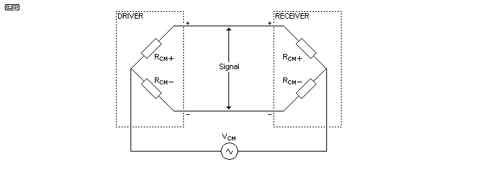
Figure 2 - Equivalent Circuit of Basic Differential Interface Circuit
The ground noise received from Device A, since it exists on or is common to both wires, is called the common-mode voltage and the differential amplifier provides common mode rejection. The ratio of differential or normal-mode (signal) gain to the common-mode (ground noise) gain of the interface is called the common mode rejection ratio or CMRR (called 'longitudinal balance' by telephone engineers) and is usually expressed in dB. There is an excellent treatment of this subject in Morrison's book [ 6 ].
If we re-draw the interface as shown in Figure 2, it takes the familiar form of a Wheatstone bridge. The ground noise is 'excitation' for the bridge and represented as Vcm (common mode voltage). The common mode impedances of the line driver and receiver are represented by RCM+ and RCM-.
When the + and - arms have identical ratios, the bridge is 'nulled' and zero voltage difference exists between the lines - infinite common-mode rejection. If the impedance ratios of the two arms are imperfectly matched, mode conversion occurs. Some of the ground noise now appears across the line as noise.
The bridge is most sensitive to small fractional impedance changes in one of its arms when all arms have the same impedance [ 7 ]. It is least sensitive when upper and lower arms have widely differing impedances. For example, if the lower arms have infinite impedance, no voltage difference can be developed across the line, regardless of the mismatch severity in upper arm impedances. A similar scenario occurs if the upper arms have zero impedance. Therefore, we can minimise CMRR degradation due to normal component tolerances by making common-mode impedances very low at one end of the line and very high at the other [ 8 ]. The output impedances of virtually all real line drivers are determined by series resistors (and often coupling capacitors) that typically have ±5% tolerances. Therefore, typical line drivers can have output impedance imbalances in the vicinity of 10 ohms. The common-mode input impedances of conventional line receivers is in the 10 k to 50 k ohm range, making their CMRR exquisitely sensitive to normal component tolerances in line drivers. For example, the CMRR of the widely used SSM-2141 will degrade some 25 dB with only a 1 ohm imbalance in the line driver.
Line receivers using input transformers (or the InGenius® IC discussed later) are essentially unaffected by imbalances as high as several hundred ohms because their common-mode input impedances are around 50 M ohms - over 1000 times that of conventional 'active' receivers.
Note that this discussion has barely mentioned the audio signal itself. The mechanism that allows noise to enter the signal path works whether an audio signal is present or not. Only balanced impedances of the lines stop it - signal symmetry is irrelevant. When subtracted (in the differential amplifier), asymmetrical signals: +1 minus 0 or 0 minus -1 produce exactly the same output as symmetrical signals: +0.5 minus -0.5. This issue was neatly summarised in the following excerpt from the informative annex of IEC Standard 60268-3:
"Therefore, only the common-mode impedance balance of the driver, line, and receiver play a role in noise or interference rejection. This noise or interference rejection property is independent of the presence of a desired differential signal. Therefore, it can make no difference whether the desired signal exists entirely on one line, as a greater voltage on one line than the other, or as equal voltages on both of them. Symmetry of the desired signal has advantages, but they concern headroom and crosstalk, not noise or interference rejection."
The first widespread users of balanced circuits were the early telephone companies. Their earliest systems had no amplifiers yet needed to deliver maximum audio power from one telephone to another up to 32km (20 miles) away. It's well known that, with a signal source of a given impedance, maximum power will be delivered to a load with the same, or matched, impedance. It is also well known that 'reflections' and 'standing waves' will occur in a transmission line unless both ends are terminated in the line's characteristic impedance. Because signal propagation time through over 30km of line is a significant fraction of a signal cycle at the highest signal frequency, equipment at each end needed to match the line's characteristic impedance to avoid frequency response errors due to reflections. Telegraph companies used a vast network with a huge installed base of open wire pair transmission lines strung along wooden poles. Early telephone companies arranged to use these lines rather than install their own. Typical lines used #6 AWG wire at 12 inch spacing and the characteristic impedance was about 600 ohms, varying by about ±10% for commonly used variations in wire size and spacing [ 9 ]. Therefore 600 ohms became the standard impedance for these balanced duplex (bi-directional) wire pairs and subsequently most telephone equipment in general.
Not only did these lines need to reject ground voltage differences, but the lines also needed to reject electric and magnetic field interference created by AC power lines, which frequently ran parallel to the phone lines for miles. Balanced and impedance matched transmission lines were clearly necessary for acceptable operation of the early telephone system. Later, to make 'long distance' calls possible, it was necessary to separate the duplexed send/receive signals for unidirectional amplification. The passive 'telephone hybrid' was used for the purpose and its proper operation depends critically on matched 600 ohm source and load impedances. Telephone equipment and practices eventually found their way into radio broadcasting and, later, into recording and professional audio - hence, the pervasive 600 ohm impedance specification.

Figure 3 - Impedance Matched Source and Destination Circuits
In professional audio, however, the goal of the signal transmission system is to deliver maximum voltage, not maximum power. To do this, devices need low differential (signal) output impedances and high differential (signal) input impedances. This practice is the subject of a 1978 IEC standard requiring output impedances to be 50 ohms or less and input impedances to be 10 k or more [ 10 ].
Sometimes called 'voltage matching', it minimises the effects of cable capacitances and also allows an output to simultaneously drive multiple inputs with minimal level losses. With rare exceptions, such as telephone equipment interfaces, the use of matched 600 ohm sources and loads in modern audio systems is simply unnecessary and compromises performance.
Where voltage matching techniques are used in (analogue) telecommunications systems, it is referred to as 'bridging'. The high impedance balanced load is bridged across the 'phone line, allowing signal capture only. This technique is not especially common but is used for line monitoring. It is expected that the telephone line is properly terminated at both ends when bridging is used.
Since performance of the differential line receiver is the most important determinant to system CMRR performance and can, in fact, reduce the effects of other degradation mechanisms , we'll discuss it first. There are two basic types of differential amplifiers: active circuits and transformers. Active circuits are made of op-amps and precision resistor networks to perform algebraic subtraction of the two input signals. The transformer is an inherently differential device which provides electrical isolation of input and output signals.
The active differential amplifier , sometimes called an 'actively balanced input' is realisable in several circuit topologies. These circuits are well known and have been analysed and compared in some detail by others [ 11, 12, 13, 14 ].
In our discussion here, we will assume that op-amps, resistors, and resistor ratios are ideal and not a source of error. The following schematics are four popular versions in their most basic form, stripped of AC coupling, RFI filtering, etc. Because the common-mode input impedances, from either input to ground [ 15 ], are all 20 k ohms, these four circuits have identical CMRR performance. Even when perfectly matched, these impedances are the downfall of this approach. To quote Morrison: "many devices may be differential in character but not all are applicable in solving the basic instrumentation problem" [ 16 ].

Figure 4 - Common Actively Balanced Receiver Circuits
The following graph shows the extreme sensitivity of 60 Hz CMRR vs source impedance imbalance for these circuits. These circuits are almost always tested and specified with either perfectly balanced sources or shorted inputs. In real equipment, imbalances commonly range from 0.2 ohm to 20 ohms, resulting in real-world interface CMRR that's far less than that advertised for the line receiver.
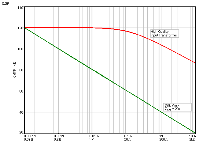
Figure 5 - CMRR vs. Input Source Imbalance in Percent and Ohms
There are other problems:
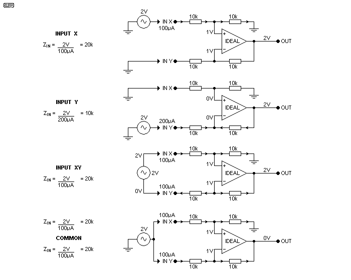
Figure 6 - 'Traditional' Balanced Input Circuit Analysis
An audio transformer couples a signal magnetically while maintaining electrical (aka galvanic) isolation between input and output. It is an inherently differential device, requiring no trimming and its differential properties are stable for life. The next graph shows a circuit simulation model for a Jensen JT-10KB-D line input transformer.
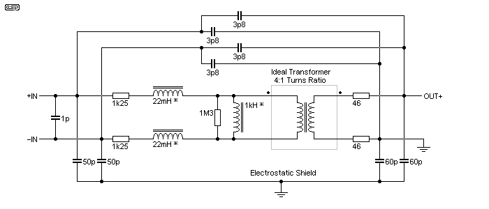
Resistance in Ohms, capacitors in Farads, and inductance in Henrys. |
Its common-mode input impedances are determined by the 50 pF capacitances of the primary to the Faraday shield, which is grounded, and small parasitic capacitances to the secondary, one end of which is usually grounded. These high common-mode input impedances, about 50 M ohms at 60 Hz and 1 M ohms at 3 kHz, are responsible its relative insensitivity to large source impedance imbalances, as shown in the previous graph. There are other advantages, too:
Noise rejection in a real-world balanced interface is often far less than that touted for th e receiving input. That's because the performance of balanced inputs have traditionally been measured in ways that ignore the effects of line driver and cable impedance imbalances. For example, the old IEC method essentially 'tweaked' the driving source impedance until it had zero imbalance. Another method, which simply ties the two inputs together and is still used by many engineers, is equally unrealistic and its results essentially meaningless. This author is pleased to have convinced the IEC, with the help of John Woodgate, to adopt a new CMRR test that inserts realistic impedance imbalances in the driving source. The new test is part of the third edition of IEC Standard 60268-3, Sound System Equipment - Part 3: Amplifiers, issued in August 2000. A schematic of the old and new test methods is shown below. It's very important to understand that noise rejection in a balanced interface isn't just a function of the receiver - actual performance in a real system depends on how the driver, cable, and receiver interact.
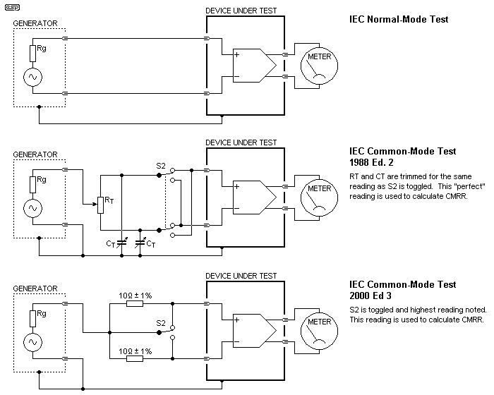
Figure 8 - IEC Normal-Mode and Common-Mode Test Circuits
The new circuit uses a technique known as 'bootstrapping' to raise the AC common-mode input impedance of the receiver to over 10 M ohms at audio frequencies. The schematic below shows the basic technique. By driving the lower end of R2 to nearly same AC voltage as the upper end, current flow through R2 is greatly reduced, effectively increasing its value. At DC, of course, Z is simply R1 + R2. If gain G is unity, for frequencies within the passband of the high-pass filter formed by C and R1, the effective value of R2 is increased and will approach infinity at sufficiently high frequencies. For example, if R1 and R2 are 10k each, the input impedance at DC is 20 k. This resistance provides a DC path for amplifier bias current as well as leakage current that might flow from a signal source. At higher frequencies, the bootstrap greatly increases the input impedance, limited ultimately by the gain and bandwidth of amplifier G. Impedances greater than 10 M ohms across the audio spectrum can be achieved. Another widely used balanced input circuit is called an instrumentation amplifier. The circuit shown below is a standard instrumentation amplifier modified to have its input bias resistors , R1 and R2, bootstrapped. Note that its common-mode gain, from inputs to outputs of A1 and A2, is unity regardless of any differential gain that may be set by RF and RG. The common-mode voltage appearing at the junction of R3 and R4 is buffered by unity gain buffer A4 which, through capacitor C, AC bootstraps input resistors R1 and R2. To AC common-mode voltages, the circuit's input impedances are 1000 or more times the values of R1 and R2, but to differential signals, R1 and R2 have their normal values, making the signal input impedance R1 + R2. Note that capacitor C is not part of the differential signal path, so signal response extends to DC. The bootstrapping does not become part of the (differential) signal path.
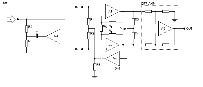
Figure 9 - Input Bootstrap Circuit Raises Impedance
The new circuit also has advantages in suppressing RF interference. Audio transformers inherently contain passive low-pass filters, removing most RF energy before it reaches the first amplifier. In well-designed equipment, RF suppressing low-pass filters must precede the active input stages. A widely-used circuit is shown below. At 10 kHz, these capacitors alone will lower common-mode input impedances to about 16 k ohms. This seriously degrades high frequency CMRR with real-world sources, even if the capacitors are perfectly matched. A tradeoff exists because shunt capacitors must have values large enough to make an effective low-pass filter, but small enough to keep the common-mode input impedances high. The new circuit eases this tradeoff.

Figure 10 - Input Low-Pass Filter for RF Suppression
The circuit above also shows how bootstrapping can make the effective value of these capacitors small within the audio band yet become their full value at RF frequencies . By forcing the lower end of C2 to the same AC voltage as the upper, current flow through C2 is greatly reduced, effectively decreasing its value. If gain G is unity, at frequencies below the cutoff frequency of the low-pass filter formed by R and C1, the effective value of C2 will approach zero. At very high frequencies, of course, the effective capacitance is simply that of C1 and C2 in series (C1 is generally much larger than C2). For example, if R = 2 k ohms, C1 = 1 nF, C2 = 100 pF, and G = 0.99, the effective capacitance is only 15 pF at 10 kHz, but increases to 91 pF at 100 kHz or higher. The schematic below shows a complete input stage with bootstrapping of input resistors R1/ R2 and RF filter capacitors C1/ C2. Series filter elements X1 and X2 can be resistors or inductors, which provide additional RFI suppression. A paper by Whitlock describes these circuits in much greater detail [ 8 ].
The InGenius® circuit, covered by US Patent 5,568,561, is licensed to THAT Corporation. The silicon implementation differs from the discrete solution in many respects. Since all critical components are integrated, a well controlled interaction between resistor values and metal traces can be duplicated with similar performance from die to die. But the integration of certain components creates new challenges.
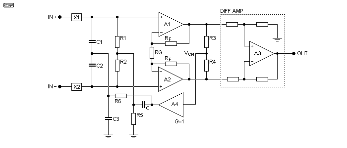
Figure 11 - InGenius® Differential Amplifier
The process used by THAT Corporation for this device is 40-volt Complementary Bipolar Dielectric Isolation (DI) with Thin Film (TF). The DI process has remarkable advantages. Truly high performance PNP and NPN transistors, as good as their discrete counterparts, can be made on the same piece of silicon. Each device is placed in a tub that's isolated from the substrate by a thick layer of oxide. This, unlike more conventional Junction Isolated (JI) processes, makes it possible to achieve hundreds of volts of isolation between individual transistors and the substrate. The lack of substrate connection has several advantages. It minimises stray capacitance to the substrate (usually connected to the negative rail), therefore wider bandwidths can be achieved with a simpler, fully complementary circuit design. Also, it makes possible stable operational amplifier designs with high slew rates. In fact, the typical slew rate of the InGenius® line receiver is better than 10 V/µs.
The op-amp design topology used is a folded cascode with PNP front end, chosen for better noise performance. The folded cascode achieves high gain in one stage and requires only a simple stability compensation network. Moreover, the input voltage range of a cascode structure is greater than most other front ends. The output driver has a novel output stage that is the subject of U S patent 6,160,451. The new topology achieves the same drive current and overall performance as a more traditional output stage but uses less silicon area.
The InGenius® design requires very high performance resistors. Most of the available diffused resistors in a traditional silicon process have relatively high distortion and poor matching. The solution is to use thin film (TF) resistors. The family of thin film resistors include compounds such as, Nichrome (NiCr), Tantalum Nitride (TaNi) and Sichrome (SiCr). Each compound is suitable for a certain range of resistor values. In InGenius, SiCr thin film is used due to its stability over time and temperature and sheet resistance that minimises the total die area. Thin-film on-chip resistors offer amazing accuracy and matching via laser trimming, but are more fragile than regular resistors, especially when subjected to Electrostatic Discharge (ESD). Careful layout design was required to ensure that the resistors can withstand the stress of ESD events.
The CMRR and gain accuracy performance depend critically on matching of resistors. The integrated environment makes it possible to achieve matching that would be practically impossible in a discrete implementation. Typical resistor matching, achieved by laser trimming, in the InGenius® IC is 0.005%, which delivers about 90 dB of CMRR. In absolute numbers, this means the typical resistor and metal error across all resistors is no greater than 0.35 ohms! Discrete implementations with such performance are very difficult to achieve and would be extremely expensive.
Real-world environments for input and output stages require ESD protection. Putting it on the chip, especially for an IC that can accept input voltages higher than the supply rails, posed interesting challenges. The conventional solution is to connect reverse-biased protection diodes from all pins to the power pins. In the InGenius® IC, this works for all pins except the input pins because they can swing to voltages higher than the power supply rails. For the input pins, THAT's designers developed a lateral protection diode with a breakdown voltage of about 70 volts that could be fabricated using the same diffusion and implant sequences used for the rest of the IC.
There are three basic types of line drivers: ground referenced, active floating, and transformer floating. Schematics in Figure 12 show simplified schematics of each type connected to an ideal line receiver having a common-mode input impedance of exactly 20 k ohms per input. (Differential or signal voltage generators are shown in each diagram for clarity, but for common-mode noise analysis the generators are considered short circuits. The receiver ground is considered the zero signal reference and the driver ground is at common-mode voltage with respect to the receiver ground.)
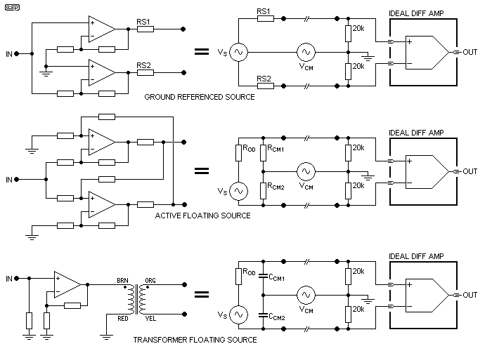
Figure 12 - Balanced Line Driver Topologies
The following graph in Figure 13 compares simulated CMRR performance of the three sources with this receiver setup. The ground referenced source has two anti-phase voltage sources, each referenced to driver ground. The resistive common-mode output impedances are Rs1 and Rs2. The differential output impedance ROD is simply RS1 + Rs2. The common-mode voltage VCM is fed into both line branches through RS1 and RS2. VCM appears at the line receiver attenuated by two voltage dividers formed by RS1 and 20 k ohms in one branch and RS2 and 20 k ohms in the other.
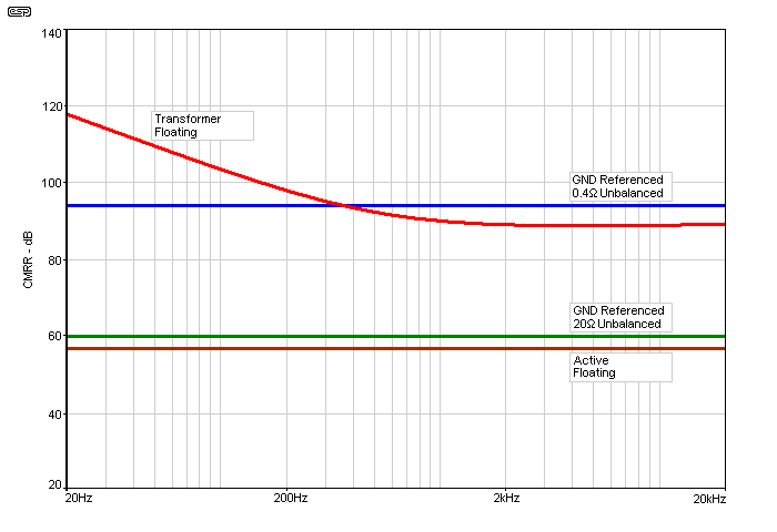
Figure 13 - Balanced Line Driver Performance
As discussed previously, ratio matching errors in these two voltage dividers will degrade CMRR. (It could be argued that Rs1 need not equal Rs2 and that the common-mode input impedances need not match because this condition is not necessary for ratio matching. However, equality is necessary if we wish to allow interchange of system devices.)
Since typical values for RS1 and RS2 are 20 ohms to 100 ohms each with independent tolerances of ±1% to ±10%, worst case source impedance imbalance could range from 0.4 ohms to 20 ohms. With these imbalances, system CMRR will degrade to 94 dB for 0.4 ohms, or to 60 dB for 20 ohms. Since the imbalances are resistive, CMRR is constant over the audio frequency range. The active floating source is built around a basic circuit consisting of two opamps cross-coupled with both negative and positive feedback to emulate a floating voltage source. The resistive common-mode output impedances are RCM1 and RCM2. The differential output impedance is ROD. The common-mode voltage VCM is fed into both line branches through RCM1 and RCM2. VCM appears at the line receiver attenuated by two voltage dividers formed by RCM1 and 20 k ohms in one branch and RCM2 and 20 k ohms in the other, with ROD across the line. ROD is typically 50 to 100 ohms. Since the common-mode output impedances of this circuit are increased by precise balancing of resistor ratios which also interact with output signal balance (symmetry), adjustment is difficult and values for RCM1 and RCM2 are not specified directly. One manufacturer of this circuit specifies output common mode rejection (OCMR) by the BBC test method [ 21 ]. The results of this test can be used to determine the effective values of RCM1 and RCM2 using computer-aided circuit analysis. Values of 5.3 k ohms and 58.5 k ohms were found for a simulated part having OCMR and SBR (signal balance ratio) performance slightly better than the 'typical' specification. For this simulated part, system CMRR was degraded to 57 dB. Since the imbalances are resistive, CMRR is constant over the audio frequency range.
The transformer floating source consists of a transformer whose primary is driven by an amplifier whose output impedance is effectively zero by virtue of conventional negative feedback. The common-mode output impedances Ccm1 and Ccm2 consist of the interwinding capacitance for multi-filar wound types, or the secondary to shield capacitance for Faraday shielded types. Differential output impedance ROD is the sum of secondary and reflected primary winding resistances. For typical bi-filar transformers, CCM1 and CCM2 range from 7 nF to 20 nF each, matching to within 2%. Typical ROD range is 35 to 100 ohms. System CMRR will be 110 dB to 120 dB at 20 Hz, decreasing at 6 dB per octave since the unbalances are capacitive, to 85 dB to 95 dB at 500 Hz, above which it becomes frequency independent. If, instead of the active receiver, a Jensen JT-10KB-D input transformer is used, its full CMRR capability of about 125 dB at 60 Hz and 85 dB at 3 kHz is realised with any of the sources and conditions described above.
The GROUNDED LOAD behavior of these three sources is an important consideration if unbalanced inputs are to be driven. Of course, for any line driver, either output should be capable of withstanding an accidental short to ground or to the other line indefinitely without damage or component failure. This is best accomplished with current limiting and thermal shutdown features.
The GROUND REFERENCED source will output abnormally high currents into a grounded line. Hopefully, it will current limit, overheat, and shut down. If not, at the system level, it will be forcing high, and probably distorted, currents to a remote ground. These currents, as they return to the driver, will circulate through the grounding network and become common-mode voltages to other devices in the system. The usual symptom is described as 'crosstalk'.
The ACTIVE FLOATING source compromises CMRR, output magnitude balance, and high frequency stability in quest of a 'transformer-like' ability to drive a grounded or 'single-ended' input. However, to remain stable, the grounded output must be carefully grounded at the driver [ 22, 23 ]. Since this makes the system completely unbalanced, it is a serious disadvantage.
The TRANSFORMER FLOATING source breaks the ground connection between the driver and the unbalanced input. Because the transformer secondary is able to 'reference' its output to the unbalanced input ground, power line hum is reduced by more than 70 dB in the typical situation shown in the schematic in Figure 14. Because the ground noise is capacitively coupled through Ccm1, reduction decreases linearly with frequency to about 40 dB at 3 kHz.
With the transformer floating source, if it is known that an output line will be grounded, an appropriate step can be taken to optimise performance. With a differentially driven transformer, drive should be removed from the corresponding end of the primary to reduce signal current in the remotely grounded output line. In the case of single-ended driven transformer, simply choose the secondary line corresponding to the grounded end of the primary for grounding.

Figure 14 - Transformer Output Driving Unbalanced Input
Grounding one output line at the driver, which is required to guarantee stability of most 'active floating' circuits, degenerates the interface to a completely unbalanced one having no ground noise rejection at all.
The primary effects on system behavior caused by the interconnecting shielded twisted pair (often called STP) cable is caused by the capacitance of its inner conductors to the shield. The two inner conductors of widely used 22 gauge foil shielded twisted pair cable, when driven 'common-mode', exhibit a capacitance to the shield of about 220pF per metre (67 pF per foot). But the capacitance unbalance can be considerable. Measurements on samples of two popular brands of this cable showed capacitance unbalances of 3.83% and 3.89%, with the black wire having the highest capacitance in both cases. On one sample, insulation thickness was calculated from outside diameter measurements and assumed that the stranded conductors in both wires conductors were identical. The black insulation was 2.1% thinner and, since capacitance varies as the inverse square of the thickness, this would seem to explain the unbalance.
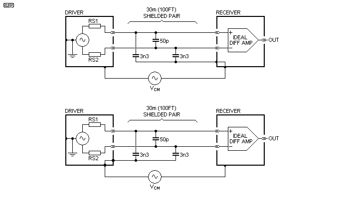
Figure 15 - Effects Of Cable Shield Terminations
Perhaps this topic needs some attention from cable manufacturers. This is important because, if the cable shield is grounded at the receive end, these capacitances and the output impedances of the driver form two low-pass filters. Unless these two filters match exactly, requiring an exact match of both driver output impedances and cable capacitances, mode conversion will take place. Such conversion is aggravated by long cables and unbalanced driver impedances. Because of its high common-mode output impedances, the active floating driver is very vulnerable to this conversion mechanism. Its cable shields must be grounded only at the driver end.
But this conversion CAN be avoided. The upper schematic shows how the common-mode noise is low-pass filtered. Remember that our reference point is the receiver 'ground'. If we simply ground the cable shield at the driver end instead, as shown in the lower schematic, no common-mode voltage appears across the cable capacitances and no filters are formed! Since the shield now is at the common-mode voltage and so are both driver outputs, there is no common-mode voltage across the cable capacitances and they effectively 'disappear'. As far as the common-mode voltage on the signal conductors is concerned, the cable capacitances are now in parallel with the source impedances, virtually eliminating the unbalancing effects of the capacitances.
Grounding of shields at both driver and receiver creates an interesting tradeoff. The cable effects will, predictably, fall between the two schemes described above. The 'advantage' is that, because it connects the two chassis, it can reduce the common-mode voltage itself even though it may degrade the receiver's rejection of it, especially as we approach 20 kHz. It would be far better, of course, to use some other means, such as a dedicated grounding system or even the utility safety ground (power cord 3rd prong), to restrain common-mode voltage. Devices with no safety ground (two prong power cords) are the most offensive in this regard, with their chassis voltage often well over 50 volts AC with respect to system safety ground. The current available is very small, posing no safety hazard, but it creates a very large common-mode voltage unless somehow restrained. As we mentioned earlier, it is NOT necessary to have symmetrical signals on the balanced line in order to reject common-mode noise.
Signal symmetry is a practical consideration to cancel capacitively coupled signal currents which would otherwise flow in the cable shield. In a real system, there will be some signal currents flowing in the shield because of either signal asymmetry or capacitance imbalance in the cable. If the cable shield is grounded only at the driver, these currents will harmlessly flow back to the driver and have no system-level effects. But if the shield is grounded only at the receiver, these currents will return to the driver only after circulating through remote portions of the grounding system. Because the currents rise with frequency, they can cause very strange symptoms or even ultrasonic oscillations at the system level.
Sometimes, especially with very long cables, leaving the shield 'floating' at the receive end may result in increased RF common-mode voltage at the receiver because of antenna effects and high RF fields. To minimise this potential problem, a 'hybrid' scheme can be used to effectively ground the receive-end shield only for RF [ 24 ].
There is yet another reason not to solidly ground the shield at the receive end of the cable. When interference currents flow in their shield, certain cables induce normal-mode noise in the balanced pair. Details on this subject are covered in AES papers by Neil Muncy and Brown-Whitlock. Both conclude that cables utilising a drain wire with the shield are far worse than those using a braided shield without drain wire [ 25, 26 ].
The 'Pin 1 Problem'
Dubbed the 'pin 1 problem' (pin 1 is shield in XLR connectors) by Neil Muncy, common-impedance coupling has been inadvertently designed into a surprising number of products with balanced interfaces. As Neil says, "Balancing is thus acquiring a tarnished reputation, which it does not deserve. This is indeed a curious situation. Balanced line-level interconnections are supposed to ensure noise-free system performance, but often they do not" [ 26 ].

Figure 16 - Pin 1 Problem Allows Shield Currents to Flow in Signal Circuitry
The pin 1 problem effectively turns the SHIELD connection into a very low-impedance SIGNAL input! As shown in Figure 16, shield current, consisting mainly of power-line noise, is allowed to flow in internal wiring or circuit board traces shared by amplifier circuitry. The tiny voltage drops created are amplified and appear at the device output. When this problem exists in systems, it can interact with other noise coupling mechanisms to make noise problems seem nonsensical and unpredictable. The problem afflicts equipment with unbalanced interfaces, too. Fortunately, there is a simple test to reveal the pin 1 problem. The 'hummer' is an idea suggested by John Windt [ 27 ]. This simple device, which might consist of only a 'wall-wart' transformer and a resistor, forces an AC current of about 50 mA through suspect shield connections in the device under test. In properly designed equipment, this causes no additional noise at the equipment output.
The following steps will ensure that your equipment doesn't create noise problems in real-world systems ...
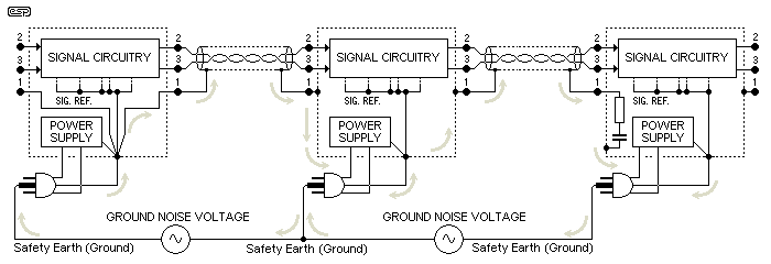
Figure 17 - Avoid Pin 1 Problem with Separate Pathways for Shield Currents
This work is based in part on a 1994 AES paper by this author [ 28 ].
There is a lot of info on the Net about shielding and the so-called 'Pin 1' problem. In particular, Rane has produced some technical notes that will be useful (see [ 29 ] and [ 30 ]), but manufacturers and home builders don't always get it right. In some cases you may find that RF (radio frequency) energy manages to get through despite your very best efforts. Mobile (cell) phones are (or were, depending on the technology used) a potentially useful source of RF for testing, and most people in the industry will be acquainted with the noise made by mobiles. VHF analogue TV transmitters were the bane of many recording studios and live performances, but digital broadcasting seems to have minimised that source of interference. However, many areas will still have analogue TV, so grounding is still a very important part of the set-up.
If the information in this article seems to be more complex than you expected, that's because few explanations have ever gone into the level of detail that's needed to understand balanced interfaces properly. Many people have considered balanced lines to be a panacea, but unless the equipment is designed properly there are many opportunities to mess up the entire process. Properly set up balanced interfaces can ensure trouble-free signal transfer for long distances in very (electrically) noisy environments, but if the proper precautions aren't taken the end result can be just as bad as using completely unbalanced interconnections.
As Bill has pointed out very clearly, the expectation that a balanced connection will have equal but opposite signals on each line is not required. Many very expensive microphones use a scheme where only one signal line is driven. Provided the impedances are matched as described, this method works perfectly. I have previously described this method of obtaining a balanced connection as "Hey, that's cheating" - be that as it may, it works just as well as the 'real thing'. The only down side is that only half the level is available.
For many applications, the use of balanced interconnects is simply not needed at all. In general, a home hi-fi needs balanced interconnects like a fish needs a bicycle, but someone, somewhere, decided that balanced connections 'sound better', but not because of noise reduction. Balanced connections are not used because they sound better or even different from any other. They are used where mains earth (ground) noise causes (or may cause) interference to the signal.
There is also an all pervading myth that only a balanced connection can be truly noise-free when run for long distances. Many very expensive and highly specified sound measurement microphones use a simple coaxial cable and a BNC connector, with a special 'current loop' power supply. The cables can be run for 50 metres or more in virtually any environment without any concern for noise (or hum) pickup. This is equipment at the forefront of both technology and cost, and an unbalanced connection is not used to save a few dollars ... quite the reverse.
Where balanced connections are used (from different pieces of powered equipment), one useful trick is to connect pin 1 of the input XLR connector to chassis via a parallel resistor and capacitor. The resistor prevents high current loops but maintains the electrical connection, and the capacitor shorts any RF noise to chassis. Typical values are 10 ohms in parallel with 100nF. For equipment that will be used for live work (concerts etc.), the resistor should be rated for at least 5W, because a simple connection error during setup can easily burn out lesser resistors. It's not unknown for even metal-clad 20W resistors used in this way to fail (sometimes catastrophically) given a worst case connection mistake. The use of XLR connectors used to be quite common for speaker connections (a very poor choice, but phone/ jack plugs and sockets are much worse!), and a speaker lead plugged into an amplifier input can cause some serious damage.
I urge the reader to re-read this article as many times as necessary to ensure that everything is thoroughly understood. Despite having been with us for a very long time, the 'simple' balanced interface is still the source of more myth and misinformation than any other. A good understanding of the principles, methods and most importantly the reasons for using balanced interfaces will help dispel many long-held but often false beliefs.
Finally, when in doubt or for a 'mission critical' application - USE A TRANSFORMER. The transformer's most attractive and endearing characteristics are that it provides true galvanic isolation (no electrical connection between source and destination electronics) and it has an inherently fully differential output and/or input. If available, winding centre taps should not be connected to ground or to anything else. The exception is when the centre tap is used for phantom power ... which must be connected to the P48V supply via a resistor. Never direct connect the centre tap to the P48 supply voltage. While not exactly standard, a 3.3k resistor may be used without any problems. 
 Main Index
 Articles Index